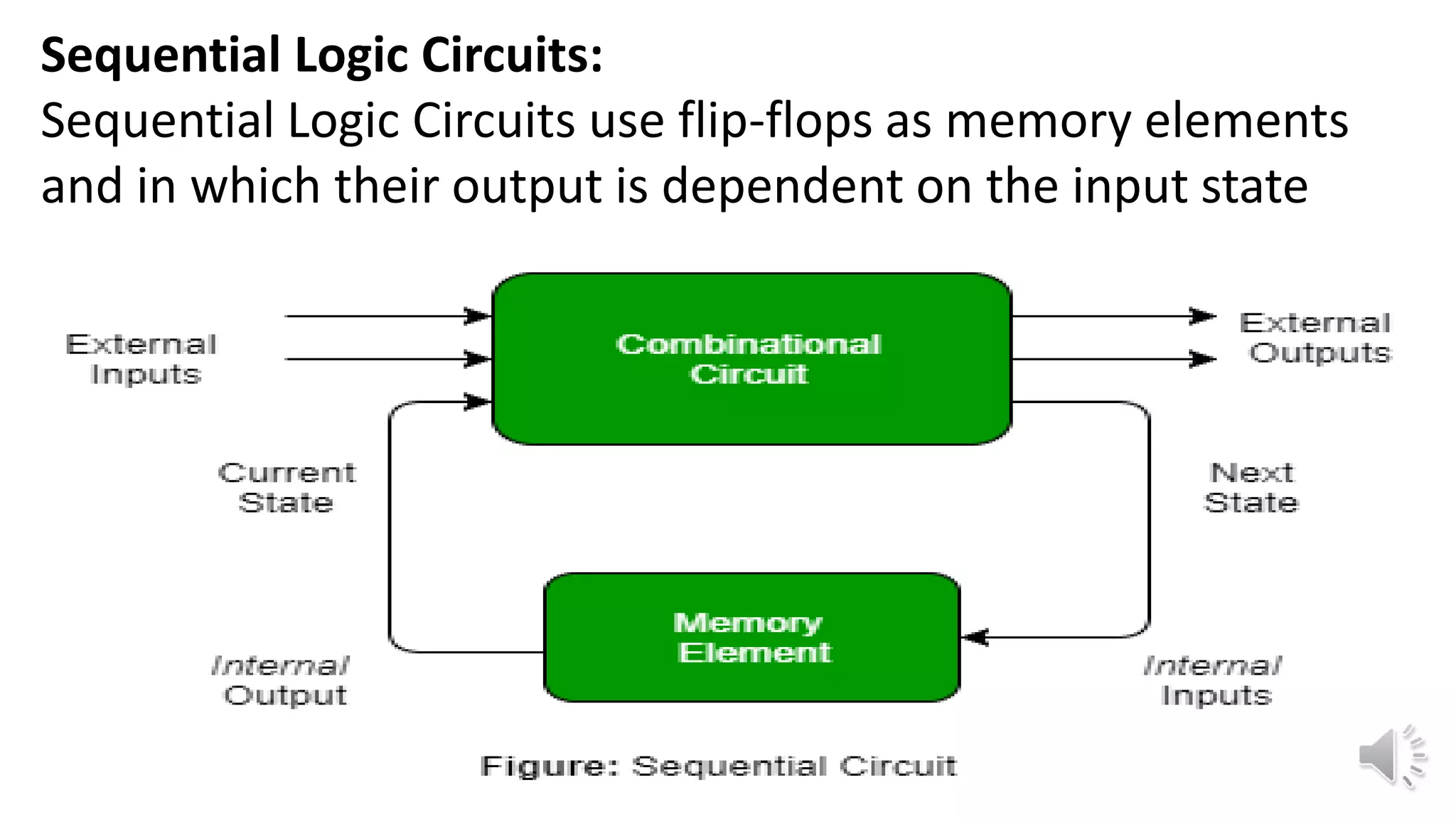
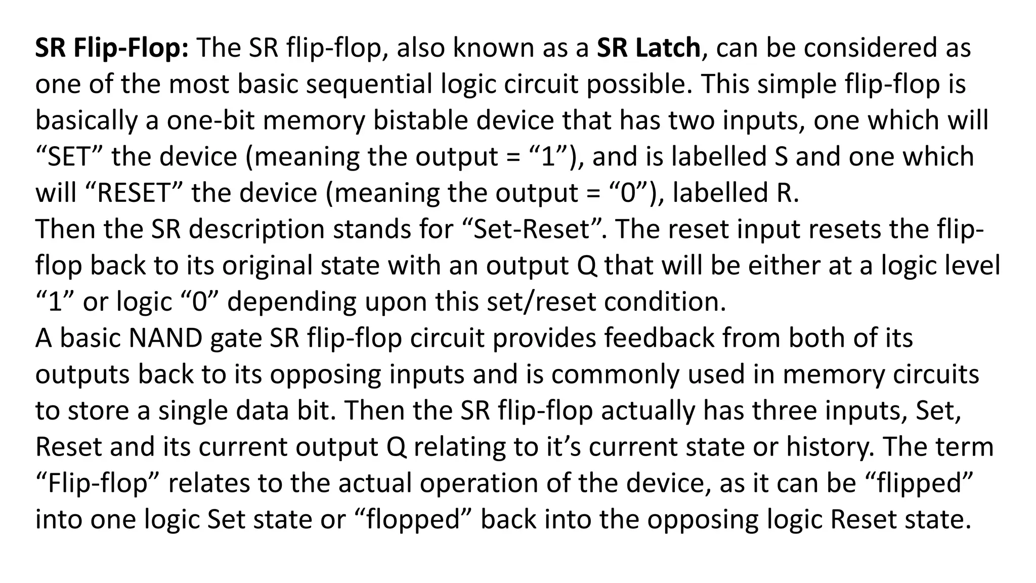
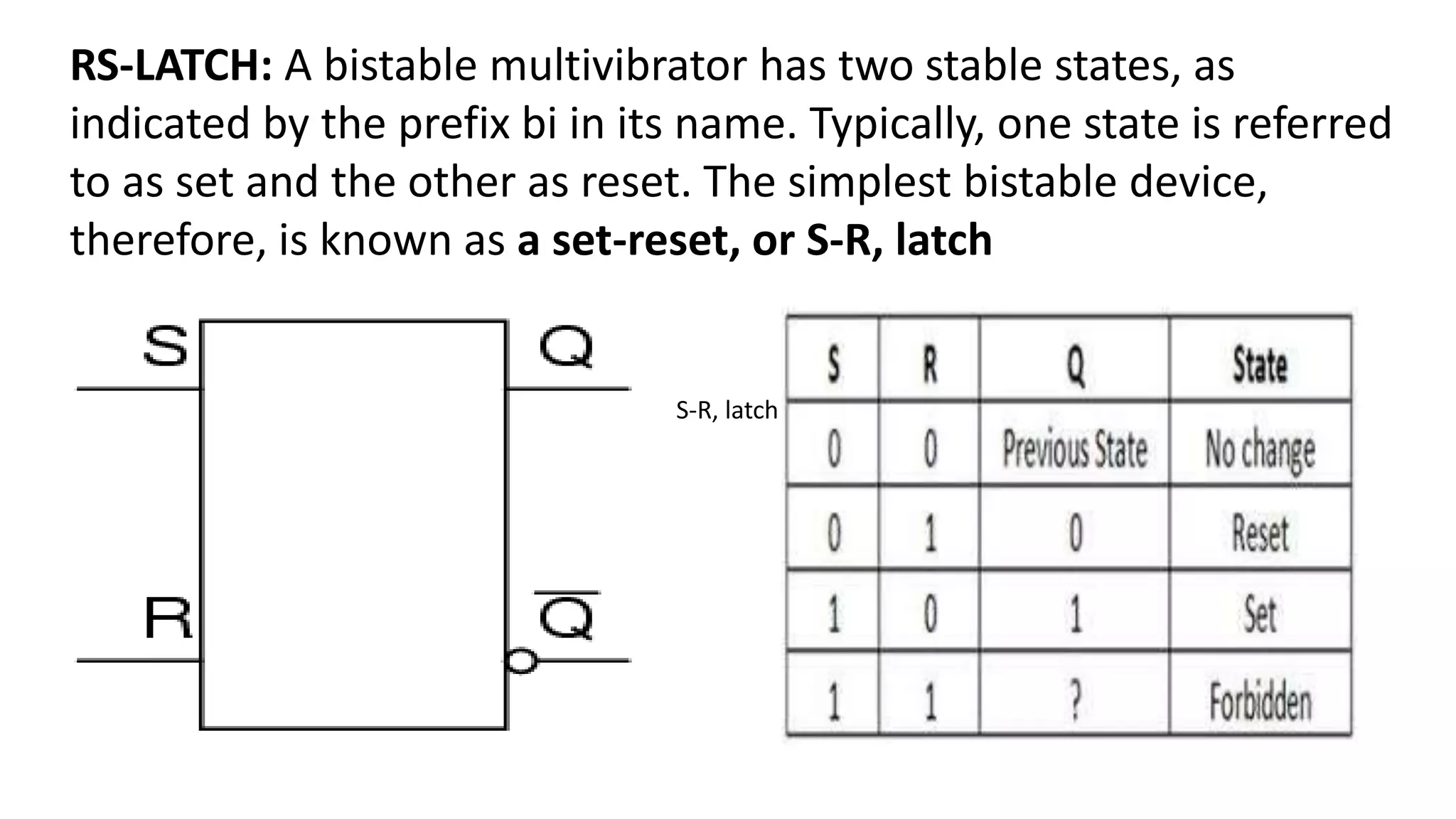
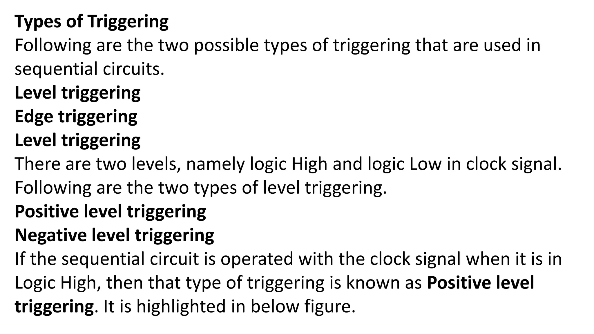
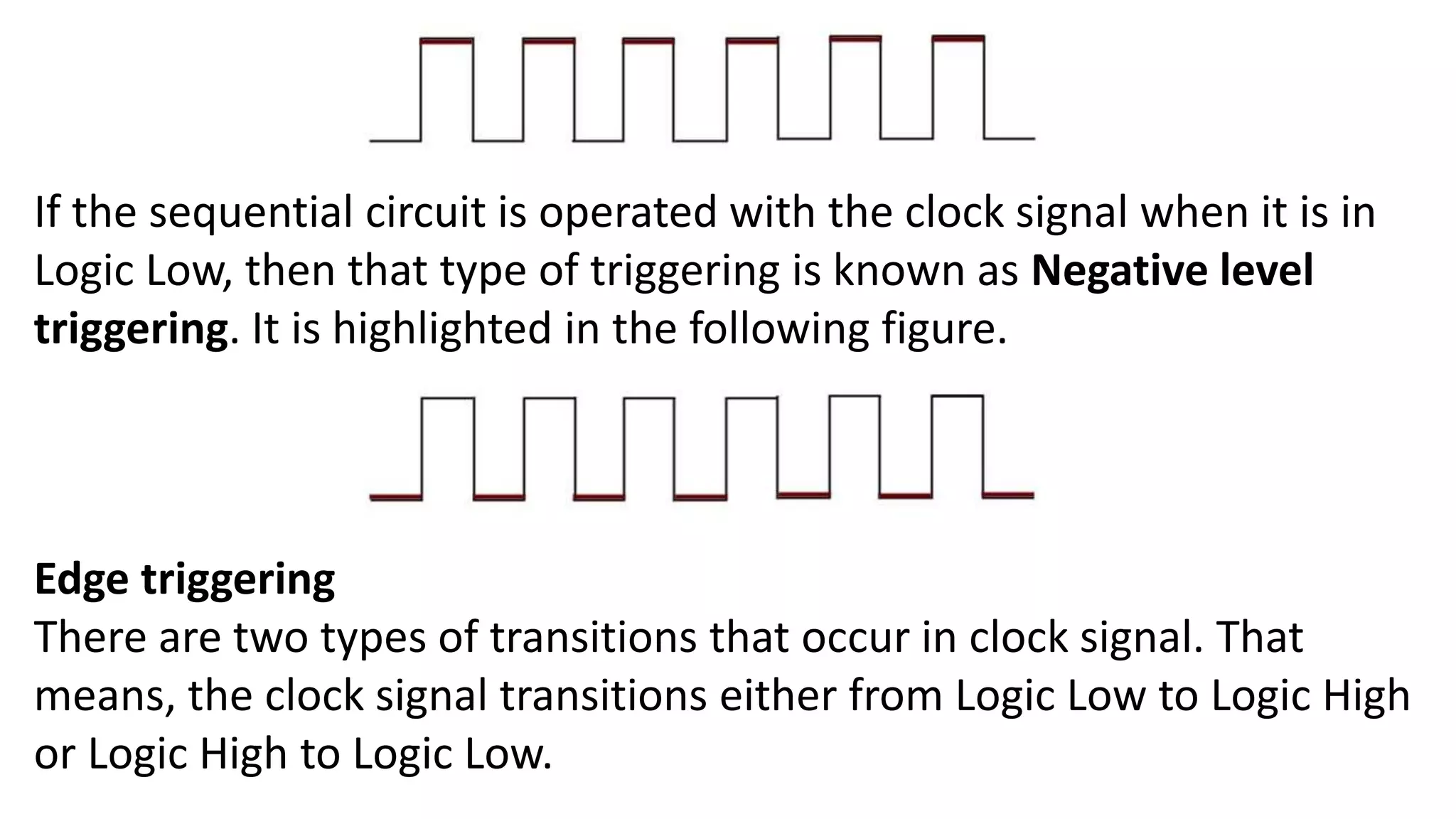
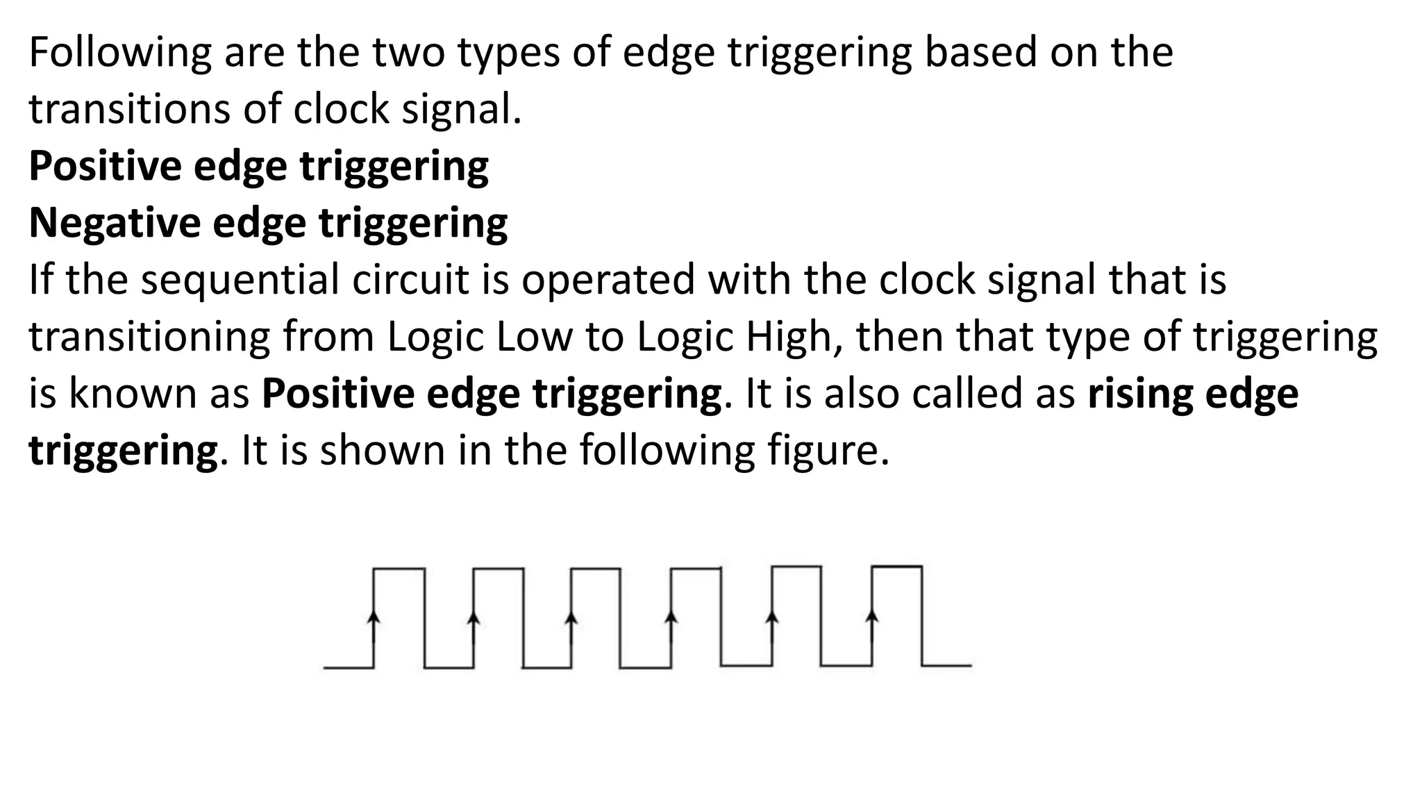
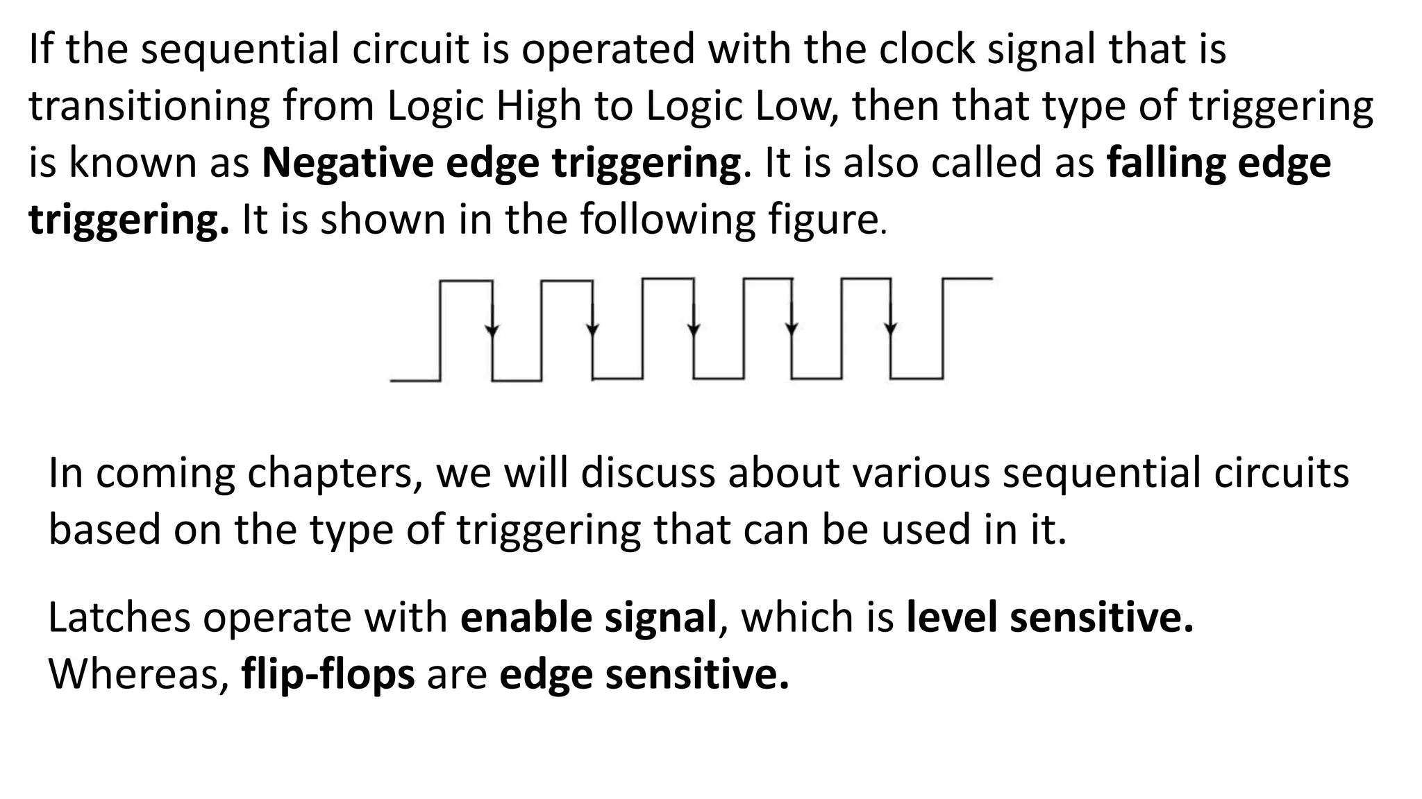
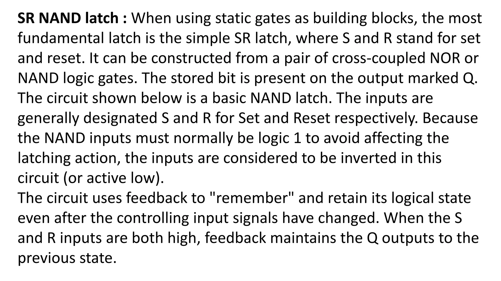
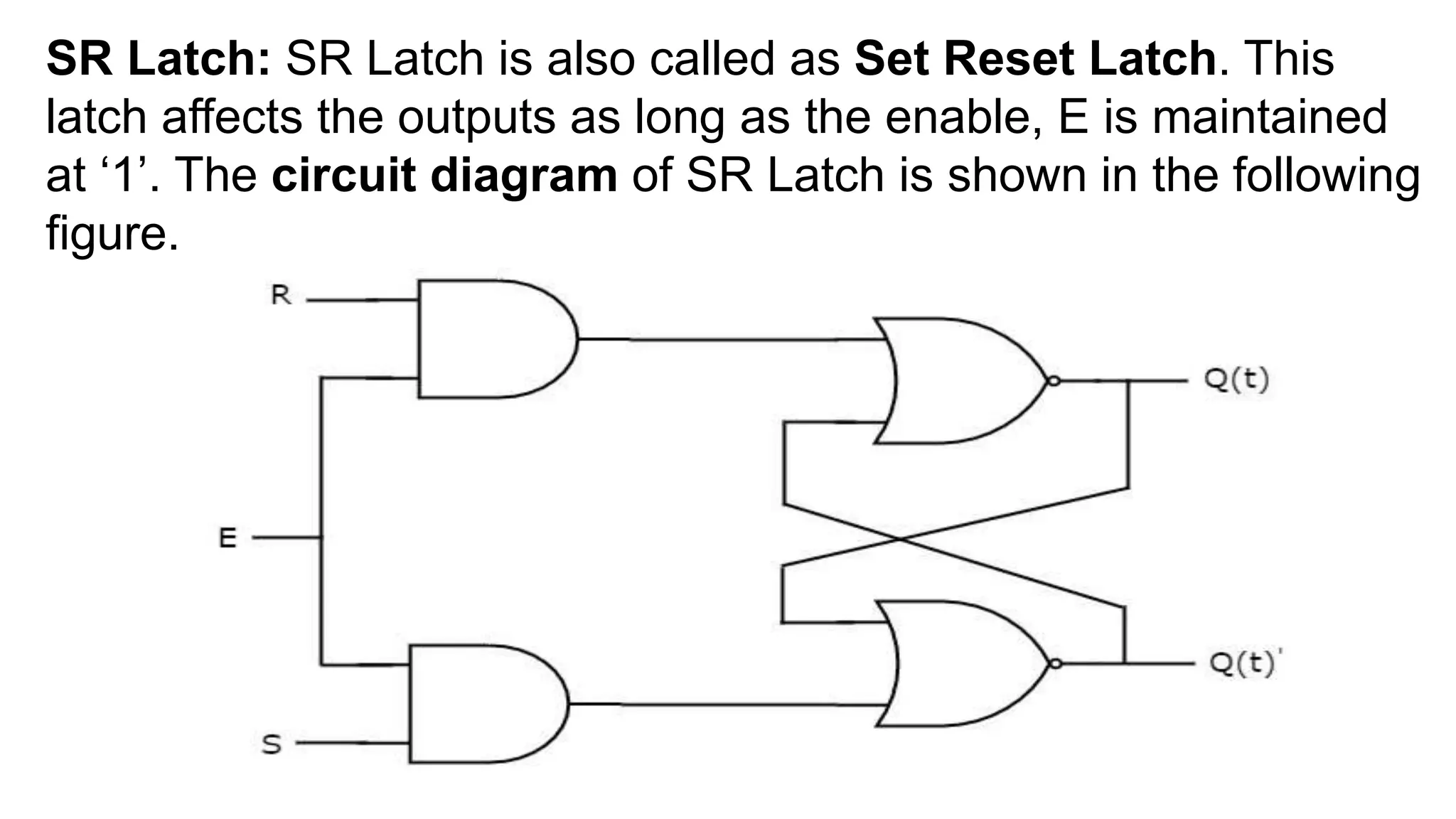
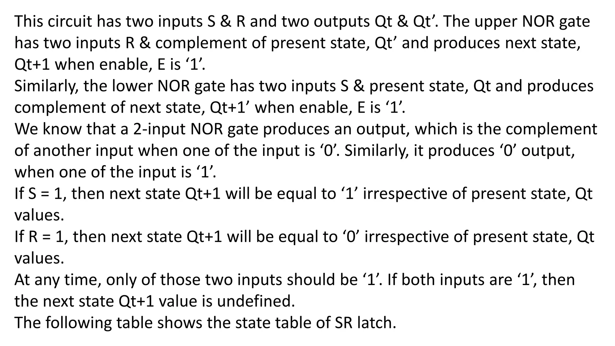
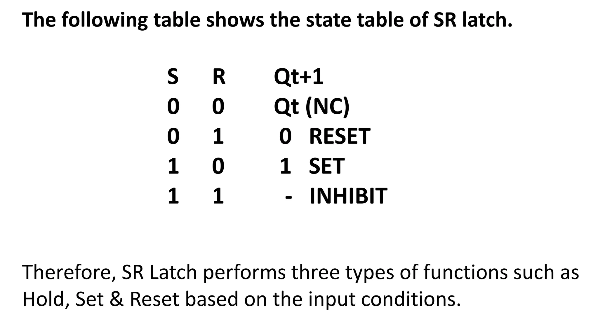
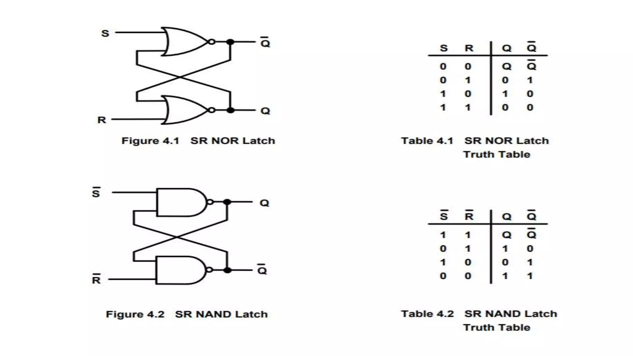
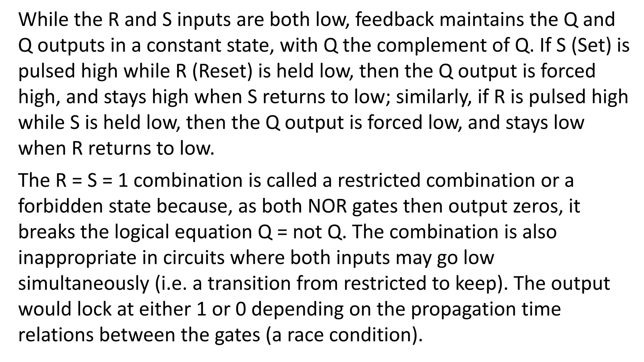
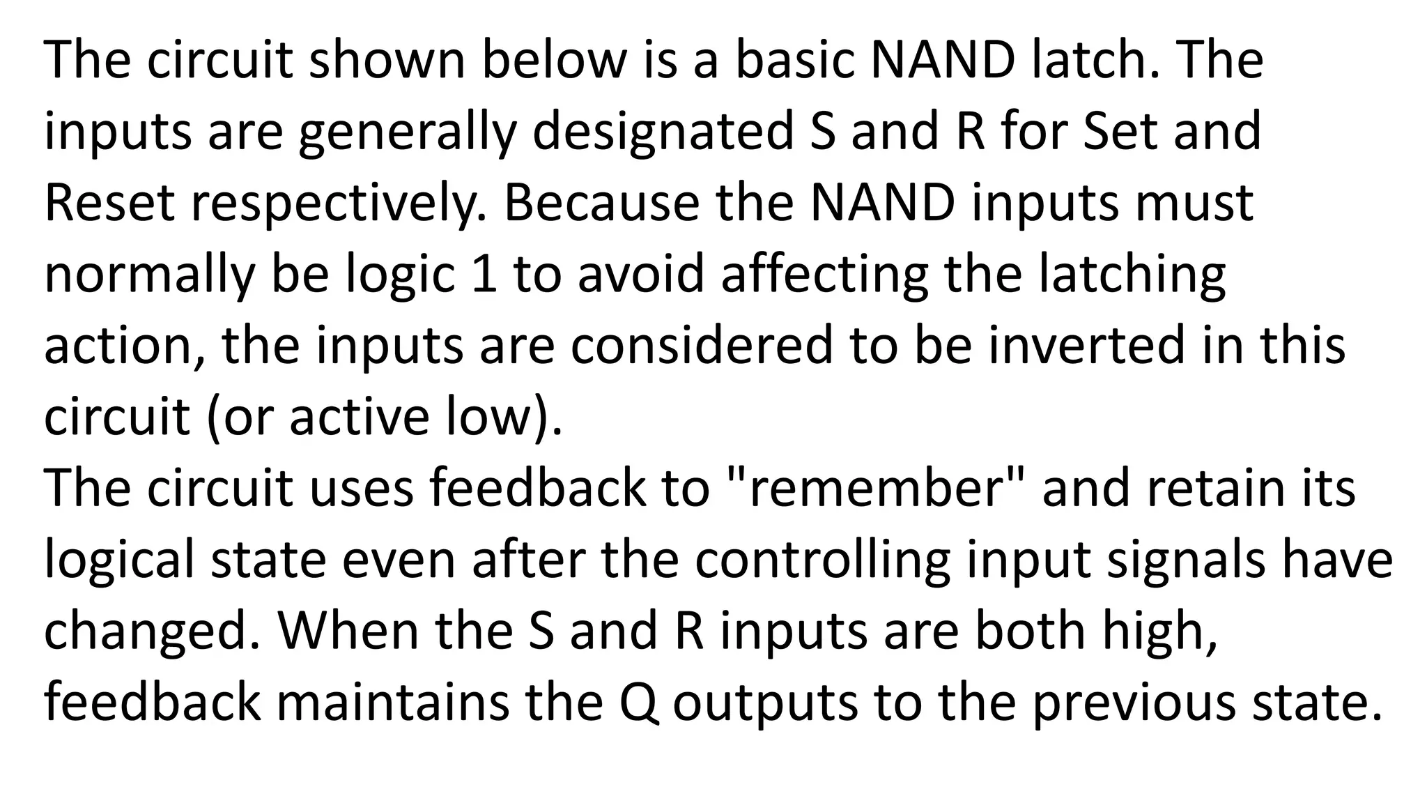
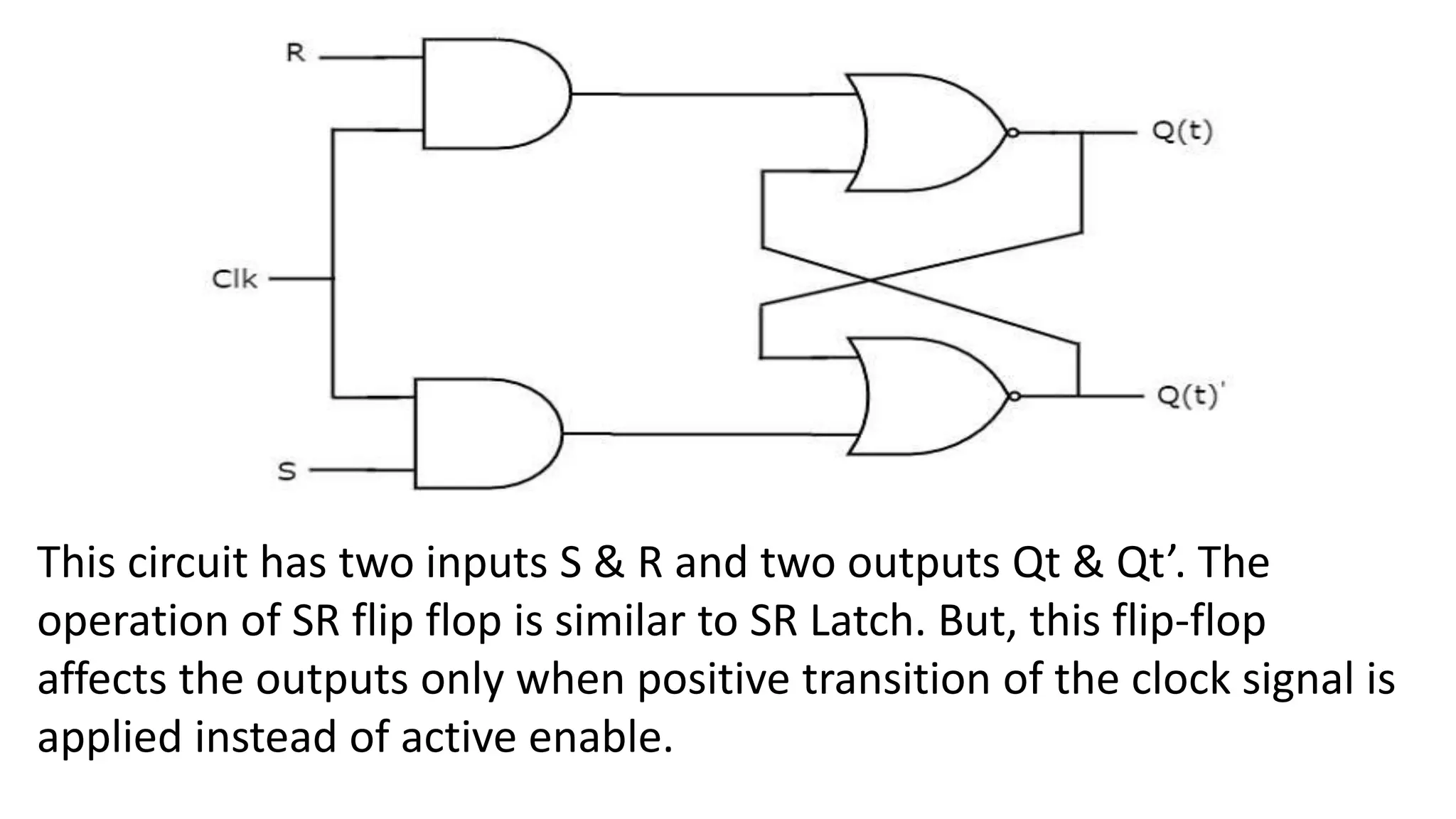
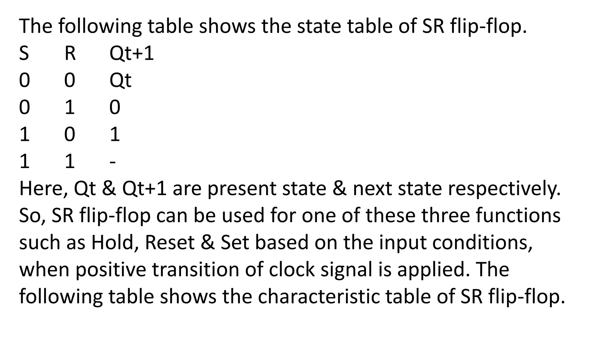
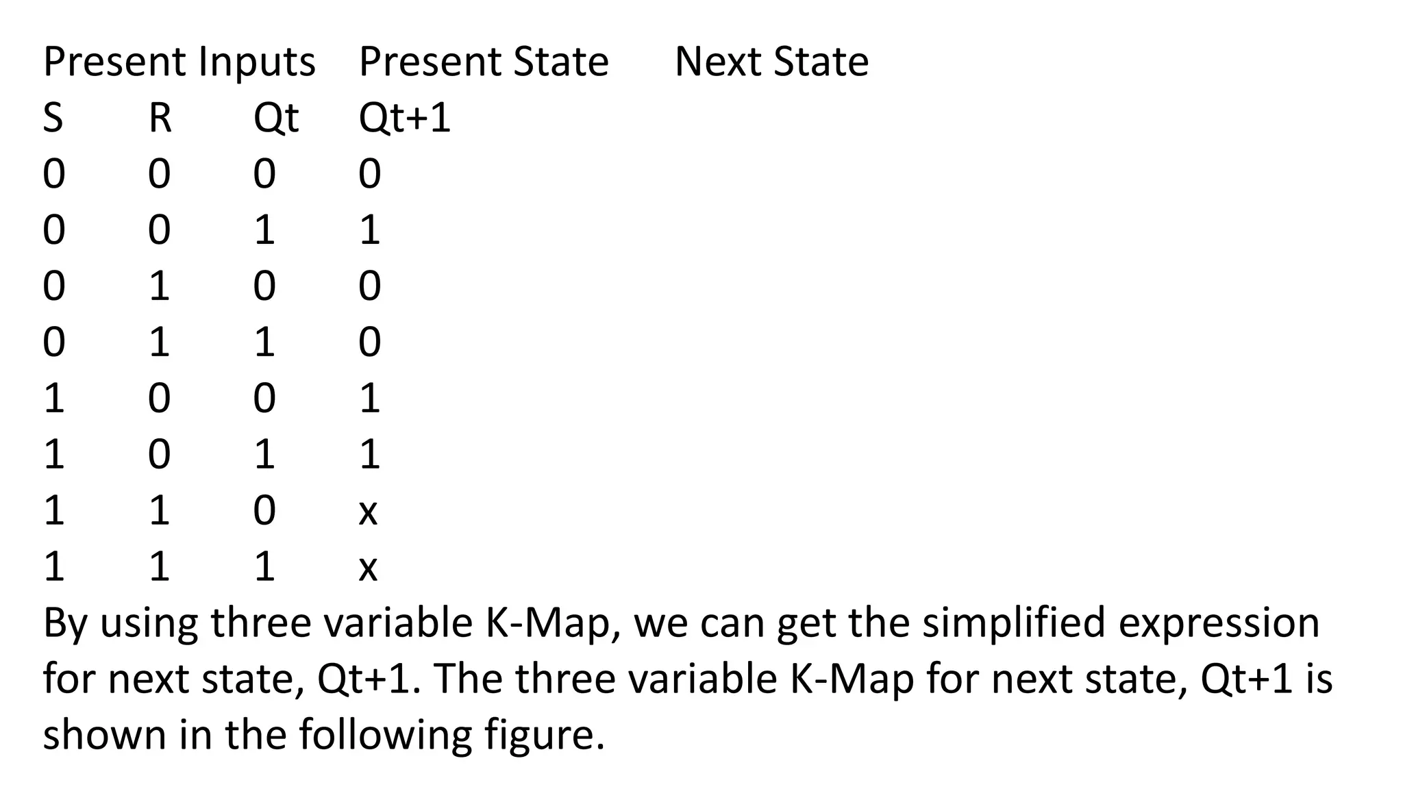
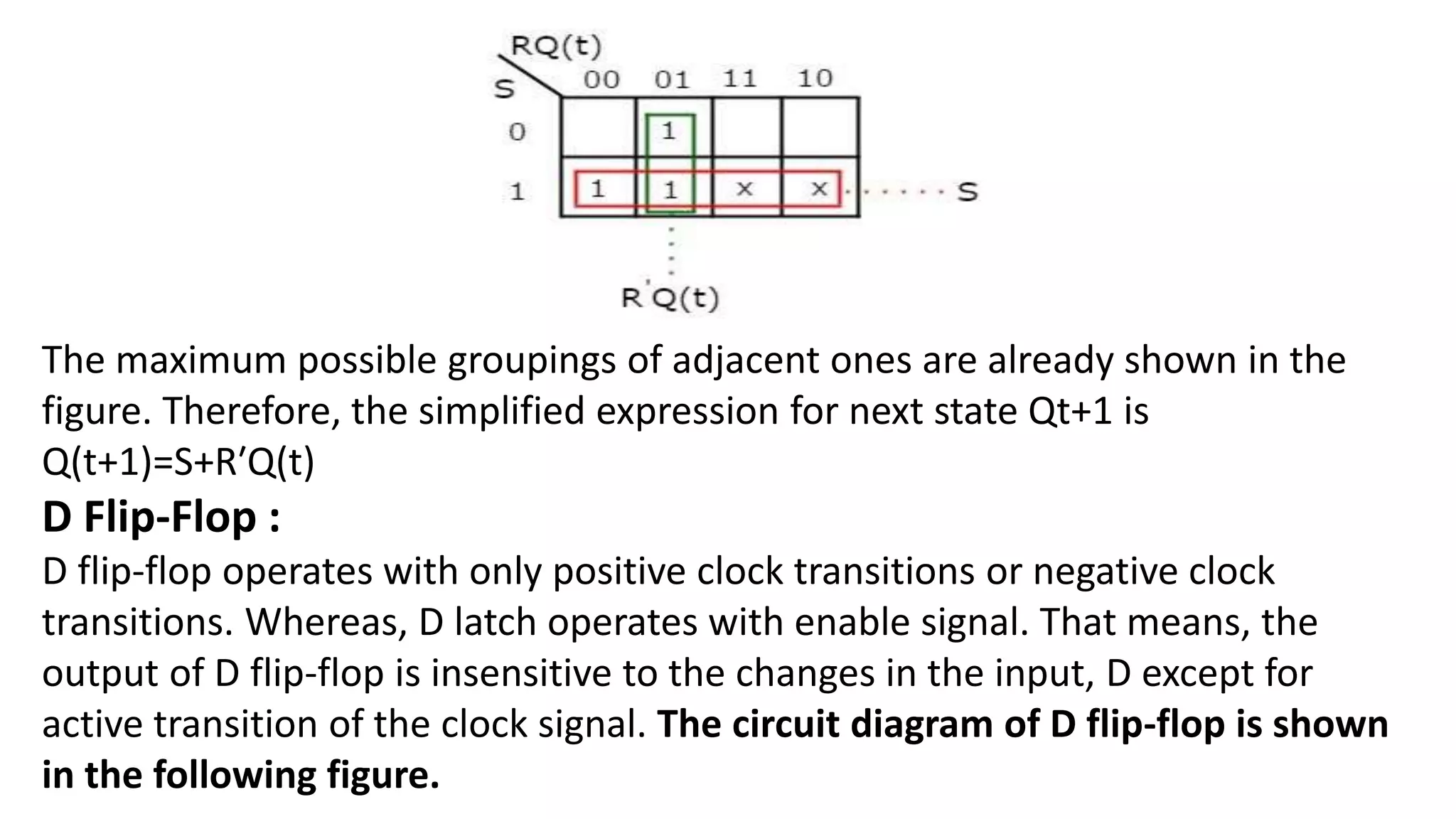
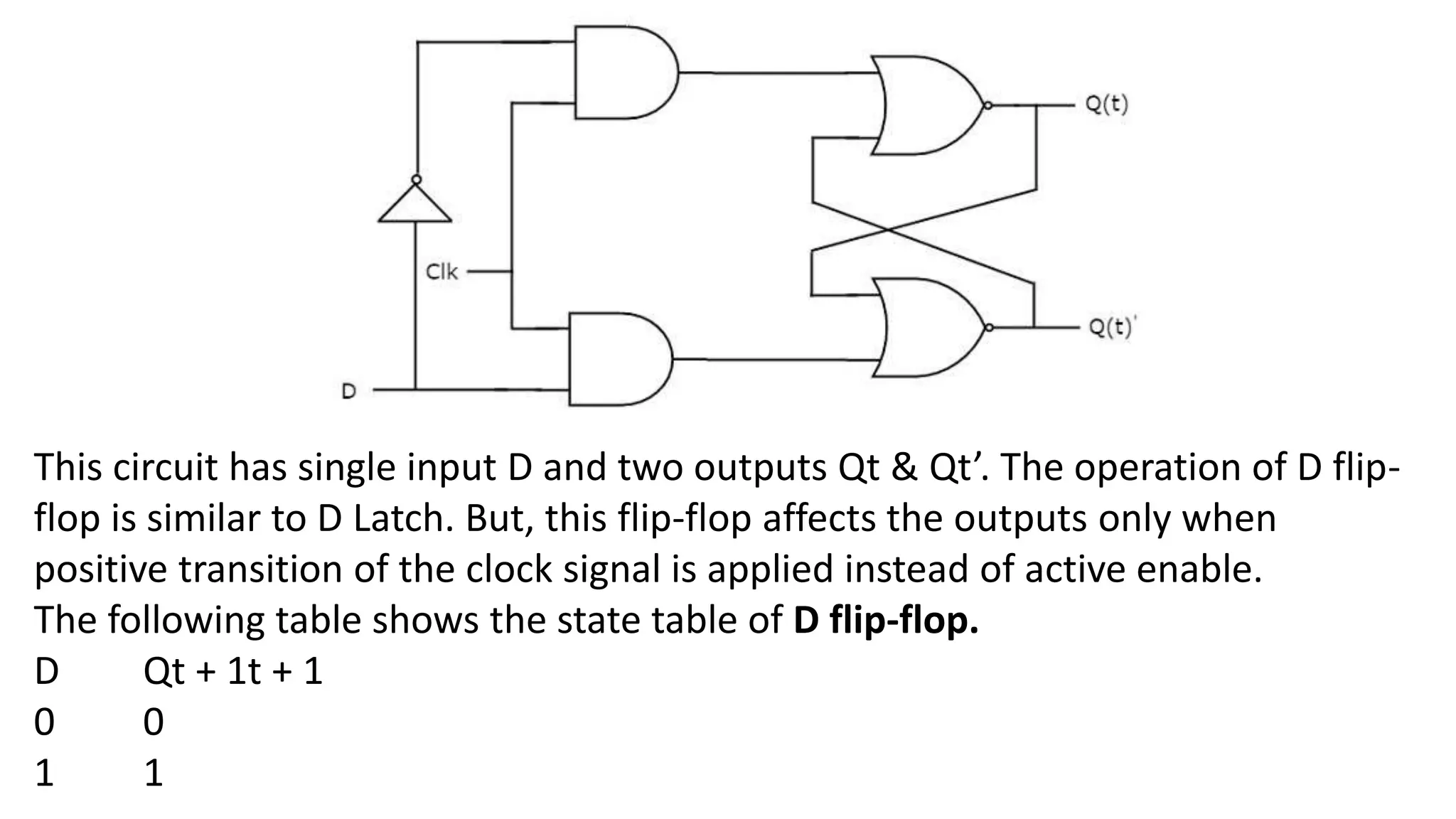
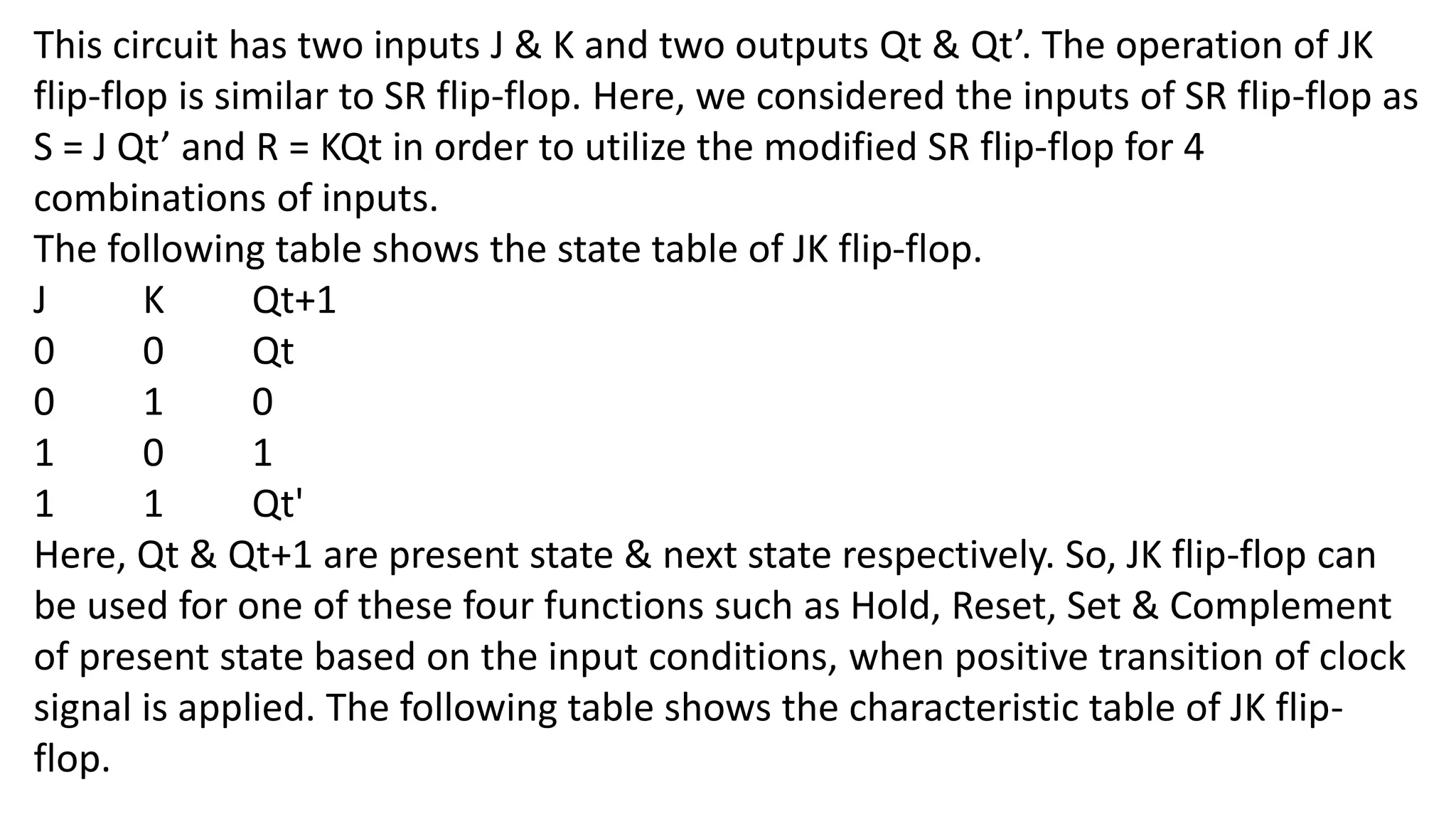
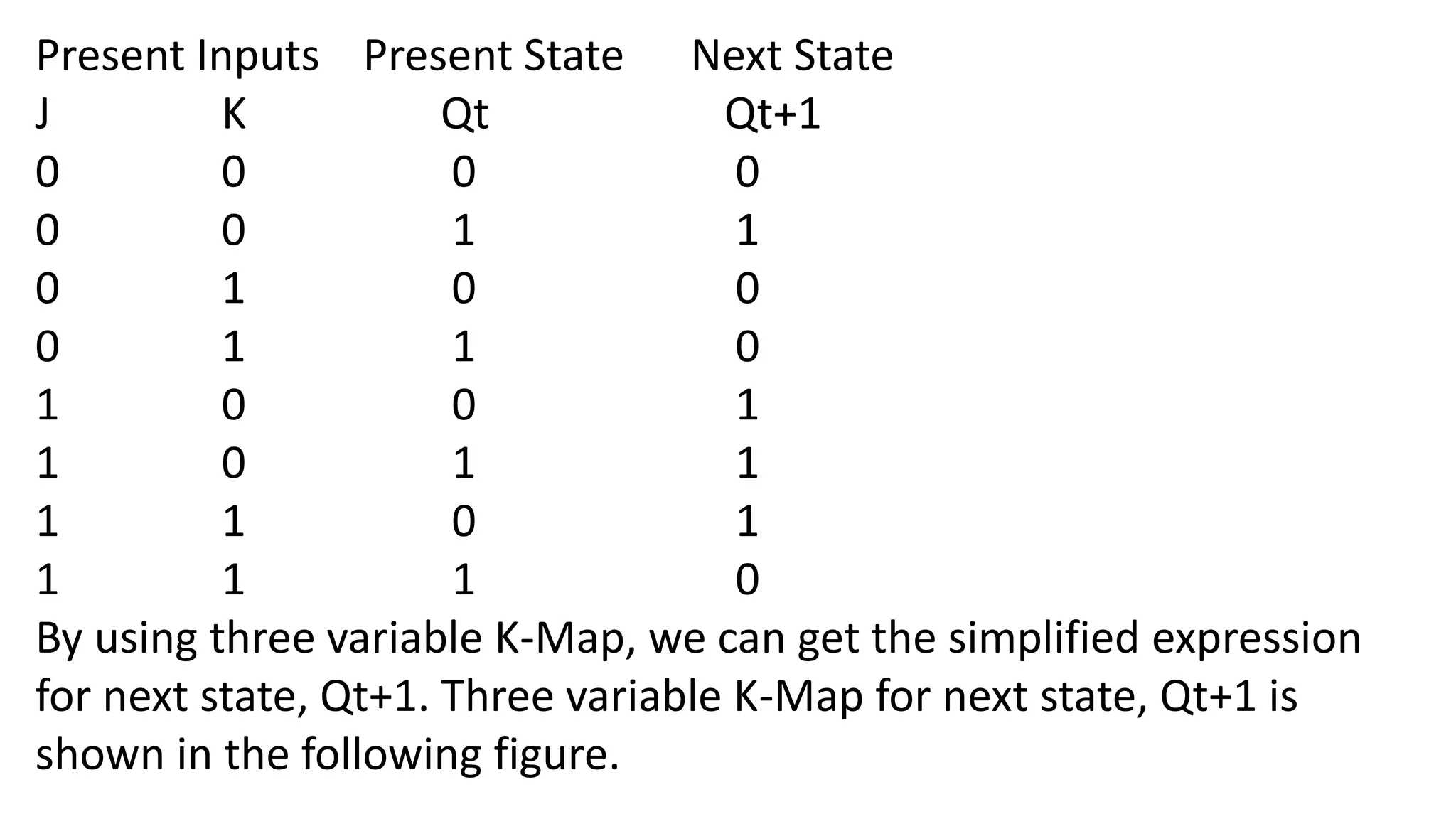
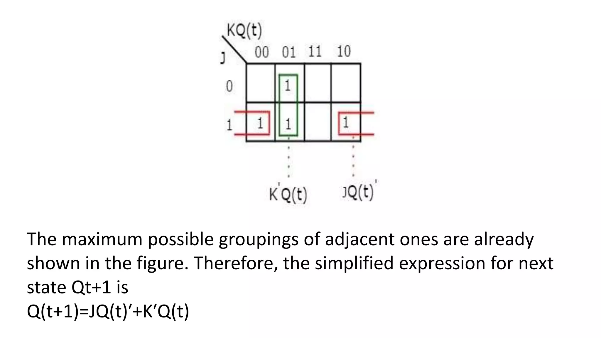
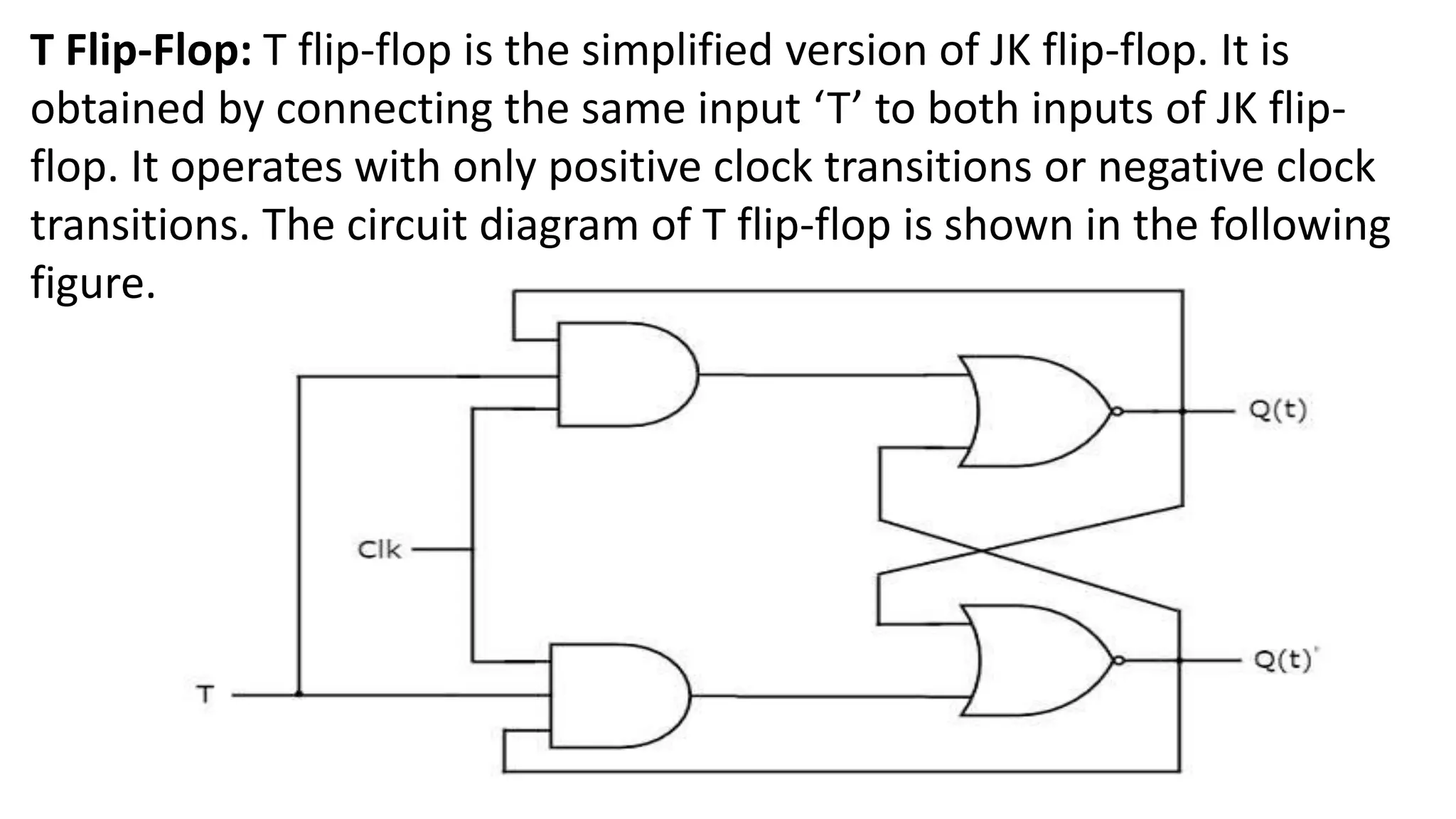
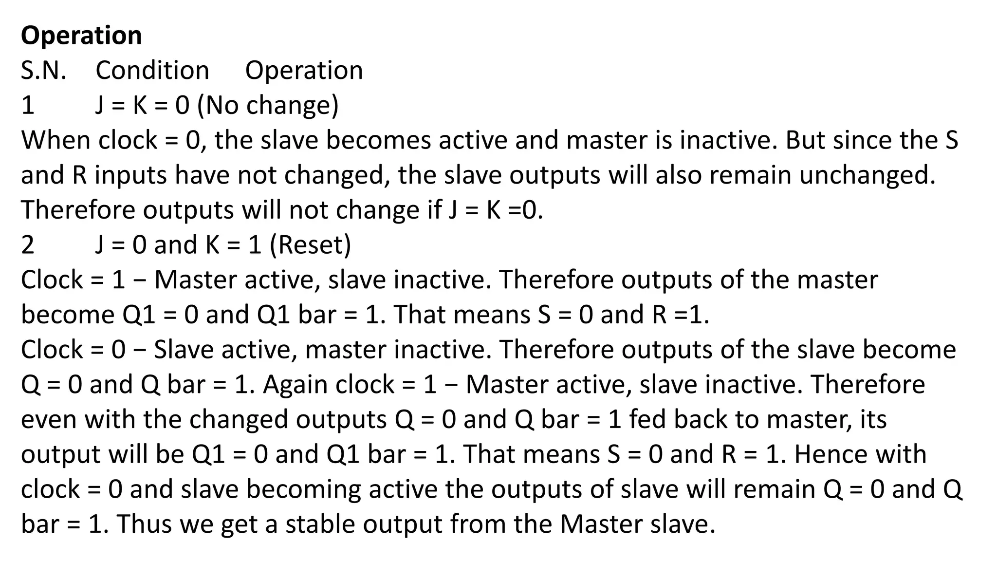
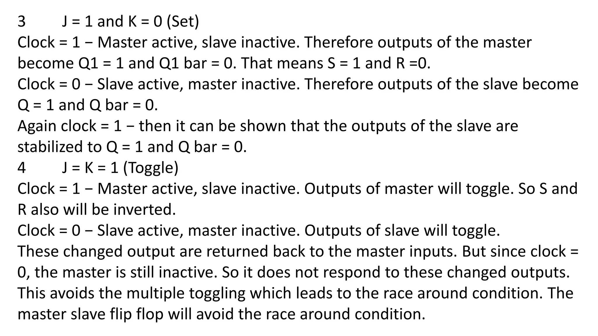
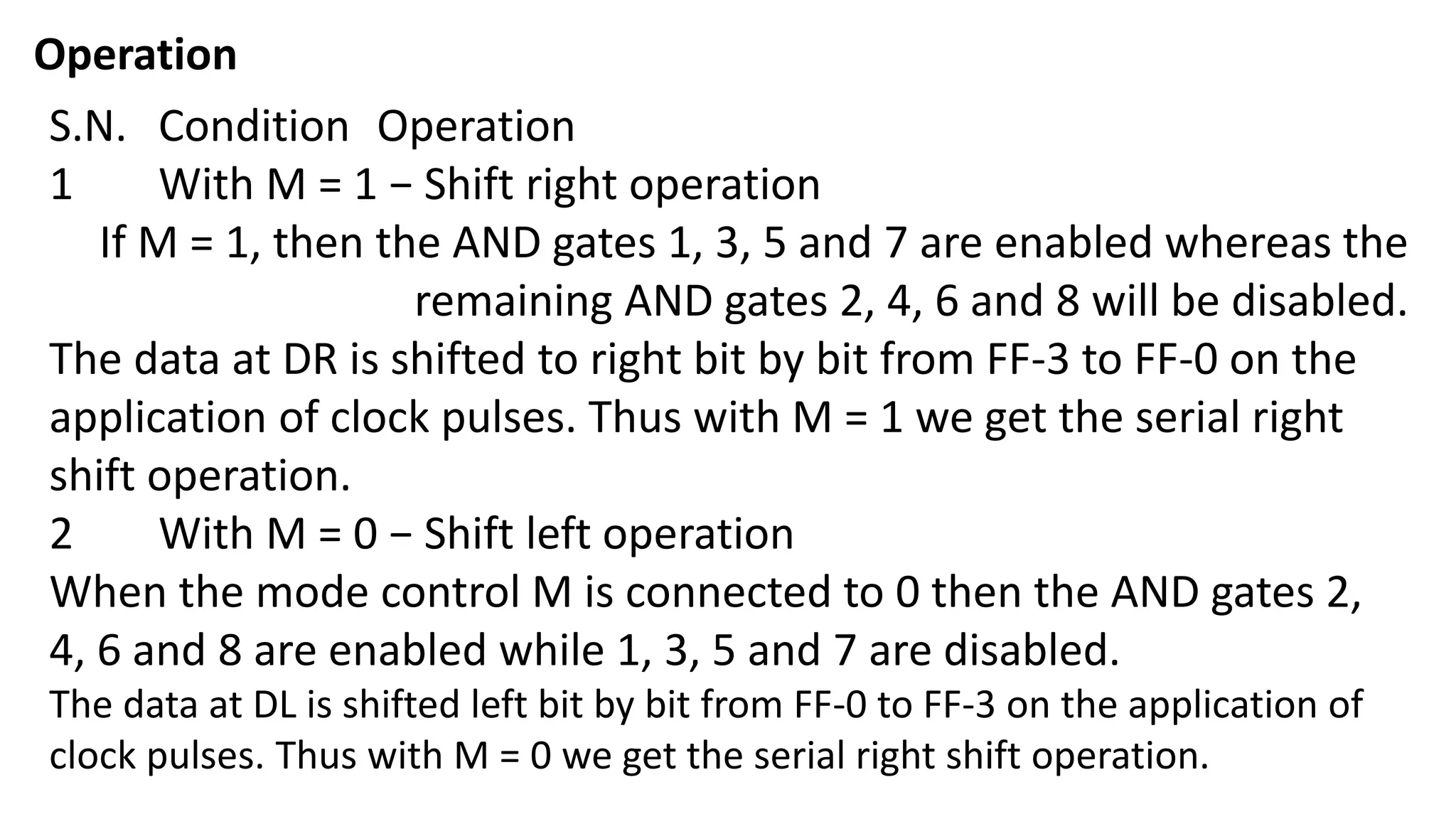
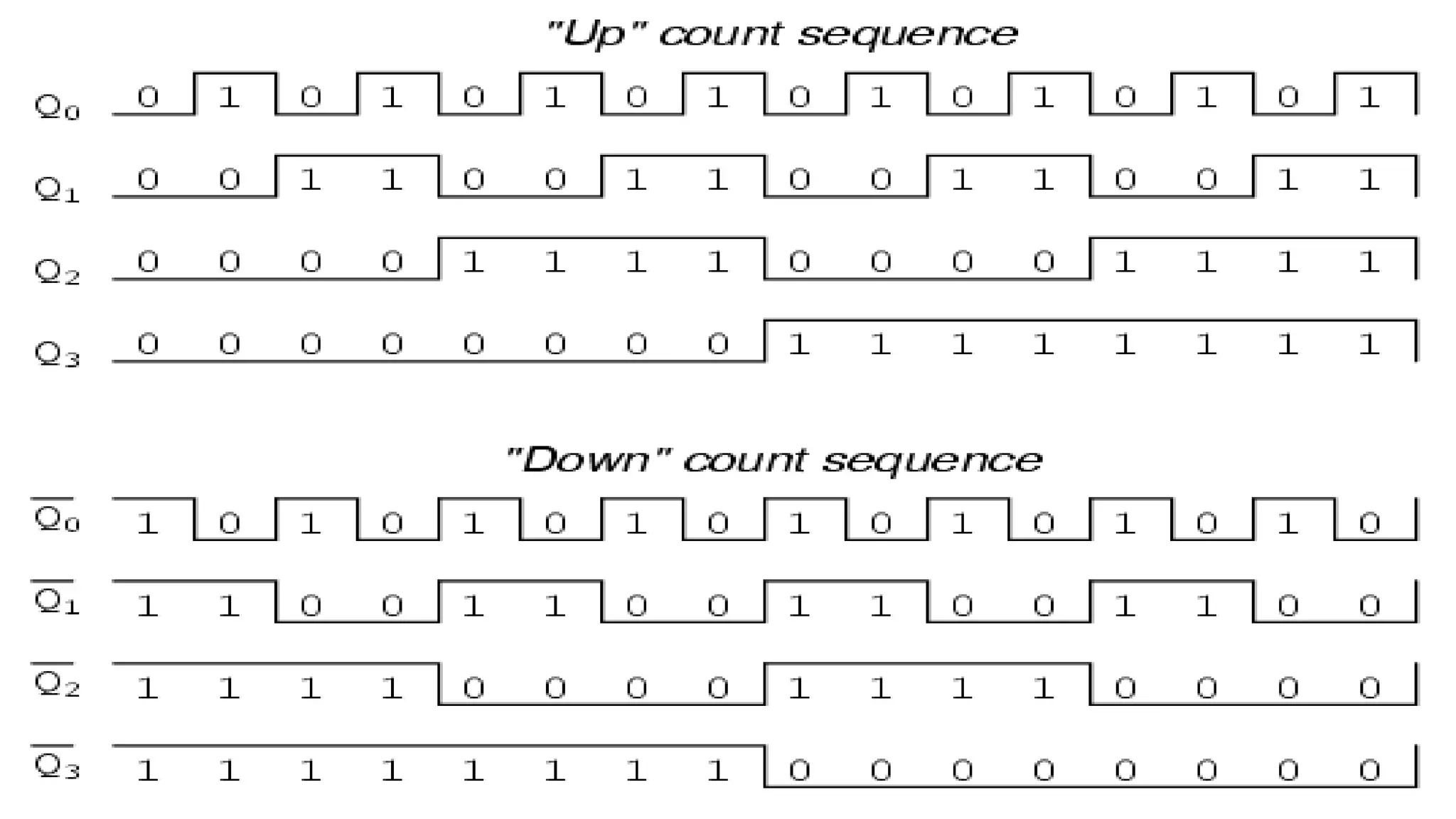
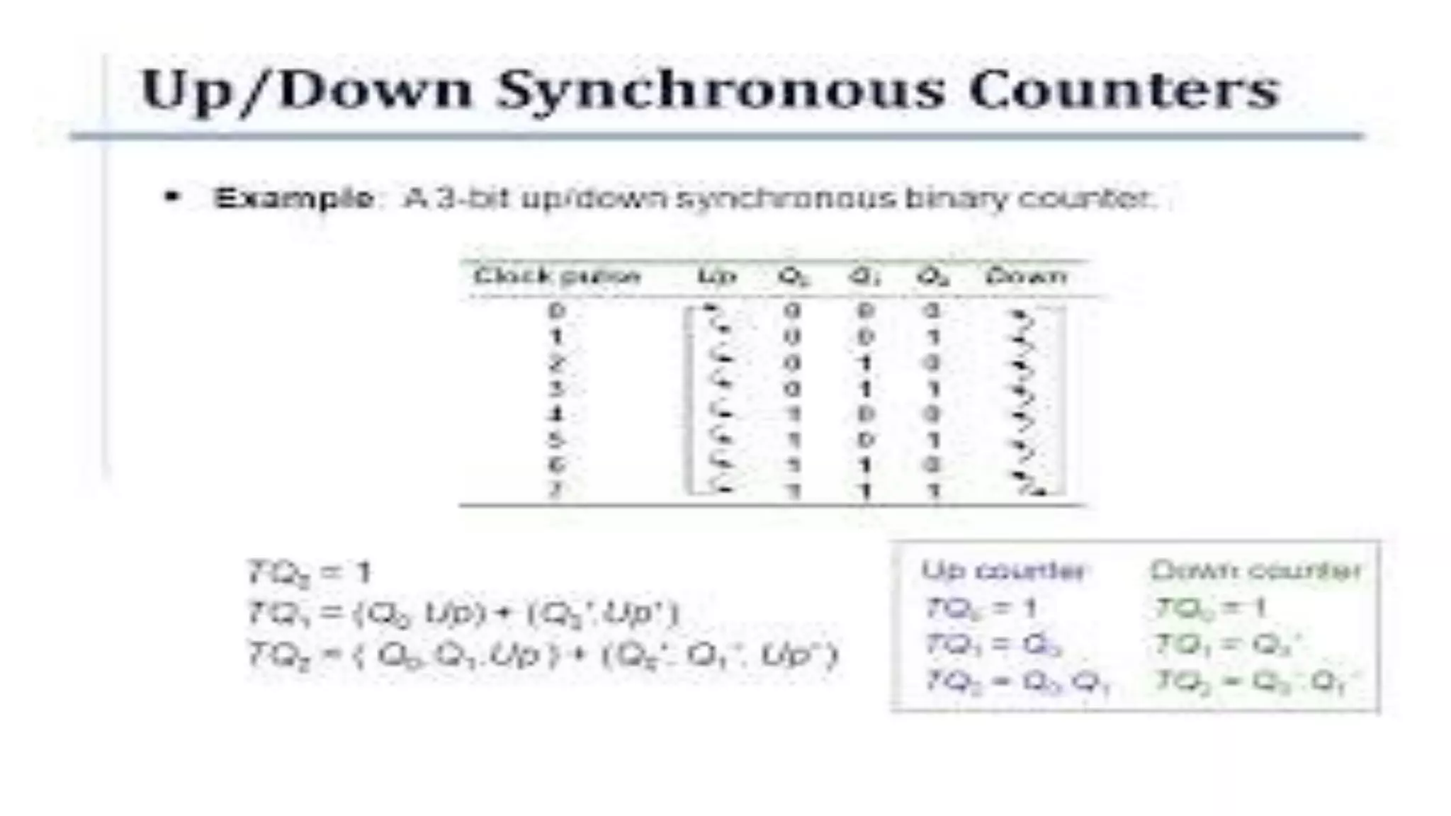
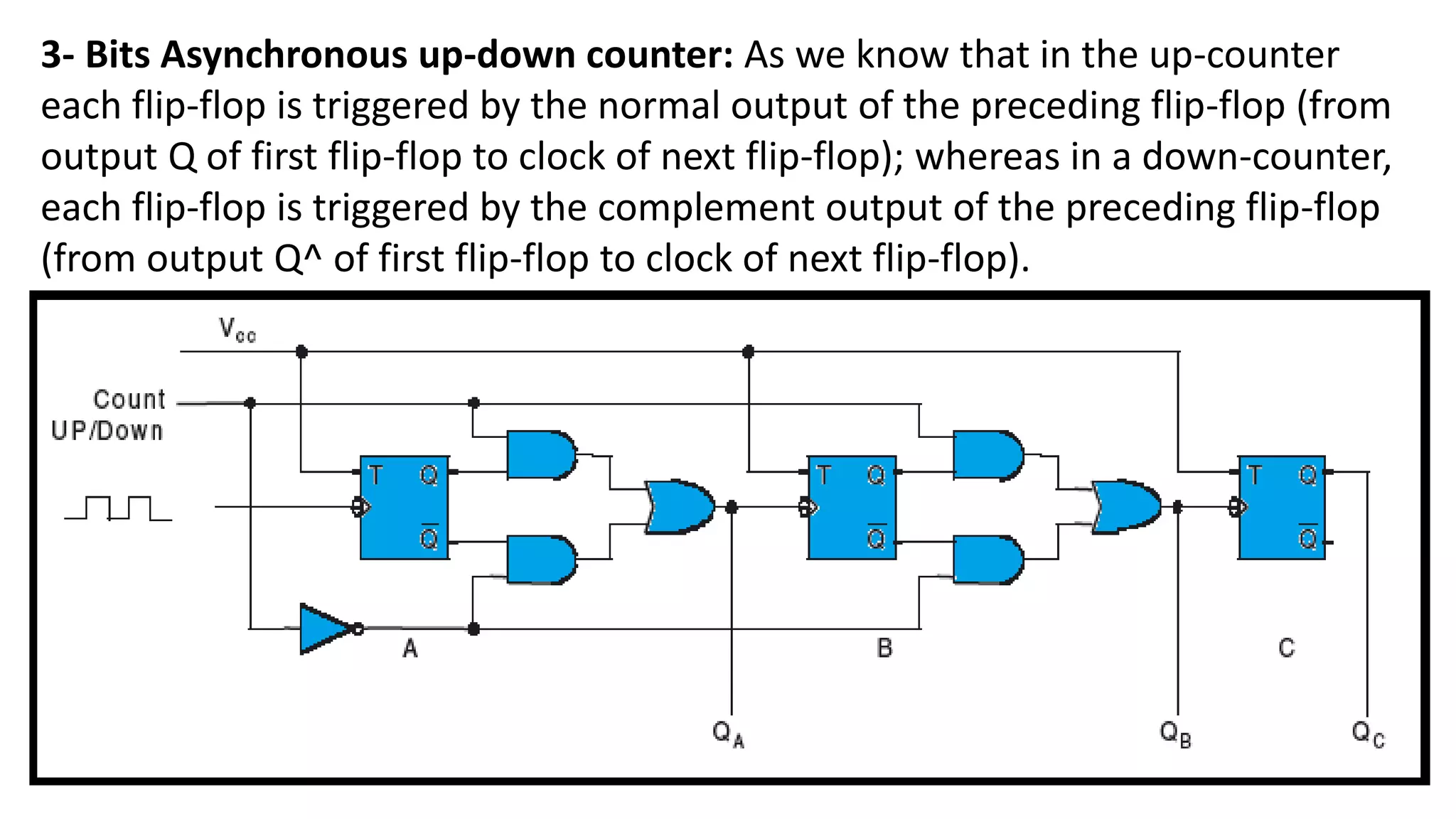
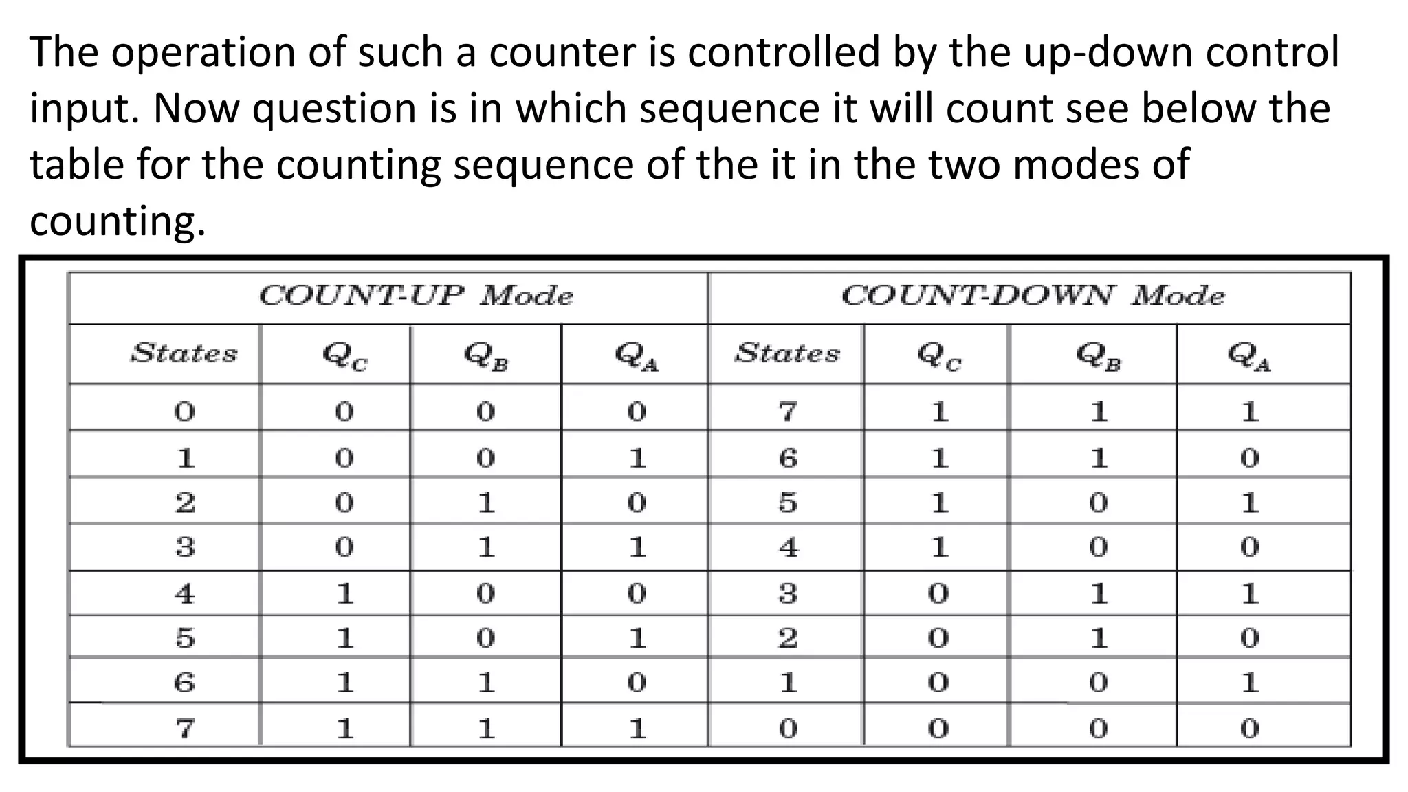
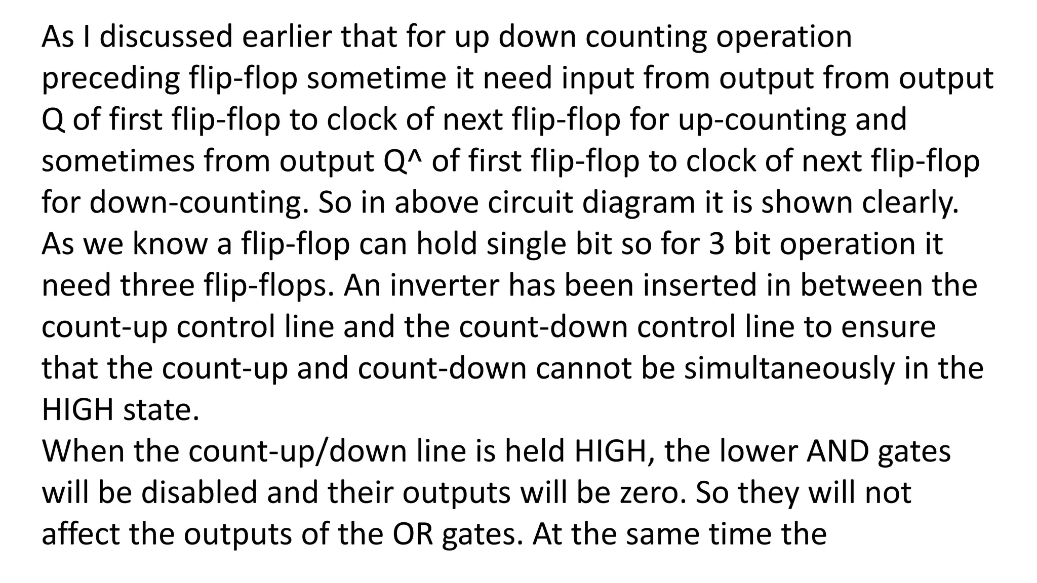
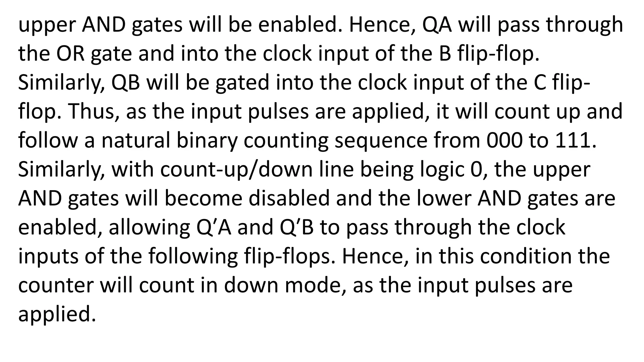
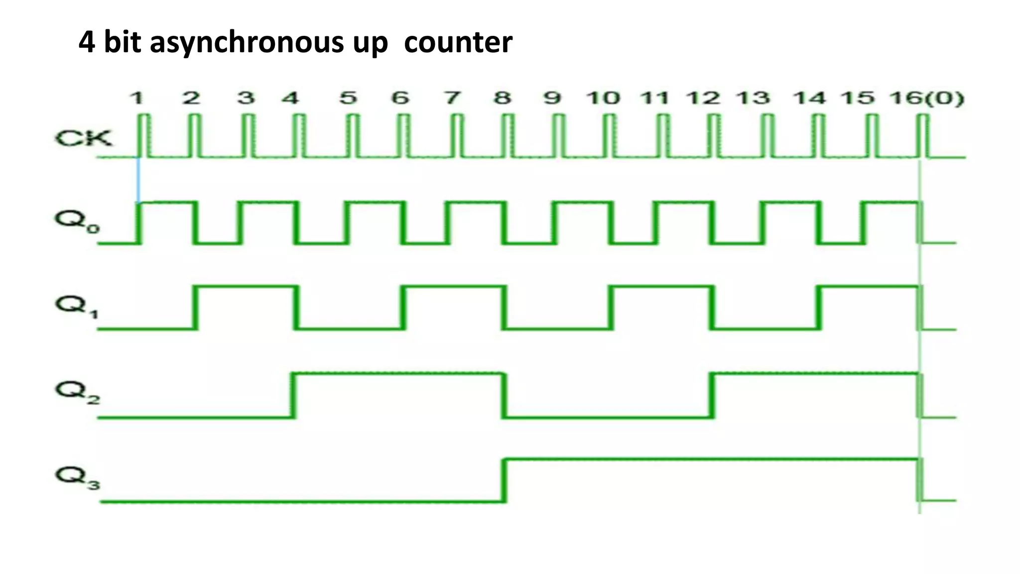
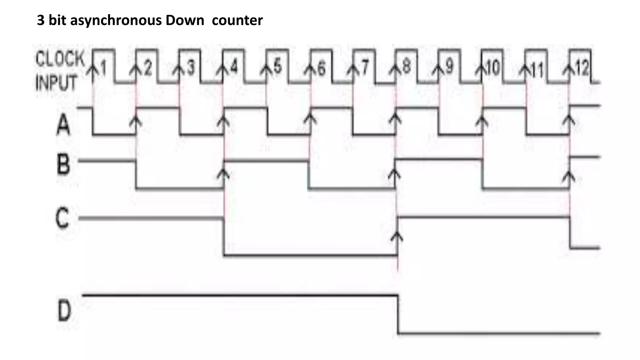
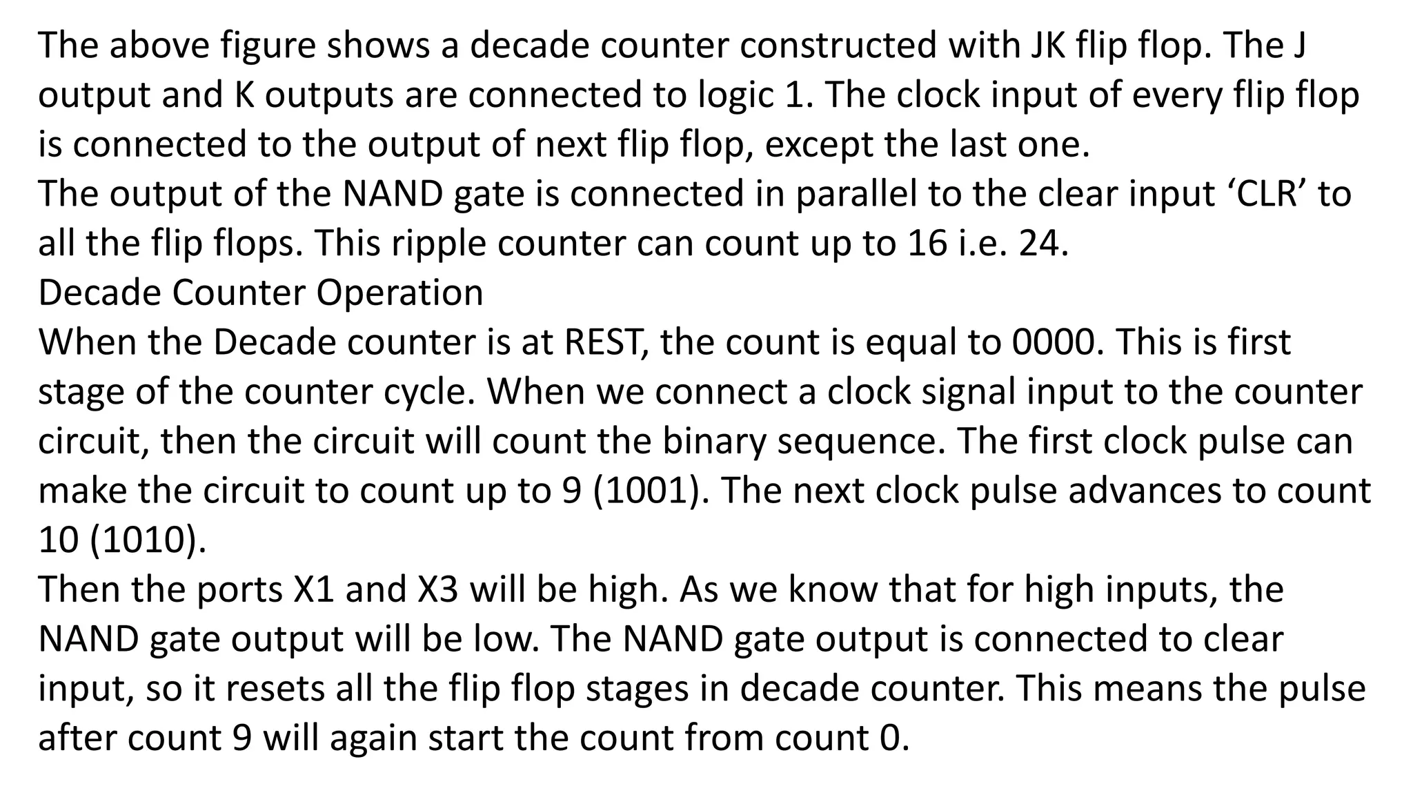
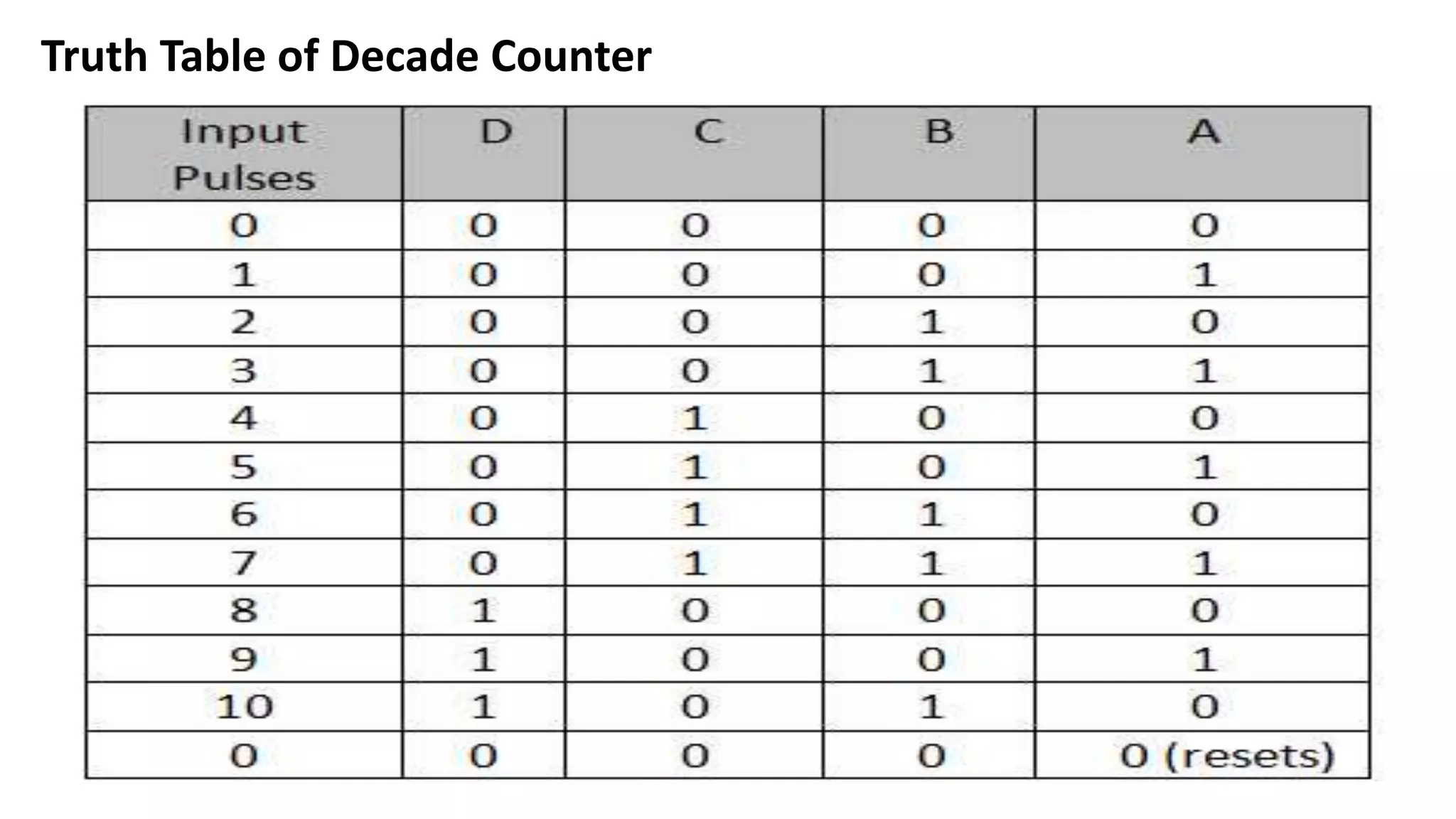
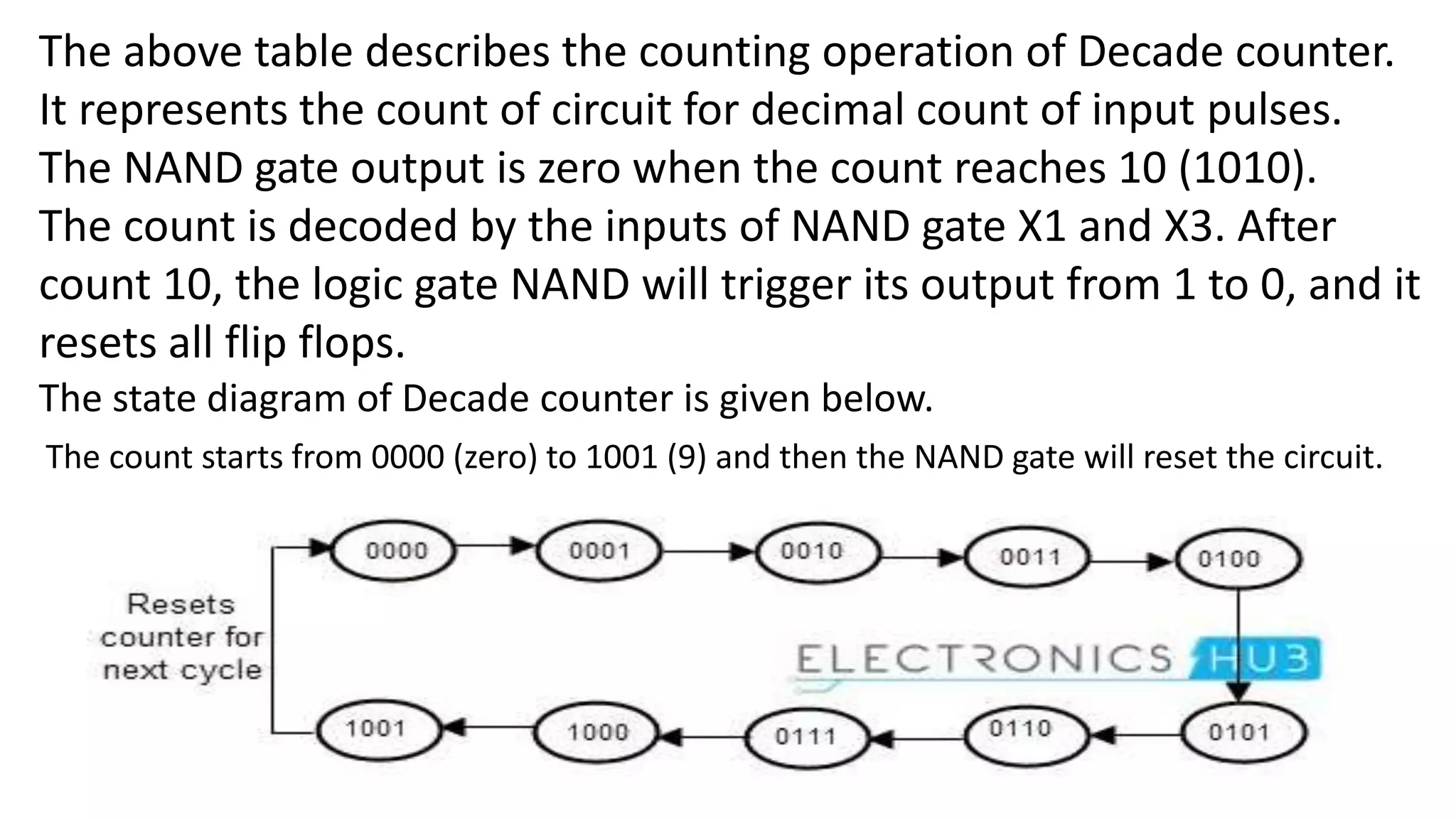
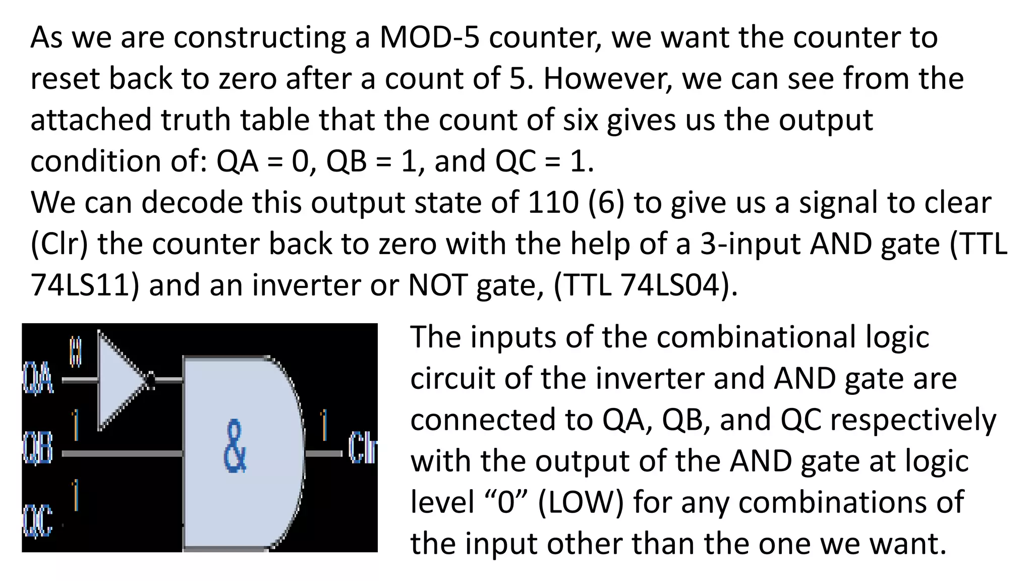
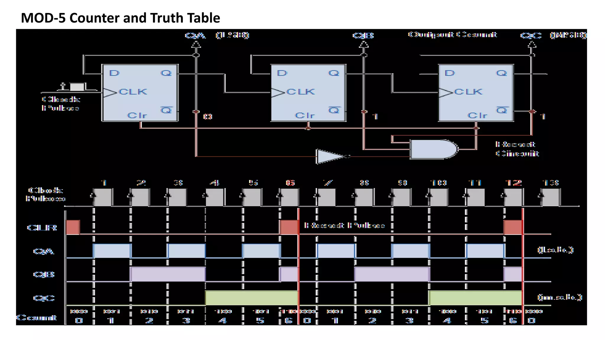
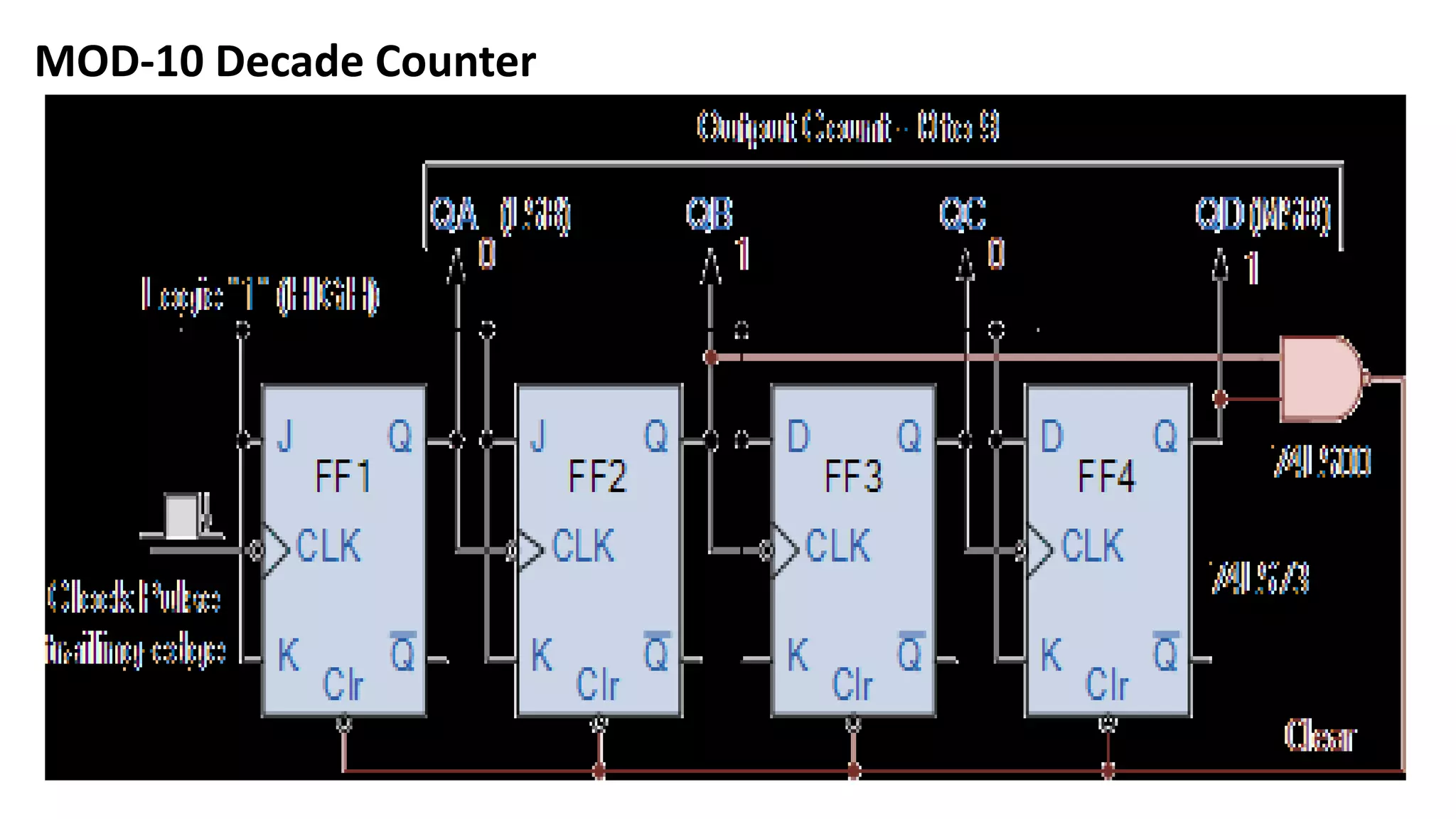
1. The document discusses sequential logic circuits and various types of flip-flops including SR, D, JK, and T flip-flops. It explains the operation of each flip-flop through truth tables and timing diagrams.
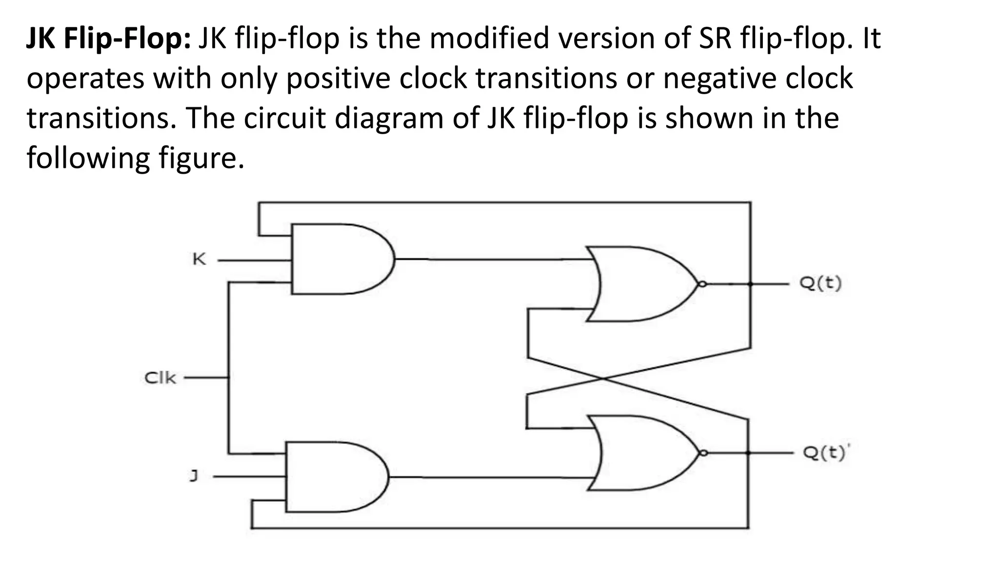
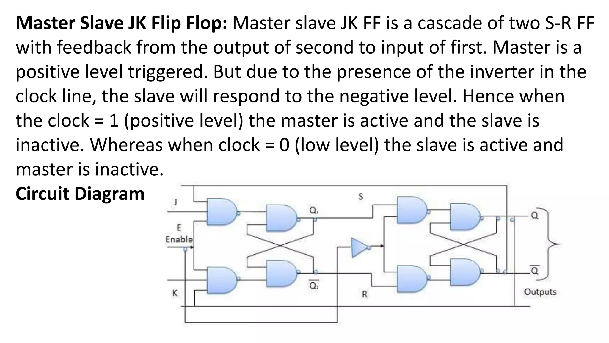
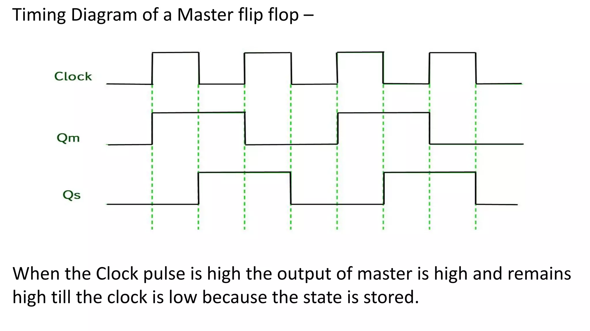
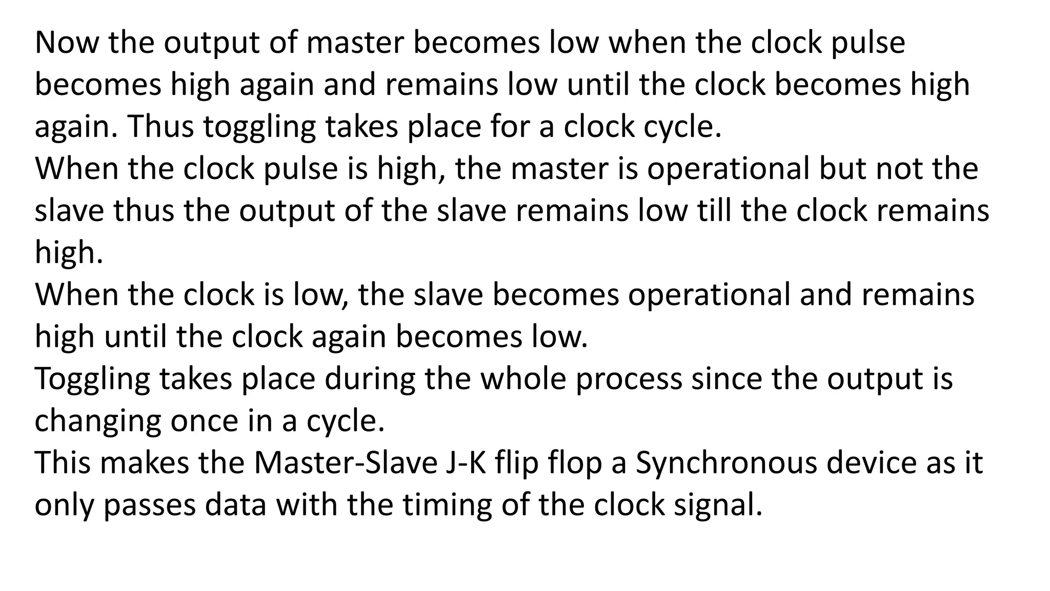
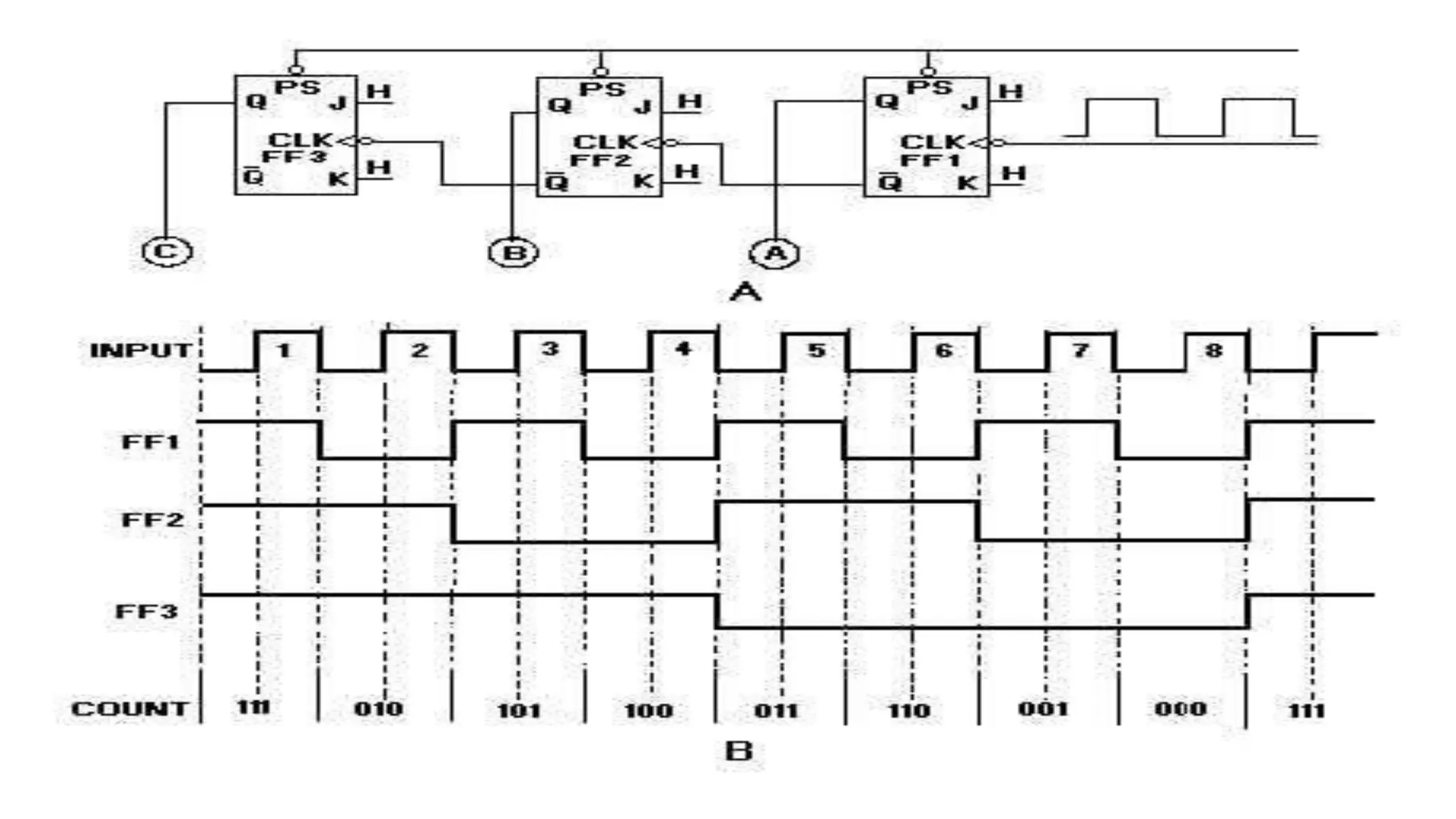
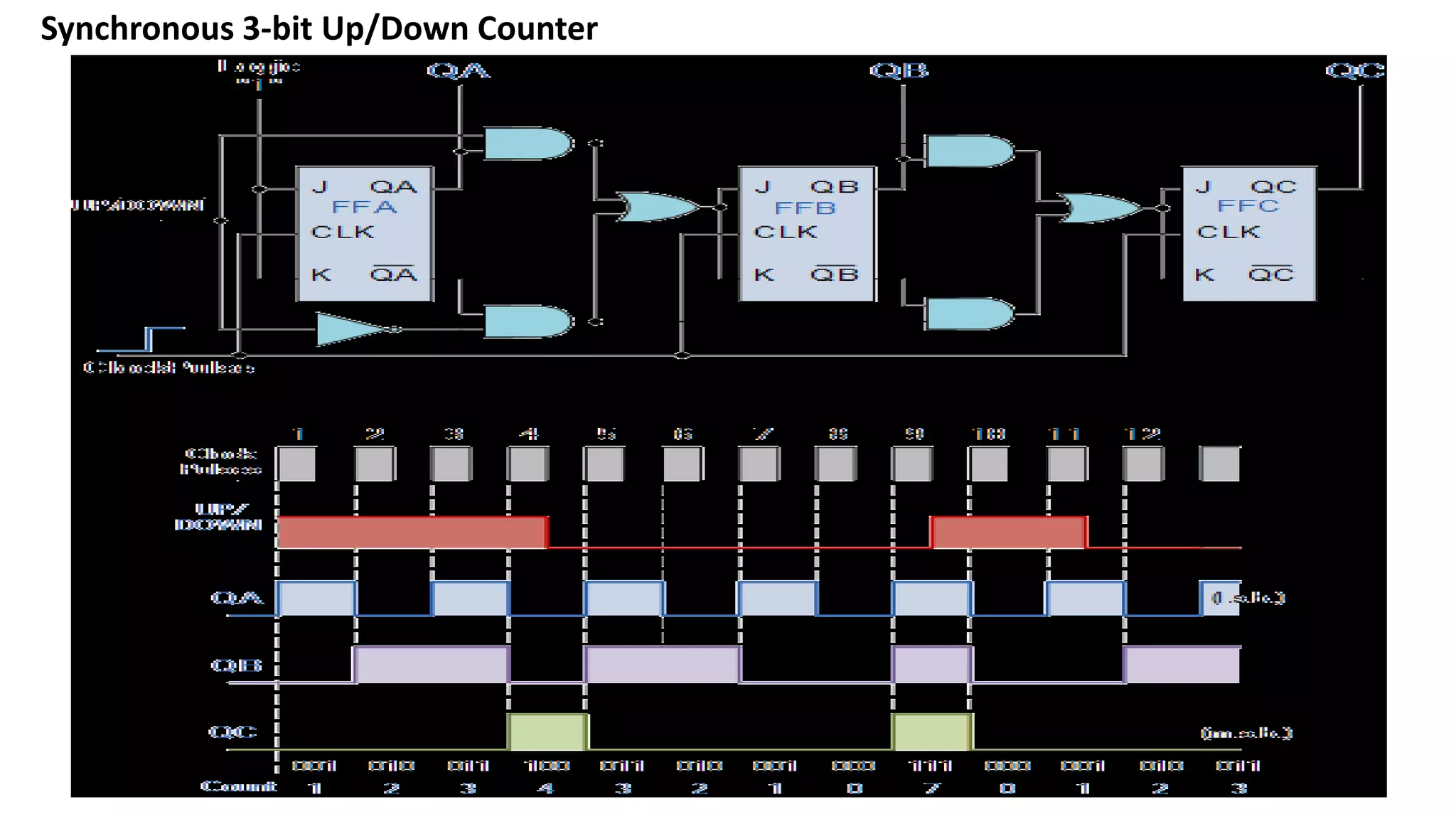
2. Master-slave JK flip-flops are described as using two SR flip-flops in a cascade configuration to avoid unwanted output changes from glitches in the clock signal.
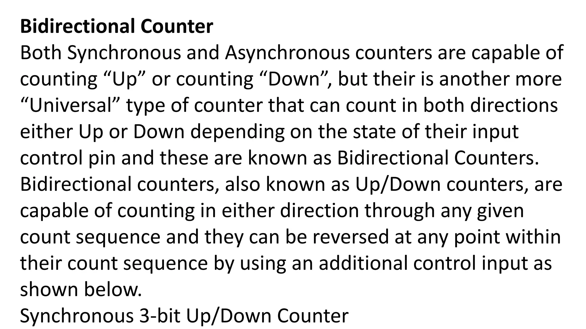
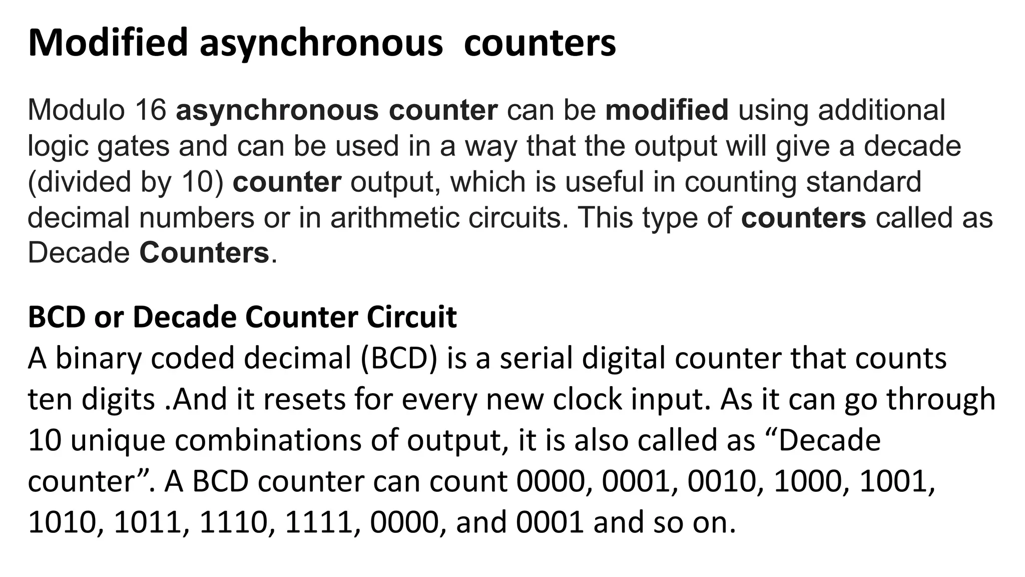
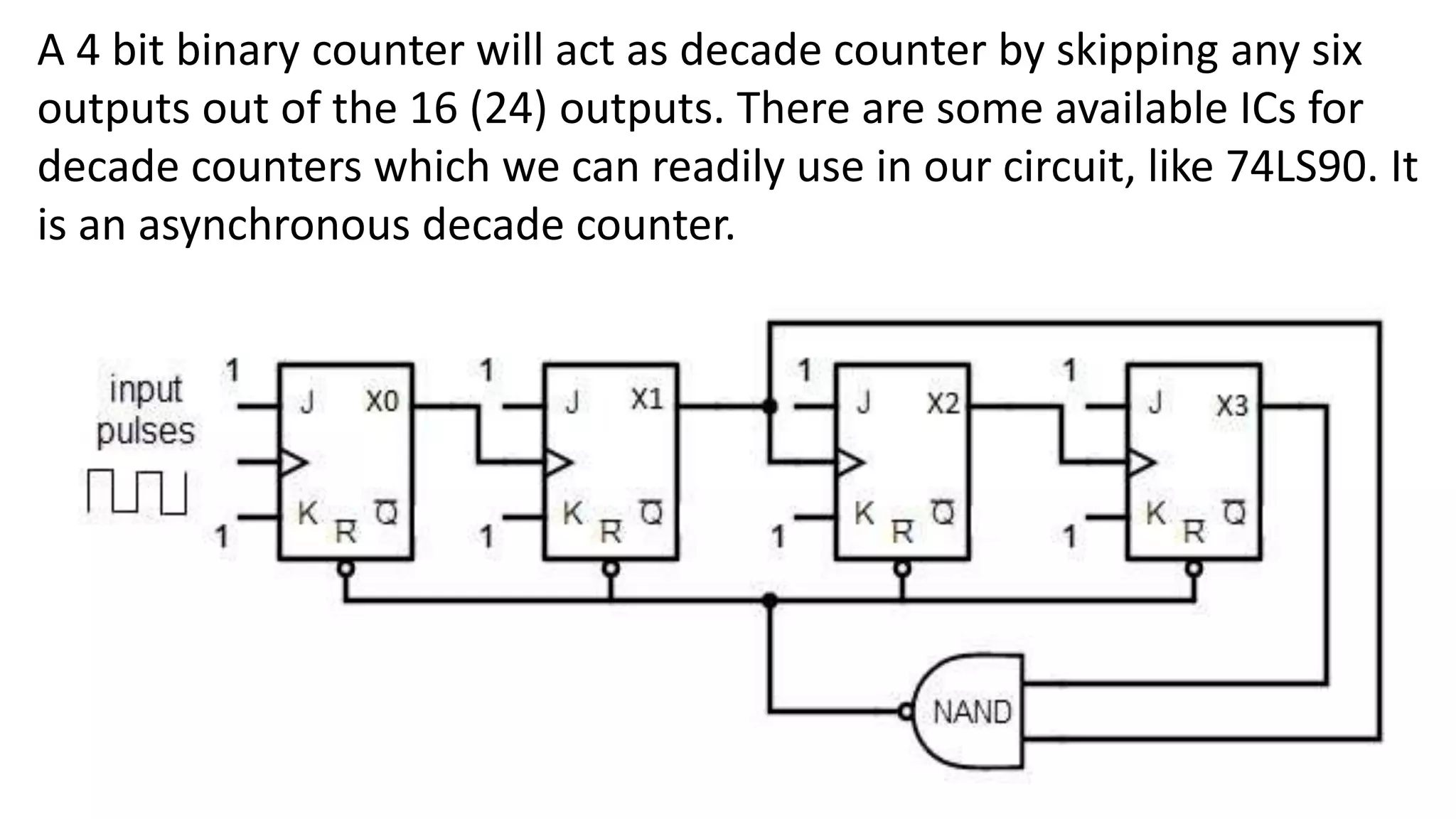
3. Other topics covered include latches, triggering methods, and uses of different flip-flop types in applications such as registers and counters.