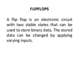
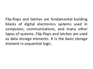
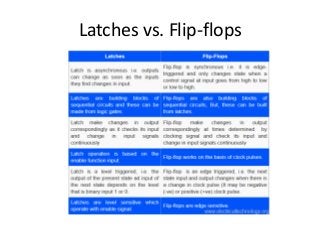
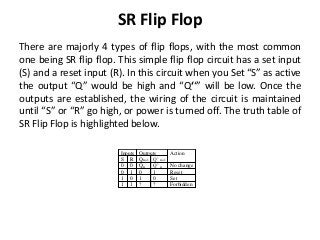
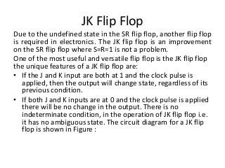
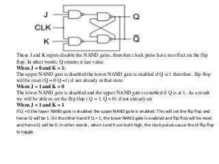
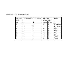
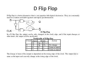
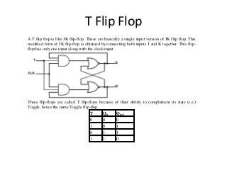
FLIPFLOPS
A flip flop is an electronic circuit
with two stable states that can be
used to store binary data. The stored
data can be changed by applying
varying inputs.
Flip-flops and latches are fundamental building
blocks of digital electronics systems used in
computers, communications, and many other
types of systems. Flip-flops and latches are used
as data storage elements. It is the basic storage
element in sequential logic.
Latches vs. Flip-flops
SR Latch using NAND gates
In this circuit when you Set S as active the output Q would be high and Q’
will be low.
SR Flip-Flop using NAND gates
In this circuit diagram, the output is changed (i.e. the stored data is changed) only when you give
an active clock signal. Otherwise, even if the S or R is active the data will not change. Let’s look
at the types of flip-flops to understand better.
SR Flip Flop
There are majorly 4 types of flip flops, with the most common
one being SR flip flop. This simple flip flop circuit has a set input
(S) and a reset input (R). In this circuit when you Set “S” as active
the output “Q” would be high and “Q‘‘” will be low. Once the
outputs are established, the wiring of the circuit is maintained
until “S” or “R” go high, or power is turned off. The truth table of
SR Flip Flop is highlighted below.
Inputs Outputs Action
S R Qn+1 Q’ n+1
0 0 Qn Q’ n No change
0 1 0 1 Reset
1 0 1 0 Set
1 1 ? ? Forbidden
JK Flip Flop
Due to the undefined state in the SR flip flop, another flip flop
is required in electronics. The JK flip flop is an improvement
on the SR flip flop where S=R=1 is not a problem.
One of the most useful and versatile flip flop is the JK flip flop
the unique features of a JK flip flop are:
• If the J and K input are both at 1 and the clock pulse is
applied, then the output will change state, regardless of its
previous condition.
• If both J and K inputs are at 0 and the clock pulse is applied
there will be no change in the output. There is no
indeterminate condition, in the operation of JK flip flop i.e.
it has no ambiguous state. The circuit diagram for a JK flip
flop is shown in Figure :
These J and K inputs disable the NAND gates, therefore clock pulse have no effect on the flip
flop. In other words, Q returns it last value.
When J = 0 and K = 1:
The upper NAND gate is disabled the lower NAND gate is enabled if Q is 1 therefore, flip flop
will be reset (Q = 0 Q =1) if not already in that state.
When J = 1 and K = 0
The lower NAND gate is disabled and the upper NAND gate is enabled if Q is at 1, As a result
we will be able to set the flip flop ( Q = 1, Q = 0) if not already set
When J = 1 and K = 1
If Q = 0 the lower NAND gate is disabled the upper NAND gate is enabled. This will set the flip flop and
hence Q will be 1. On the other hand if Q = 1, the lower NAND gate is enabled and flip flop will be reset
and hence Q will be 0. In other words , when J and K are both high, the clock pulses cause the JK flip flop
to toggle.
Truth table of JK is shown below:
Previous
state
Inputs (when clock is high) Outputs
(Next state)
Action
Qn J K Qn+1 Q’ n+1
0 0 0 0 1 No change
1 0 0 1 0 No change
0 0 1 0 1 Reset
1 0 1 0 1 Reset
0 1 0 1 0 Set
1 1 0 1 0 Set
0 1 1 1 0 Toggle
1 1 1 0 1 Toggle
D Flip Flop
D flip flop is a better alternative that is very popular with digital electronics. They are commonly
used for counters and shift-registers and input synchronization.
D Flip-Flop
In a D flip flop, the output can be only changed at the clock edge, and if the input changes at
other times, the output will be unaffected.
Truth table of D flip flop
Clock Input Output Action
D Qn+1 Q’ n+1
0 X Qn Q’ n No change
1 0 0 1 Same as input
1 1 1 0 Same as input
The change of state of the output is dependent on the rising edge of the clock. The output (Q) is
same as the input and can only change at the rising edge of the clock
T Flip Flop
A T flip flop is like JK flip-flop. These are basically a single input version of JK flip flop. This
modified form of JK flip-flop is obtained by connecting both inputs J and K together. This flip-
flop has only one input along with the clock input.
These flip-flops are called T flip-flops because of their ability to complement its state (i.e.)
Toggle, hence the name Toggle flip-flop.
T Qn Qn+1
0 0 0
1 0 1
0 1 1
1 1 0

Flip flop slide

  • 1.
    FLIPFLOPS A flip flopis an electronic circuit with two stable states that can be used to store binary data. The stored data can be changed by applying varying inputs.
  • 2.
    Flip-flops and latchesare fundamental building blocks of digital electronics systems used in computers, communications, and many other types of systems. Flip-flops and latches are used as data storage elements. It is the basic storage element in sequential logic.
  • 3.
  • 4.
    SR Latch usingNAND gates In this circuit when you Set S as active the output Q would be high and Q’ will be low.
  • 5.
    SR Flip-Flop usingNAND gates In this circuit diagram, the output is changed (i.e. the stored data is changed) only when you give an active clock signal. Otherwise, even if the S or R is active the data will not change. Let’s look at the types of flip-flops to understand better.
  • 6.
    SR Flip Flop Thereare majorly 4 types of flip flops, with the most common one being SR flip flop. This simple flip flop circuit has a set input (S) and a reset input (R). In this circuit when you Set “S” as active the output “Q” would be high and “Q‘‘” will be low. Once the outputs are established, the wiring of the circuit is maintained until “S” or “R” go high, or power is turned off. The truth table of SR Flip Flop is highlighted below. Inputs Outputs Action S R Qn+1 Q’ n+1 0 0 Qn Q’ n No change 0 1 0 1 Reset 1 0 1 0 Set 1 1 ? ? Forbidden
  • 7.
    JK Flip Flop Dueto the undefined state in the SR flip flop, another flip flop is required in electronics. The JK flip flop is an improvement on the SR flip flop where S=R=1 is not a problem. One of the most useful and versatile flip flop is the JK flip flop the unique features of a JK flip flop are: • If the J and K input are both at 1 and the clock pulse is applied, then the output will change state, regardless of its previous condition. • If both J and K inputs are at 0 and the clock pulse is applied there will be no change in the output. There is no indeterminate condition, in the operation of JK flip flop i.e. it has no ambiguous state. The circuit diagram for a JK flip flop is shown in Figure :
  • 8.
    These J andK inputs disable the NAND gates, therefore clock pulse have no effect on the flip flop. In other words, Q returns it last value. When J = 0 and K = 1: The upper NAND gate is disabled the lower NAND gate is enabled if Q is 1 therefore, flip flop will be reset (Q = 0 Q =1) if not already in that state. When J = 1 and K = 0 The lower NAND gate is disabled and the upper NAND gate is enabled if Q is at 1, As a result we will be able to set the flip flop ( Q = 1, Q = 0) if not already set When J = 1 and K = 1 If Q = 0 the lower NAND gate is disabled the upper NAND gate is enabled. This will set the flip flop and hence Q will be 1. On the other hand if Q = 1, the lower NAND gate is enabled and flip flop will be reset and hence Q will be 0. In other words , when J and K are both high, the clock pulses cause the JK flip flop to toggle.
  • 9.
    Truth table ofJK is shown below: Previous state Inputs (when clock is high) Outputs (Next state) Action Qn J K Qn+1 Q’ n+1 0 0 0 0 1 No change 1 0 0 1 0 No change 0 0 1 0 1 Reset 1 0 1 0 1 Reset 0 1 0 1 0 Set 1 1 0 1 0 Set 0 1 1 1 0 Toggle 1 1 1 0 1 Toggle
  • 10.
    D Flip Flop Dflip flop is a better alternative that is very popular with digital electronics. They are commonly used for counters and shift-registers and input synchronization. D Flip-Flop In a D flip flop, the output can be only changed at the clock edge, and if the input changes at other times, the output will be unaffected. Truth table of D flip flop Clock Input Output Action D Qn+1 Q’ n+1 0 X Qn Q’ n No change 1 0 0 1 Same as input 1 1 1 0 Same as input The change of state of the output is dependent on the rising edge of the clock. The output (Q) is same as the input and can only change at the rising edge of the clock
  • 11.
    T Flip Flop AT flip flop is like JK flip-flop. These are basically a single input version of JK flip flop. This modified form of JK flip-flop is obtained by connecting both inputs J and K together. This flip- flop has only one input along with the clock input. These flip-flops are called T flip-flops because of their ability to complement its state (i.e.) Toggle, hence the name Toggle flip-flop. T Qn Qn+1 0 0 0 1 0 1 0 1 1 1 1 0