Downloaded 22 times


![Clocked S - R Flip Flop
S
R
Q
Q
C
• The Clocked S-R Latch can be described by a table:
• The table describes
what happens after the
clock [at time (t+1)]
based on:
– current inputs (S,R) and
– current state Q(t).
Q(t) S R Q(t+1) Comment
0 0 0 0 No change
0 0 1 0 Clear Q
0 1 0 1 Set Q
0 1 1 ??? Indeterminate
1 0 0 1 No change
1 0 1 0 Clear Q
1 1 0 1 Set Q
1 1 1 ??? Indeterminate](https://image.slidesharecdn.com/presentation1-190305120325/85/Flip-flop-11-320.jpg)


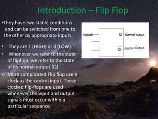
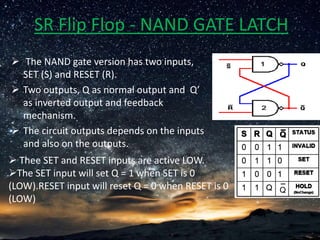
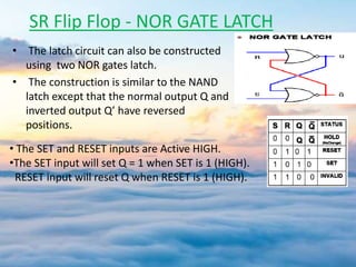
The document presents a detailed overview of flip-flops, which are bi-stable multivibrators used in digital circuits to store binary data (0 or 1). It outlines various types of flip-flops including SR, JK, and D flip-flops, and explains their functionalities, construction using NAND or NOR gates, and behaviors in relation to clock signals. The presentation emphasizes their applications in memory circuits, logic control devices, and counters.


![SEQUENTIAL CIRCUITS [Flip-flops and Latches]](https://cdn.slidesharecdn.com/ss_thumbnails/sequentialcircuits-211217082412-thumbnail.jpg?width=640&height=640&fit=bounds)


![SEQUENTIAL CIRCUITS [FLIP FLOPS AND LATCHES]](https://cdn.slidesharecdn.com/ss_thumbnails/sequentialcircuits-211203044039-thumbnail.jpg?width=640&height=640&fit=bounds)


![16148_flip-flopaaaaaaaaaaaaaaaaa1[1].ppt](https://cdn.slidesharecdn.com/ss_thumbnails/16148flip-flop11-241007142703-8f186e77-thumbnail.jpg?width=640&height=640&fit=bounds)