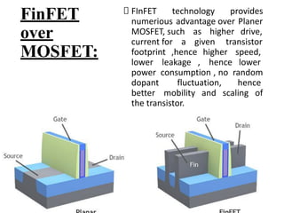
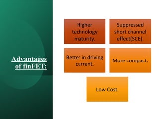
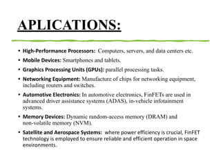
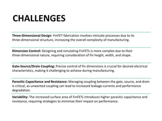
Contents :
Why FinFET?
FinFET over MOSFET
Introduction to FinFET
Working of a FinFET
About the Fin
Where is FinFET Used
Types of FinFET
Applicatons
Advantages of FinFET
Disadvantages of FinFET
Concluison
Why FinFET?
Ø Moore's Law Extension: They play a pivotal role in
extending Moore's Law by enabling
ongoing advancements in chip technology.
Ø Scaling: Scaling down the size below 100nm
increased Ioff
increasing the power consumption of chip
Ø Many solution have been adapted to reduce the
current leakage problem. eg. Changing material of
gate, gate oxide, adding extra layer of buried insulator etc.
Ø 3D Structure: FinFETs have a 3D design, enhancing
control of channel for the flow of electrical current
through the gate wrapped in 3 directions.
Ø Low Power Consumption: FinFETs offer low leakage
current, ideal for energy-efficient devices.
Ø First tri-gate: Intel's 22nm technology in 2011.
FinFET
over
MOSFET:
FInFET technology provides
numerious advantage over Planer
MOSFET, such as higher drive,
current for a given transistor
footprint ,hence higher speed,
lower leakage , hence lower
power consumption , no random
dopant fluctuation, hence
better mobility and scaling of
the transistor.
Introduction:
Ø FinFET is a multi-gate Metal
Oxide Semiconductor Field
Effect Transistor (MOSFET)."
Ø Developed at the University of
Berkeley, California, by
Chenming Hu and colleagues.
Ø Multi-gate transistors integrate
more than one gate into a
single transistor.
Working of a FinFET
As opposite to a traditional
planner transistor, the finFET
has an elevated channel or 'fin',
which the gate wraps around.
Due to the structure, finFET
generate much lower leakage
power and allow greater
devices density.
Compared to planner transistor,
finFET operate at a lower
voltage and offer higher driver
current.
About the Fin:
FinFETs have a vertical channel (FIN),
as opposed to the horizontal channel in
planar MOSFETs.
The channel width of a FinFET is
defined in terms of the FIN height,
leading to width quantization.
Increasing the number of fins on a
FinFET structure can enhance the
control of the channel charge,
improving performance.
The fin height is a critical parameter
that determines the stability of the
FinFET structure, with smaller fin
heights resulting in more flexible
structures and longer fin heights
providing greater stability.
Where is
finFET used?
FinFET technology is
being used in many areas
of IC technology where the
3D fins provide added
density for same feature
size.
FinFET technology has
recently seen a major
increase in adoption for
use within integrated
circuits.
Types Of FinFET:
Shorted-Gate
FinFET (SG
FinFET)
Independent-G
ate FinFET (IG
FinFET).
1.Shorted-Gate FinFET (SG Fin
FET):
In SG FinFETs, the front gate and
back gate are physically
connected (shorted).
SG 3 terminal device (S,D,G(G1,G2))
SG FinFETs have both gates working
together to control
channel electrostatics.
SG FinFETs tend to exhibit higher ION
(ON current) and IOFF (OFF current)
compared to IG FinFETs.
Rich design space (Consumes lesser
area)
2.Independent-Gate FinFET (IG
FinFET)
IG-FinFETs are 4-terminal devices.
IG FinFETs, in contrast, have
separate, independent front and back gates.
Both gates are physically isolated, allowing for
different voltages on each gate.
This isolation provides flexibility and the
ability to modulate the Vth by varying
the voltage of G1,G2.
IG-FinFETs have the drawback of requiring
more space area due to the presence of two
separate gate terminals.
Handles better SCE.
Double Gate and Tri Gate:
• Electrically connected as single gate electrode is folded over three
side of the fin.
-2 effective gate –Front & back -Structure almost same as DG
due to thick dielectric layer on FINFET but no hard mask –3
of the fin called Hard Mask effective gates.
-Hard Mask inhibits the electric -Gate controls channel
from field three sides (no
inhibits of electric felds)
Silicon-On-Insulator(SOI)
and Bulk:
Bulk: Fin etches deeper into the substrate.
-Isolation may be STI but
planarization technique
cannot be used.
SOI : fin is defined on the top of a thin layer
of buried oxide – gives dopant free channel.
Box layer reduces leakage – ultralow power
of operation
Fabrication is easier but the substrate is
costlier
Fin width and other dimension of the
transistor can be controlled betterin SOI but
there may be some self heating effects.
Advantages
of finFET:
Higher
technology
maturity.
Suppressed
short channel
effect(SCE).
Better in driving
current.
More compact.
Low Cost.
APLICATIONS:
• High-Performance Processors: Computers, servers, and data centers etc.
• Mobile Devices: Smartphones and tablets.
• Graphics Processing Units (GPUs): parallel processing tasks.
• Networking Equipment: Manufacture of chips for networking equipment,
including routers and switches.
• Automotive Electronics: In automotive electronics, FinFETs are used in
advanced driver assistance systems (ADAS), in-vehicle infotainment
systems.
• Memory Devices: Dynamic random-access memory (DRAM) and
non-volatile memory (NVM).
• Satellite and Aerospace Systems: where power efficiency is crucial, FinFET
technology is employed to ensure reliable and efficient operation in space
environments.
CHALLENGES
Three-Dimensional Design: FinFET fabrication involves intricate processes due to its
three-dimensional structure, increasing the overall complexity of manufacturing.
Dimension Control: Designing and simulating FinFETs is more complex due to their
three-dimensional nature, requiring consideration of fin height, width, and shape.
Gate-Source/Drain Coupling: Precise control of fin dimensions is crucial for desired electrical
characteristics, making it challenging to achieve during manufacturing.
Parasitic Capacitance and Resistance: Managing coupling between the gate, source, and drain
is critical, as unwanted coupling can lead to increased leakage currents and performance
degradation.
Variability: The increased surface area of FinFETs introduces higher parasitic capacitance and
resistance, requiring strategies to minimize their impact on performance.
Conclusion:
In conclusion, FinFETs
represent a significant
advancement in
semiconductor technology.
Their vertical channel
structure, width quantization,
and enhanced gate control
have made them a crucial
component of modern
integrated circuits.
The adoption of FinFETs has
led to smaller, faster, and
more energy-efficient
electronic devices.
This innovation continues to
shape the semiconductor
industry and drive progress in
electronics.
THANKYOU

Presentation finfet - SAGAR GURUNG.pptx.pdf

  • 2.
    Contents : Why FinFET? FinFETover MOSFET Introduction to FinFET Working of a FinFET About the Fin Where is FinFET Used Types of FinFET Applicatons Advantages of FinFET Disadvantages of FinFET Concluison
  • 3.
    Why FinFET? Ø Moore'sLaw Extension: They play a pivotal role in extending Moore's Law by enabling ongoing advancements in chip technology. Ø Scaling: Scaling down the size below 100nm increased Ioff increasing the power consumption of chip Ø Many solution have been adapted to reduce the current leakage problem. eg. Changing material of gate, gate oxide, adding extra layer of buried insulator etc. Ø 3D Structure: FinFETs have a 3D design, enhancing control of channel for the flow of electrical current through the gate wrapped in 3 directions. Ø Low Power Consumption: FinFETs offer low leakage current, ideal for energy-efficient devices. Ø First tri-gate: Intel's 22nm technology in 2011.
  • 5.
    FinFET over MOSFET: FInFET technology provides numeriousadvantage over Planer MOSFET, such as higher drive, current for a given transistor footprint ,hence higher speed, lower leakage , hence lower power consumption , no random dopant fluctuation, hence better mobility and scaling of the transistor.
  • 6.
    Introduction: Ø FinFET isa multi-gate Metal Oxide Semiconductor Field Effect Transistor (MOSFET)." Ø Developed at the University of Berkeley, California, by Chenming Hu and colleagues. Ø Multi-gate transistors integrate more than one gate into a single transistor.
  • 7.
    Working of aFinFET As opposite to a traditional planner transistor, the finFET has an elevated channel or 'fin', which the gate wraps around. Due to the structure, finFET generate much lower leakage power and allow greater devices density. Compared to planner transistor, finFET operate at a lower voltage and offer higher driver current.
  • 8.
    About the Fin: FinFETshave a vertical channel (FIN), as opposed to the horizontal channel in planar MOSFETs. The channel width of a FinFET is defined in terms of the FIN height, leading to width quantization. Increasing the number of fins on a FinFET structure can enhance the control of the channel charge, improving performance. The fin height is a critical parameter that determines the stability of the FinFET structure, with smaller fin heights resulting in more flexible structures and longer fin heights providing greater stability.
  • 9.
    Where is finFET used? FinFETtechnology is being used in many areas of IC technology where the 3D fins provide added density for same feature size. FinFET technology has recently seen a major increase in adoption for use within integrated circuits.
  • 10.
    Types Of FinFET: Shorted-Gate FinFET(SG FinFET) Independent-G ate FinFET (IG FinFET).
  • 11.
    1.Shorted-Gate FinFET (SGFin FET): In SG FinFETs, the front gate and back gate are physically connected (shorted). SG 3 terminal device (S,D,G(G1,G2)) SG FinFETs have both gates working together to control channel electrostatics. SG FinFETs tend to exhibit higher ION (ON current) and IOFF (OFF current) compared to IG FinFETs. Rich design space (Consumes lesser area)
  • 12.
    2.Independent-Gate FinFET (IG FinFET) IG-FinFETsare 4-terminal devices. IG FinFETs, in contrast, have separate, independent front and back gates. Both gates are physically isolated, allowing for different voltages on each gate. This isolation provides flexibility and the ability to modulate the Vth by varying the voltage of G1,G2. IG-FinFETs have the drawback of requiring more space area due to the presence of two separate gate terminals. Handles better SCE.
  • 13.
    Double Gate andTri Gate: • Electrically connected as single gate electrode is folded over three side of the fin. -2 effective gate –Front & back -Structure almost same as DG due to thick dielectric layer on FINFET but no hard mask –3 of the fin called Hard Mask effective gates. -Hard Mask inhibits the electric -Gate controls channel from field three sides (no inhibits of electric felds)
  • 14.
    Silicon-On-Insulator(SOI) and Bulk: Bulk: Finetches deeper into the substrate. -Isolation may be STI but planarization technique cannot be used. SOI : fin is defined on the top of a thin layer of buried oxide – gives dopant free channel. Box layer reduces leakage – ultralow power of operation Fabrication is easier but the substrate is costlier Fin width and other dimension of the transistor can be controlled betterin SOI but there may be some self heating effects.
  • 15.
  • 16.
    APLICATIONS: • High-Performance Processors:Computers, servers, and data centers etc. • Mobile Devices: Smartphones and tablets. • Graphics Processing Units (GPUs): parallel processing tasks. • Networking Equipment: Manufacture of chips for networking equipment, including routers and switches. • Automotive Electronics: In automotive electronics, FinFETs are used in advanced driver assistance systems (ADAS), in-vehicle infotainment systems. • Memory Devices: Dynamic random-access memory (DRAM) and non-volatile memory (NVM). • Satellite and Aerospace Systems: where power efficiency is crucial, FinFET technology is employed to ensure reliable and efficient operation in space environments.
  • 17.
    CHALLENGES Three-Dimensional Design: FinFETfabrication involves intricate processes due to its three-dimensional structure, increasing the overall complexity of manufacturing. Dimension Control: Designing and simulating FinFETs is more complex due to their three-dimensional nature, requiring consideration of fin height, width, and shape. Gate-Source/Drain Coupling: Precise control of fin dimensions is crucial for desired electrical characteristics, making it challenging to achieve during manufacturing. Parasitic Capacitance and Resistance: Managing coupling between the gate, source, and drain is critical, as unwanted coupling can lead to increased leakage currents and performance degradation. Variability: The increased surface area of FinFETs introduces higher parasitic capacitance and resistance, requiring strategies to minimize their impact on performance.
  • 18.
    Conclusion: In conclusion, FinFETs representa significant advancement in semiconductor technology. Their vertical channel structure, width quantization, and enhanced gate control have made them a crucial component of modern integrated circuits. The adoption of FinFETs has led to smaller, faster, and more energy-efficient electronic devices. This innovation continues to shape the semiconductor industry and drive progress in electronics.
  • 19.