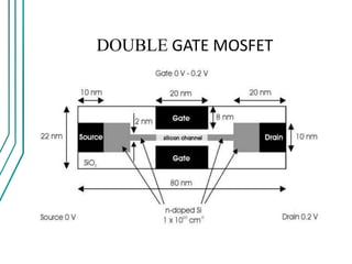
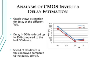
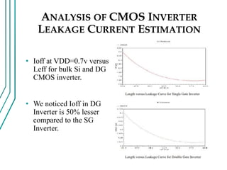
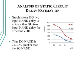
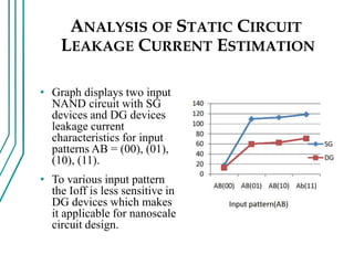
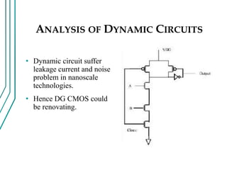
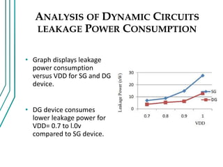
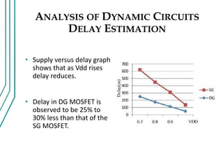
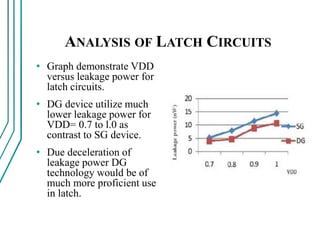
OBJECTIVE
• Compared to Single gate MOSFET Leakage
Current & Delay are to be reduced in Double Gate
MOSFET.
• Short Channel characteristics also improved.
• Double gate MOSFET -low power & high
performance application.
INTRODUCTION
• CMOS technology is the dominant semiconductor
technology for ASIC, microprocessors and
memories
• The constant scaling of CMOS technology
decreases of MOSFET dimensions
• Device performance reduced in terms of the short
channel effect and the leakage current in single
gate MOSFET
DOUBLE GATE MOSFET
IDEA BEHIND DOUBLE GATE
MOSFET
• The main idea of a Double Gate MOSFET is to
control the Si channel very efficiently by choosing
the Si channel width to be very small and by
applying a gate contact to both sides of the
channel.
• This concept helps to suppress short channel
effects and leads to higher currents as compared
with a MOSFET having only one gate
NEED FOR DG MOSFET
• Double gate is comprised of conducting channel
which is usually undoped and surrounded by gate
electrodes on their sides just to ensure that no part
of channel is far away from a gate electrode.
• The voltage applied on the gate terminal control
the electric field determining the amount of
current flow through the channel.
STRUCTURE OF A DG MOSFET
DG MOSFET CONCEPT
• DG MOSFET introduces the concept of Volume
Inversion.
• The inversion charge spreads throughout the SI-
body, which improves the device characteristics.
DG MOSFET STRUCTURE
• Due to its intrinsic strength to short channel
effects and it improves the current driving
capability
• The DG MOSFET has been the focus of much
attention for the application of RF switch
OPERATION OF DG MOSFET
• In the DG mosfet, when voltage is applied to the
gate device, the active silicon region is so thick,
that the control region of the silicon remains
controlled by the majority carriers in the region.
• This causes two different channels. These
channels are separated by enough distance as to be
independent of each other.
EFFECTS OF DG MOSFET ON
LEAKAGE CURRENT
• Reduces SCE effect
• Reduces Sub-threshold Leakage Current
• DG devices requires low electrical field
EFFECTS OF DG MOSFET ON
POWER CIRCUITS
• Independent control of both gates can be use dto
improve the performance and to reduce the power
loss in the circuits.
• Independent DG can be applied to implement
universal logic functionality within a single
transistor.
DESIGN OF DOUBLE GATE
MOSFET
• For low power circuits,
the double gate
technology is most
suitable as the front gate
and back gate are
electrically coupled thus
reducing standby power.
• Using Cadence Virtuoso
tool at 45nm technology
we design & analysis
symmetrical double gate
n-FET with Leff=45nm,
toxf=toxb=2.2nm,tsi=8n.
ANALYSIS OF CMOS INVERTER
DELAY ESTIMATION
• Graph shows estimation
for delay at the different
Vdd.
• Delay in DG is reduced up
to 25% compared to the
bulk SG device.
• Speed of DG device is
thus improved compared
to the bulk Si device.
ANALYSIS OF CMOS INVERTER
LEAKAGE CURRENT ESTIMATION
• Ioff at VDD=0.7v versus
Leff for bulk Si and DG
CMOS inverter.
• We noticed Ioff in DG
Inverter is 50% lesser
compared to the SG
Inverter.
ANALYSIS OF STATIC CIRCUIT
DELAY ESTIMATION
• Graph shows DG two
input NAND delay is
inferior than SG two
input NAND delay for
different VDD.
• Thus DG NAND is
25-30% quicker than
the SG NAND.
ANALYSIS OF STATIC CIRCUIT
LEAKAGE CURRENT ESTIMATION
• Graph displays two input
NAND circuit with SG
devices and DG devices
leakage current
characteristics for input
patterns AB = (00), (01),
(10), (11).
• To various input pattern
the Ioff is less sensitive in
DG devices which makes
it applicable for nanoscale
circuit design.
ANALYSIS OF DYNAMIC CIRCUITS
• Dynamic circuit suffer
leakage current and noise
problem in nanoscale
technologies.
• Hence DG CMOS could
be renovating.
ANALYSIS OF DYNAMIC CIRCUITS
LEAKAGE POWER CONSUMPTION
• Graph displays leakage
power consumption
versus VDD for SG and DG
device.
• DG device consumes
lower leakage power for
VDD= 0.7 to l.0v
compared to SG device.
ANALYSIS OF DYNAMIC CIRCUITS
DELAY ESTIMATION
• Supply versus delay graph
shows that as Vdd rises
delay reduces.
• Delay in DG MOSFET is
observed to be 25% to
30% less than that of the
SG MOSFET.
CONCLUSION
• In concluding scaled technology, CMOS circuit leakage
current would be significantly lowered by DG circuits.
• Circuit power and performance presented at 45nm shows
DG inverter could propose 40% lower leakages current,
25% faster performance.
• Compared with bulk Si counterpart technology, it is also
considered that 45nm DG CMOS technology would
support much lower leakage power for dynamic circuit and
latches.
• Here we concluded that DG is in supreme state which
would craft sub-nanoscale CMOS circuit design further
elastic.
ANALYSIS OF LATCH CIRCUITS
• Graph demonstrate VDD
versus leakage power for
latch circuits.
• DG device utilize much
lower leakage power for
VDD= 0.7 to l.0 as
contrast to SG device.
• Due deceleration of
leakage power DG
technology would be of
much more proficient use
in latch.
ICIECA 2014 Paper 23

ICIECA 2014 Paper 23

  • 2.
    OBJECTIVE • Compared toSingle gate MOSFET Leakage Current & Delay are to be reduced in Double Gate MOSFET. • Short Channel characteristics also improved. • Double gate MOSFET -low power & high performance application.
  • 3.
    INTRODUCTION • CMOS technologyis the dominant semiconductor technology for ASIC, microprocessors and memories • The constant scaling of CMOS technology decreases of MOSFET dimensions • Device performance reduced in terms of the short channel effect and the leakage current in single gate MOSFET
  • 4.
  • 5.
    IDEA BEHIND DOUBLEGATE MOSFET • The main idea of a Double Gate MOSFET is to control the Si channel very efficiently by choosing the Si channel width to be very small and by applying a gate contact to both sides of the channel. • This concept helps to suppress short channel effects and leads to higher currents as compared with a MOSFET having only one gate
  • 6.
    NEED FOR DGMOSFET • Double gate is comprised of conducting channel which is usually undoped and surrounded by gate electrodes on their sides just to ensure that no part of channel is far away from a gate electrode. • The voltage applied on the gate terminal control the electric field determining the amount of current flow through the channel.
  • 7.
    STRUCTURE OF ADG MOSFET
  • 8.
    DG MOSFET CONCEPT •DG MOSFET introduces the concept of Volume Inversion. • The inversion charge spreads throughout the SI- body, which improves the device characteristics.
  • 9.
    DG MOSFET STRUCTURE •Due to its intrinsic strength to short channel effects and it improves the current driving capability • The DG MOSFET has been the focus of much attention for the application of RF switch
  • 10.
    OPERATION OF DGMOSFET • In the DG mosfet, when voltage is applied to the gate device, the active silicon region is so thick, that the control region of the silicon remains controlled by the majority carriers in the region. • This causes two different channels. These channels are separated by enough distance as to be independent of each other.
  • 11.
    EFFECTS OF DGMOSFET ON LEAKAGE CURRENT • Reduces SCE effect • Reduces Sub-threshold Leakage Current • DG devices requires low electrical field
  • 12.
    EFFECTS OF DGMOSFET ON POWER CIRCUITS • Independent control of both gates can be use dto improve the performance and to reduce the power loss in the circuits. • Independent DG can be applied to implement universal logic functionality within a single transistor.
  • 13.
    DESIGN OF DOUBLEGATE MOSFET • For low power circuits, the double gate technology is most suitable as the front gate and back gate are electrically coupled thus reducing standby power. • Using Cadence Virtuoso tool at 45nm technology we design & analysis symmetrical double gate n-FET with Leff=45nm, toxf=toxb=2.2nm,tsi=8n.
  • 14.
    ANALYSIS OF CMOSINVERTER DELAY ESTIMATION • Graph shows estimation for delay at the different Vdd. • Delay in DG is reduced up to 25% compared to the bulk SG device. • Speed of DG device is thus improved compared to the bulk Si device.
  • 15.
    ANALYSIS OF CMOSINVERTER LEAKAGE CURRENT ESTIMATION • Ioff at VDD=0.7v versus Leff for bulk Si and DG CMOS inverter. • We noticed Ioff in DG Inverter is 50% lesser compared to the SG Inverter.
  • 16.
    ANALYSIS OF STATICCIRCUIT DELAY ESTIMATION • Graph shows DG two input NAND delay is inferior than SG two input NAND delay for different VDD. • Thus DG NAND is 25-30% quicker than the SG NAND.
  • 17.
    ANALYSIS OF STATICCIRCUIT LEAKAGE CURRENT ESTIMATION • Graph displays two input NAND circuit with SG devices and DG devices leakage current characteristics for input patterns AB = (00), (01), (10), (11). • To various input pattern the Ioff is less sensitive in DG devices which makes it applicable for nanoscale circuit design.
  • 18.
    ANALYSIS OF DYNAMICCIRCUITS • Dynamic circuit suffer leakage current and noise problem in nanoscale technologies. • Hence DG CMOS could be renovating.
  • 19.
    ANALYSIS OF DYNAMICCIRCUITS LEAKAGE POWER CONSUMPTION • Graph displays leakage power consumption versus VDD for SG and DG device. • DG device consumes lower leakage power for VDD= 0.7 to l.0v compared to SG device.
  • 20.
    ANALYSIS OF DYNAMICCIRCUITS DELAY ESTIMATION • Supply versus delay graph shows that as Vdd rises delay reduces. • Delay in DG MOSFET is observed to be 25% to 30% less than that of the SG MOSFET.
  • 21.
    CONCLUSION • In concludingscaled technology, CMOS circuit leakage current would be significantly lowered by DG circuits. • Circuit power and performance presented at 45nm shows DG inverter could propose 40% lower leakages current, 25% faster performance. • Compared with bulk Si counterpart technology, it is also considered that 45nm DG CMOS technology would support much lower leakage power for dynamic circuit and latches. • Here we concluded that DG is in supreme state which would craft sub-nanoscale CMOS circuit design further elastic.
  • 22.
    ANALYSIS OF LATCHCIRCUITS • Graph demonstrate VDD versus leakage power for latch circuits. • DG device utilize much lower leakage power for VDD= 0.7 to l.0 as contrast to SG device. • Due deceleration of leakage power DG technology would be of much more proficient use in latch.