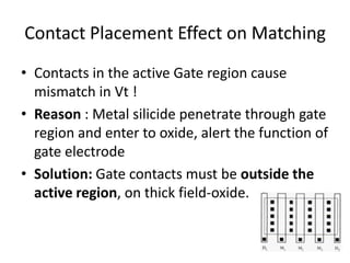
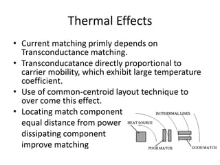
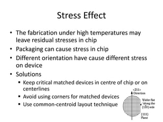
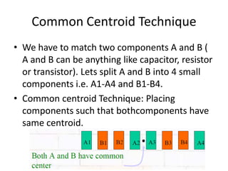
Download as PDF, PPTX

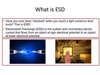
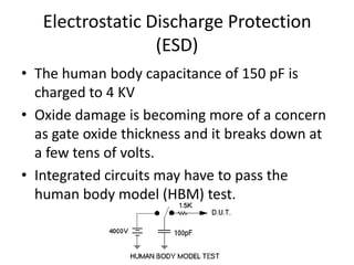
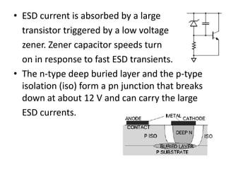


The document discusses techniques for achieving device matching in microelectronics, focusing on MOS transistors. It outlines methods to minimize voltage and current mismatches, factors affecting transistor matching such as device size, orientation, and thermal effects, and introduces the common centroid layout technique for effective matching. Additionally, it briefly covers electrostatic discharge (ESD) protection measures relevant to integrated circuits.


