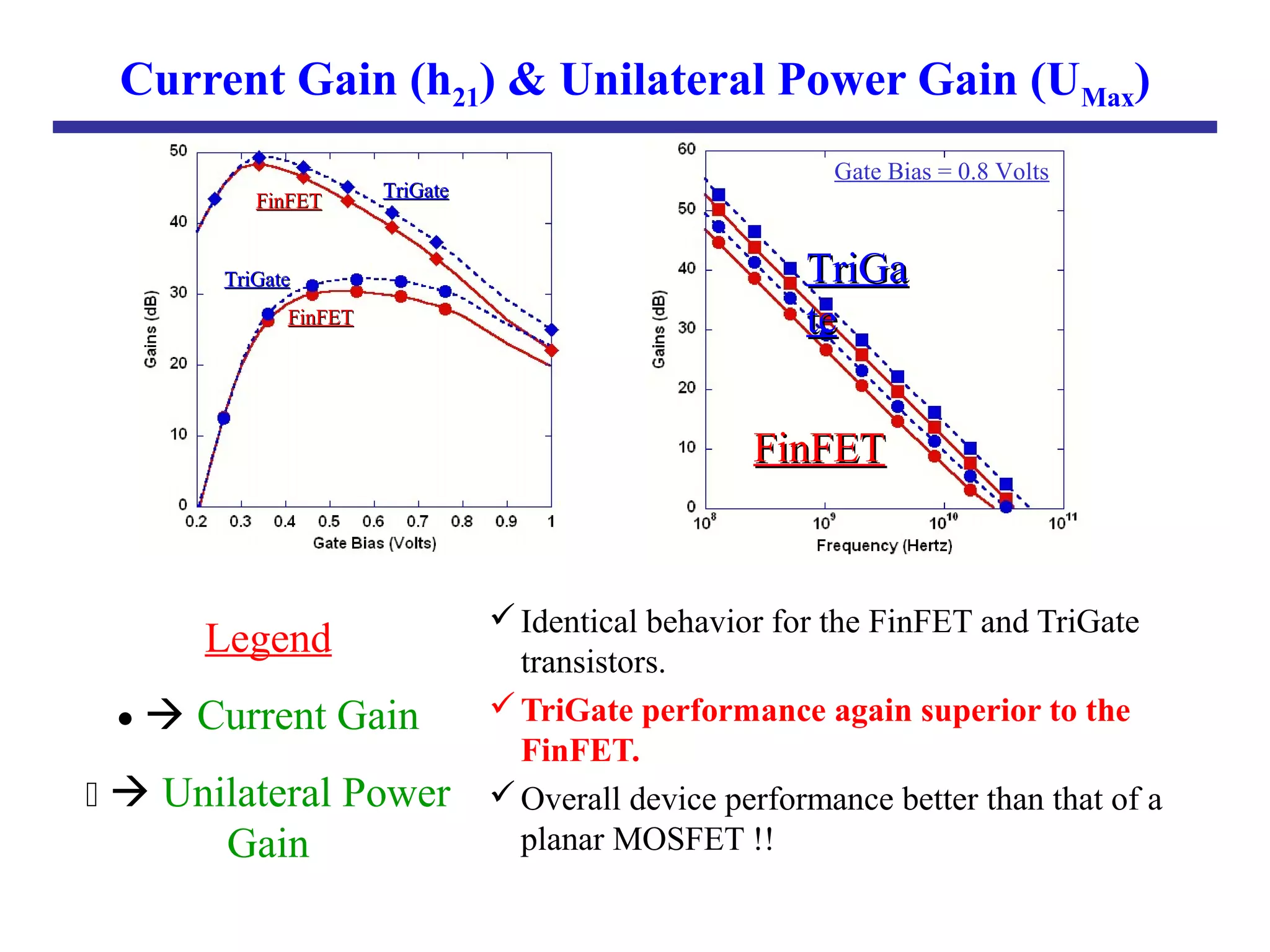
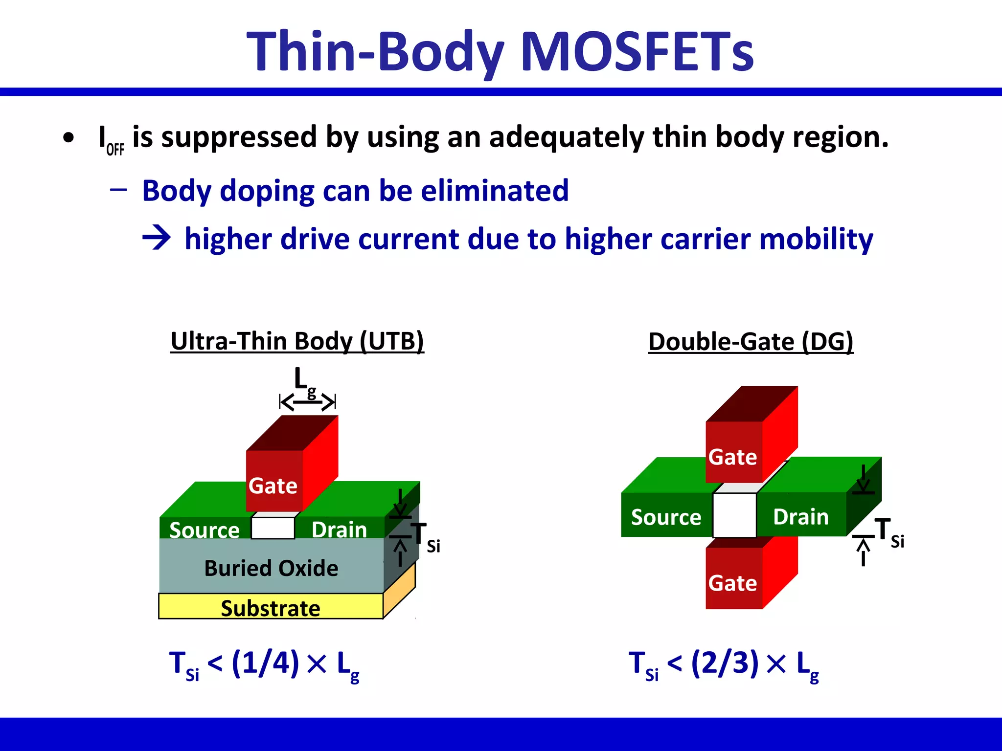
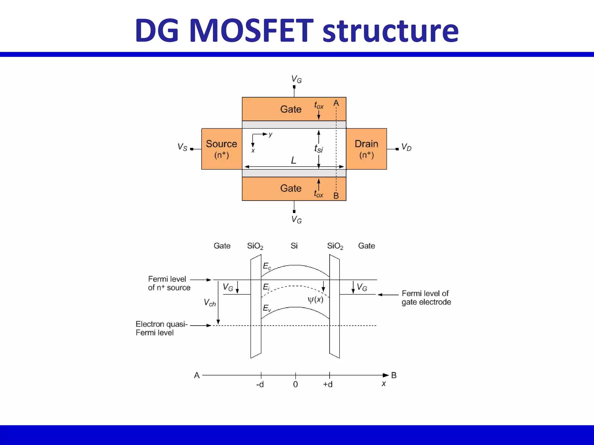
NANO-SCALE DOUBLE-GATE
MOSFETS IN LOW POWER
TUNABLE CURRENT MODE
Presented by
RM.Naatchammai,V.P.M.M.Engineering College
C.Rajalakshmi ,V.P.M.M.Engineering College
ROUTE MAP
Source Tunable current mirrors
Tunable current amplifiers
Current-mode integrator
Destination
A Vision of the Future
3
SOI – The technology of the future.
Highlights
• Reduced junction capacitance.
• Absence of latchup.
• Ease in scaling (buried oxide need not
be scaled).
• Compatible with conventional Silicon
processing.
• Sometimes requires fewer steps to
fabricate.
• Reduced leakage.
• Improvement in the soft error rate.
Welcome to the world of Silicon On Insulator
Drawbacks
• Drain Current Overshoot.
• Kink effect
• Thickness control (fully
depleted operation).
• Surface states.
Why New Transistor Structures?
• Off-state leakage (IOFF) must be suppressed as Lgis scaled down
– allows for reductions in VT and hence VDD
• Leakage occurs in the region away from the channel surface
 Let’s get rid of it!
DrainSource
Gate
Lg
Thin-Body
MOSFET:
Buried Oxide
Source Drain
Gate
Substrate
“Silicon-on-
Insulator” (SOI)
Wafer
Thin-Body MOSFETs
• IOFF is suppressed by using an adequately thin body region.
– Body doping can be eliminated
 higher drive current due to higher carrier mobility
Ultra-Thin Body (UTB)
Buried Oxide
Substrate
Source Drain
Gate
TSi
Lg
TSi < (1/4) × Lg
Double-Gate (DG)
Gate
Source Drain
Gate
TSi
TSi < (2/3) × Lg
DG MOSFET structure
Effect of TSi on OFF-state Leakage
IOFF = 19 µA/µmIOFF = 2.1 nA/µm
Leakage Current
Density [A/cm2
]
@ VDS = 0.7 V
106
10-1
3x10²
0.0
4.0
8.0
12.0
16.0
20.0
G
G
S D
G
G
S D
Si Thickness [nm]
Lg = 25 nm; tox,eq = 12Å
TSi = 10 nm TSi = 20 nm
Double-Gate MOSFET Structures
PLANAR:
VERTICAL FINFET:
Double-Gate FinFET
• Self-aligned gates straddle narrow silicon fin
• Current flows parallel to wafer surface
Source
Drain
Gate 2Gate 2
Fin Width Wfin = TSi
Fin Height Hfin = W
Gate Length = Lg
Current
Flow
Gate 1Gate 1
GG
GG
S
D
Concept of Current Mirror
• The motivation behind a current mirror is to
sense the current from a “golden current source”
and duplicate this “golden current” to other
locations.
Bulk FinFET (Samsung Electronics)
• FinFETs can be made
on bulk-Si wafers
lower cost
improved thermal
conduction
• 90 nm Lg FinFETs
demonstrated
• Wfin = 80 nm
• Hfin = 100 nm
DIBL = 25 mV
Current Gain (h21) & Unilateral Power Gain (UMax)
Identical behavior for the FinFET and TriGate
transistors.
TriGate performance again superior to the
FinFET.
Overall device performance better than that of a
planar MOSFET !!
Legend
•  Current Gain
  Unilateral Power
Gain
Gate Bias = 0.8 Volts
FinFETFinFET
TriGaTriGa
tete
FinFETFinFET TriGateTriGate
FinFETFinFET
TriGateTriGate
CMOS Current Mirror
• The idea of combining NMOS and PMOS to
produce CMOS current mirror is shown above.
Tunable current amplifier
One Further Improvement current mirror circuit
we get current mirror amplifier
Simulation results
performed with
the AMS software 4.0.2.1 from Mentor Graphics
IDS(VGS) at VDS = 0.25, 0.5, 0.75, 1V
IDS
VGS
16
IBMs FinFET / Double-Gate SOI (Nanoscale Device Research
Group)
Device Structural Variations (Channel Doping)
• Near identical behavior in both graphs.
• Channel doping normally maintained at a low value to
minimize effects of scattering.
• Mobility degradation observed at high values of channel
doping.
• Moderate levels of channel doping could be used.
FinFET
TriGate
Ω-Gate
Quad-Gate
Fin Height/Width = 50 nm
Gate Length = 50 nm
Workfunction = 4.6 eV
Oxide Thickness = 2 nm
Device
Dimensions
A Vision of the Future
Information technology will be
• pervasive
• embedded
• human-centered
Philips Transportation
Health
care Disaster response
Energy
Environment
Sensatex
• solving societal
scale problems
Infrastructural
core
The “Cloud”
The “Swarm”
Mobile Devices
Market Growth
Better Energy Efficiency
& Functionality,
Lower Cost
Diversification of Devices & Materials
Heterogeneous
Integration
Investment
Conclusions and Future Work
Conclusions:
• Successfully modeled devices in 3-dimensions.
• Understood device design space and scaling constraints.
• Undertook a study to understand fabrication tolerances to which
every device could be exposed.
• Both sub-threshold and RF performance explored.
Future Work:
• Model p-channel devices, scaling rules could differ.
• Understand device design in totality given a variation in two or more
than two parameters.
• Investigate their Microwave characteristics.
• Comparison with n-channel performance for CMOS and BiCMOS
incorporation.
• Understand effects of temperature on device performance.
Rm.naatchammai vlsi paper ppt

Rm.naatchammai vlsi paper ppt

  • 1.
    NANO-SCALE DOUBLE-GATE MOSFETS INLOW POWER TUNABLE CURRENT MODE Presented by RM.Naatchammai,V.P.M.M.Engineering College C.Rajalakshmi ,V.P.M.M.Engineering College
  • 2.
    ROUTE MAP Source Tunablecurrent mirrors Tunable current amplifiers Current-mode integrator Destination A Vision of the Future
  • 3.
    3 SOI – Thetechnology of the future. Highlights • Reduced junction capacitance. • Absence of latchup. • Ease in scaling (buried oxide need not be scaled). • Compatible with conventional Silicon processing. • Sometimes requires fewer steps to fabricate. • Reduced leakage. • Improvement in the soft error rate. Welcome to the world of Silicon On Insulator Drawbacks • Drain Current Overshoot. • Kink effect • Thickness control (fully depleted operation). • Surface states.
  • 4.
    Why New TransistorStructures? • Off-state leakage (IOFF) must be suppressed as Lgis scaled down – allows for reductions in VT and hence VDD • Leakage occurs in the region away from the channel surface  Let’s get rid of it! DrainSource Gate Lg Thin-Body MOSFET: Buried Oxide Source Drain Gate Substrate “Silicon-on- Insulator” (SOI) Wafer
  • 5.
    Thin-Body MOSFETs • IOFFis suppressed by using an adequately thin body region. – Body doping can be eliminated  higher drive current due to higher carrier mobility Ultra-Thin Body (UTB) Buried Oxide Substrate Source Drain Gate TSi Lg TSi < (1/4) × Lg Double-Gate (DG) Gate Source Drain Gate TSi TSi < (2/3) × Lg
  • 6.
  • 7.
    Effect of TSion OFF-state Leakage IOFF = 19 µA/µmIOFF = 2.1 nA/µm Leakage Current Density [A/cm2 ] @ VDS = 0.7 V 106 10-1 3x10² 0.0 4.0 8.0 12.0 16.0 20.0 G G S D G G S D Si Thickness [nm] Lg = 25 nm; tox,eq = 12Å TSi = 10 nm TSi = 20 nm
  • 8.
  • 9.
    Double-Gate FinFET • Self-alignedgates straddle narrow silicon fin • Current flows parallel to wafer surface Source Drain Gate 2Gate 2 Fin Width Wfin = TSi Fin Height Hfin = W Gate Length = Lg Current Flow Gate 1Gate 1 GG GG S D
  • 10.
    Concept of CurrentMirror • The motivation behind a current mirror is to sense the current from a “golden current source” and duplicate this “golden current” to other locations.
  • 11.
    Bulk FinFET (SamsungElectronics) • FinFETs can be made on bulk-Si wafers lower cost improved thermal conduction • 90 nm Lg FinFETs demonstrated • Wfin = 80 nm • Hfin = 100 nm DIBL = 25 mV
  • 12.
    Current Gain (h21)& Unilateral Power Gain (UMax) Identical behavior for the FinFET and TriGate transistors. TriGate performance again superior to the FinFET. Overall device performance better than that of a planar MOSFET !! Legend •  Current Gain   Unilateral Power Gain Gate Bias = 0.8 Volts FinFETFinFET TriGaTriGa tete FinFETFinFET TriGateTriGate FinFETFinFET TriGateTriGate
  • 13.
    CMOS Current Mirror •The idea of combining NMOS and PMOS to produce CMOS current mirror is shown above.
  • 14.
    Tunable current amplifier OneFurther Improvement current mirror circuit we get current mirror amplifier
  • 15.
    Simulation results performed with theAMS software 4.0.2.1 from Mentor Graphics IDS(VGS) at VDS = 0.25, 0.5, 0.75, 1V IDS VGS
  • 16.
    16 IBMs FinFET /Double-Gate SOI (Nanoscale Device Research Group)
  • 17.
    Device Structural Variations(Channel Doping) • Near identical behavior in both graphs. • Channel doping normally maintained at a low value to minimize effects of scattering. • Mobility degradation observed at high values of channel doping. • Moderate levels of channel doping could be used. FinFET TriGate Ω-Gate Quad-Gate Fin Height/Width = 50 nm Gate Length = 50 nm Workfunction = 4.6 eV Oxide Thickness = 2 nm Device Dimensions
  • 18.
    A Vision ofthe Future Information technology will be • pervasive • embedded • human-centered Philips Transportation Health care Disaster response Energy Environment Sensatex • solving societal scale problems Infrastructural core The “Cloud” The “Swarm” Mobile Devices Market Growth Better Energy Efficiency & Functionality, Lower Cost Diversification of Devices & Materials Heterogeneous Integration Investment
  • 19.
    Conclusions and FutureWork Conclusions: • Successfully modeled devices in 3-dimensions. • Understood device design space and scaling constraints. • Undertook a study to understand fabrication tolerances to which every device could be exposed. • Both sub-threshold and RF performance explored. Future Work: • Model p-channel devices, scaling rules could differ. • Understand device design in totality given a variation in two or more than two parameters. • Investigate their Microwave characteristics. • Comparison with n-channel performance for CMOS and BiCMOS incorporation. • Understand effects of temperature on device performance.