Downloaded 25 times
![Ankita Wagadre Int. Journal of Engineering Research and Applications www.ijera.com
ISSN : 2248-9622, Vol. 4, Issue 7( Version 1), July 2014, pp.30-34
www.ijera.com 30 | P a g e
Design & Performance Analysis of DG-MOSFET for Reduction of Short Channel Effect over Bulk MOSFET at 20nm Ankita Wagadre*, Shashank Mane** *(Research scholar, Department of Electronics & Communication, SBITM, Betul-460001) ** (Assistant Professor, Department of Electronics & Communication, SBITM, Betul-460001) ABSTRACT An aggressive scaling of conventional MOSFETs channel length reduces below 100nm and gate oxide thickness below 3nm to improved performance and packaging density. Due to this scaling short channel effect (SCEs) like threshold voltage, Subthreshold slope, ON current and OFF current plays a major role in determining the performance of scaled devices. The double gate (DG) MOSFETS are electro-statically superior to a single gate (SG) MOSFET and allows for additional gate length scaling. Simulation work on both devices has been carried out and presented in paper. The comparative study had been carried out for threshold voltage (VT), Subthreshold slope (Sub VT), ION and IOFF Current. It is observed that DG MOSFET provide good control on leakage current over conventional Bulk (Single Gate) MOSFET. The VT (Threshold Voltage) is 2.7 times greater than & ION of DG MOSFET is 2.2 times smaller than the conventional Bulk (Single Gate) MOSFET.
Keywords - DG MOSFET (Double Gate Metal oxide Field Effect Transistor), Short Channel Effect (SCE), Bulk (Single Gate) MOSFET.
I. INTRODUCTION
The downscaling of metal-oxide-semiconductor field-effect transistor, MOSFET has been popular for decades ago to get the well circuit performance and to suit Moore‟s law as well as the direction shown by International Technology Roadmap for Semiconductor, ITRS 2012. From last 4 decade, semiconductor device technology has changed with an amazing speed [1]. There is an exponential growth in integrated circuit performance, the scaling of MOSFET dimensions and its structure has been the primary driver. From the vantage point of today, in the 45 nm process era, we look 5 years into the future and find that the double-gate MOSFET (DG- MOSFET) is widely expected to take over for the long-lasting industrial favorite, than the single-gate MOSFET [2]. As scaling is expected to reach the 14 nm era in a few years, the DGMOSFET becomes necessary in terms of its superior properties in this scaling region [3].Current CMOS technology, conventional MOSFET will be difficult to scale further, even if we use high-k gate dielectrics, metal electrodes, strained silicon and other new materials being considered. Multi Gate Field Effect Transistor (MUGFET) is thought to be the leading new transistor technology which will take over as the leading workhorse in digital electronics. International Technology Roadmap for Semiconductor, devices with gate lengths down to 10 nm can be expected in 2019 [3&6].In fact, over the past 3 decades the number of transistors per chip has been doubled every 2–3 years once a new technology node is introduced. For example 45 nm technology node will
have double MOSFETs in a microprocessor than a 65 nm technology node [4]. As MOSFET geometries shrink, the voltage that can be applied to the gate must be reduced to maintain reliability. To reduce the power, the threshold voltage of the MOSFET has to be reduced, but As threshold voltage is decreased, the transistor cannot be switched from complete turn-off to complete turn-on with the limited voltage swing available. Hence sub threshold leakage current is major issue of modern high-performance VLSI chips [5]. A. Double Gate MOSFET Single gate device at nanoscale is suffering from short channel effect that can be overcome by various multi gate structures like Double Gate, trigate & Gate All Around structure. The double gate (DG) MOSFETs are electro-statically superior to a single gate (SG) MOSFET and allows for additional gate length scaling [1]. The DG MOSFETs are the devices, which are having two gates on either side of the channel. One in upper side, known as top gate and another one is in the lower side of the channel, known as bottom gate. It gives better control of the channel by the gate electrodes [8]. This ensures that no part of the channel is far away from a gate electrode. The Double- Gate MOSFET (DGMOSFET) structure minimizes short-channel effects that allows more aggressive device downscaling of device up to 10 nm gate length [2]. There are two structures for modeling gate structure i.e Planar& Non-planar [6].
RESEARCH ARTICLE OPEN ACCESS](https://image.slidesharecdn.com/e047013034-140908235857-phpapp01/75/Design-Performance-Analysis-of-DG-MOSFET-for-Reduction-of-Short-Channel-Effect-over-Bulk-MOSFET-at-20nm-1-2048.jpg)
![Ankita Wagadre Int. Journal of Engineering Research and Applications www.ijera.com
ISSN : 2248-9622, Vol. 4, Issue 7( Version 1), July 2014, pp.30-34
www.ijera.com 31 | P a g e
Fig. 1. Schematics of a DG MOSFET with a
planar structure
The Advantages of using planar structure is
better uniformity of Silicon channel thickness & can
use existing fabrication processes. Disadvantages are
fabrication of back gate and gate dielectric
underneath the Silicon channel is difficult &
accessing bottom gate for device wiring is not easy
(may impact device density).Structure shown in fig.1.
Fig. 2. Schematics of a DG MOSFET with a non-planar
structure.
The advantage of using non- planar structure
(Shown in fig. 2) is the easier formation and access of
both gates (wraparound gate) & increases device
density. Disadvantage are channel thickness defined
by lithography (poorer uniformity) front and back
gates cannot be independently biased& from
conventional fabrication processes [6].
As planar structure is easy to design, the DG
planar structure is used for design & stimulation. The
voltage applied on the gate terminals controls the
electric field and determining the current flowing
through the channel. Fig. 3 shows that there are two
mode of operation (a) to switch both gates
simultaneously (b) to switch only one and apply a
bias to the second gate (this is called (“ground plane”
(GP) or “back-gate” (BG)) [5].
(a) (b)
Fig. 3. General Operation of DG MOSFET
structure
II. DESIGN OF DOUBLE GATE MOSFET
(DG-MOSFET)
For designing the proposed device and its
simulation, ATLAS device simulator tool of Silvaco
TCAD is used.
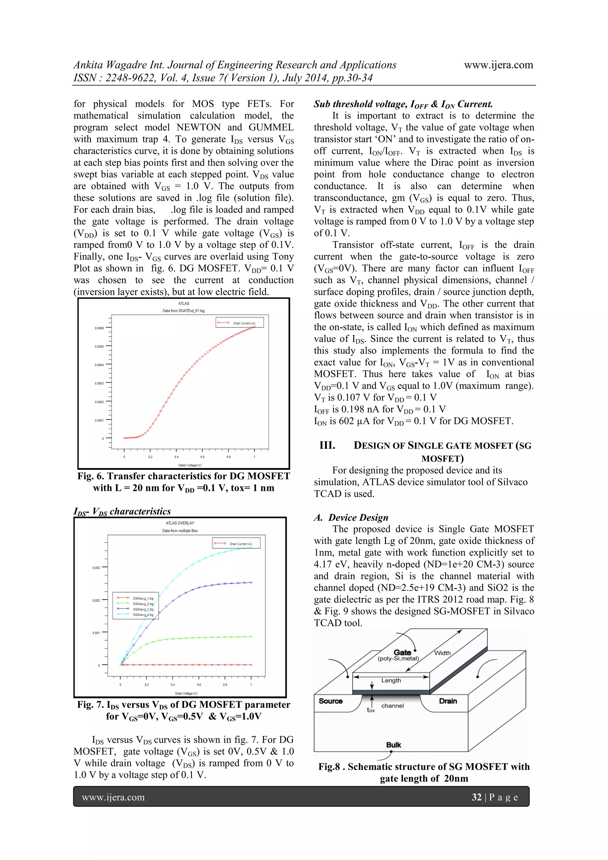
A. Device Design
The proposed device is Double Gate MOSFET
with gate length Lg of 20nm, gate oxide thickness of
1nm, metal gate with work function explicitly set to
4.17 eV, heavily n-doped (ND=1e+21 CM-3) source
and drain region, Si is the channel material with
channel doped (ND=1.5e+19 CM-3) and SiO2 is the
gate dielectric as per the ITRS 2012 road map. Fig.4
& Fig. 5 shows the designed DG-MOSFET in
Silvaco TCAD tool.
Fig. 4. Schematic structure of DG MOSFET with
gate length of 20nm
Fig. 5. Two Dimensional Device Structure of DG
MOSFET
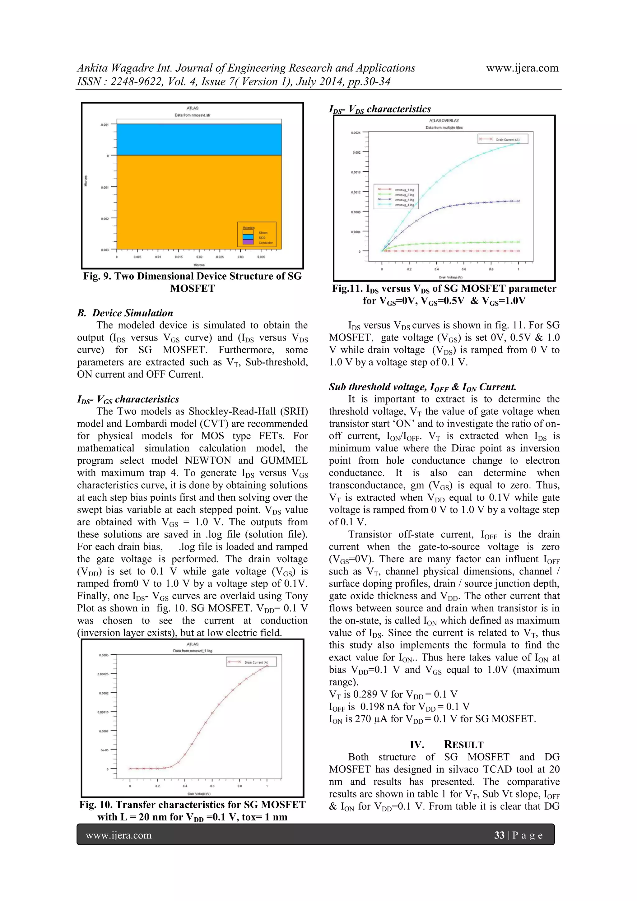
B. Device Simulation
The modeled device is simulated to obtain the
output (IDS versus VGS curve) and (IDS versus VDS
curve) for DG MOSFET. Furthermore, some
parameters are extracted such as VT, Sub-threshold,
ON current and OFF Current.
IDS- VGS characteristics
The Two models as Shockley-Read-Hall (SRH)
model and Lombardi model (CVT) are recommended](https://image.slidesharecdn.com/e047013034-140908235857-phpapp01/75/Design-Performance-Analysis-of-DG-MOSFET-for-Reduction-of-Short-Channel-Effect-over-Bulk-MOSFET-at-20nm-2-2048.jpg)
![Ankita Wagadre Int. Journal of Engineering Research and Applications www.ijera.com
ISSN : 2248-9622, Vol. 4, Issue 7( Version 1), July 2014, pp.30-34
www.ijera.com 34 | P a g e
MOSFET is having good control over current as ION is increased from 270 μA to 602 μA. This will leads to reduction in leakage power in the device & hence to the whole circuit. The VT (Threshold Voltage) is 2.7 times greater than & ION of DG MOSFET 2.2 times smaller than the conventional Bulk (Single Gate) MOSFET.
TABLE I. EXTRACTED DATA OF DG MOSFET & DG CNFET WITH LG=20NM
For VDS = 0.1 V
VT (V)
Sub Vt Slope (mv/dec)
IOFF (nA)
ION (μA)
SG MOSFET
0.289 V
65.5
0.198
270
DG MOSFET
0.107 V
64
158
602
V. CONCLUSION
Short channel effect can be reduced by multigate MOSFETs. Two FET structures have been designed using Silvaco TCAD tool at 20nm technology & comparing the results of Single gate MOSFET & Double Gate MOSFET. Improvement in the device reliability with better reduction of Short Channel Effects has been observed through the simulation results by proper tuning of the channel thickness to ensure the volume inversion. Several structures have been proposed: planar & Non planar. DG MOSFET with planar structure is so far the most promising. Experimental results has presented, the new structure DG MOSFET possesses excellent sub threshold and output characteristics without short-channel effects, demonstrating the shortest gate length. Results shows that leakage current in SG MOSFET is much smaller as compared to that of DG MOSFET, whereas the ON current in DG MOSFET is much larger as compared to that of SG MOSFET. The VT (Threshold Voltage) is 2.7 times greater than & ION of DG MOSFET 2.2 times smaller than the conventional Bulk (Single Gate) MOSFET.
REFERENCES
[1] Mr. Sanjay Chopade & M. Shashank Mane " Design of DG-CNFET For Reduction of Short Channel Effect Over DG MOSFET at 20nm " IEEE Trans., December 2013
[2] Santosh Kumar Gupta et al "Simulation and Analysis of Gate Engineered Triple Metal Double Gate (TM-DG) MOSFET for Diminished Short Channel Effects" IJAST, Vol. 38, January, 2012
[3] A. S. I. Association, “Itrs - international technology roadmap for semiconductor,” 2003.
[4] "1965 – "Moore's Law" Predicts the Future of Integrated Circuits". Computer History Museum.
[5] Kaushik Roy, Kiat Seng Yeo (2004). Low Voltage, Low Power VLSI Subsystems. McGraw-Hill Professional.,p. 4 & 44. ISBN 0-07-143786-X.
[6] Tsu-Jae King Liu"Introduction to Multi-gate MOSFETs" 6th Annual SOI Fundamentals ClassOctober 3, 2012
[7] S. Panigrahy & P. k. Sahu "Analytical Modeling of Double Gate MOSFET and Its Application" IJCSI International Journal of Computer Science Issues, Vol.1,Issue 1,November 2011
[8] Zhihong Chen,et al “Externally Assembled Gate-All-Around Carbon Nanotube Field- Effect Transistor” IEEE electron device letter, Vol. 29, No. 2, 5 February 2008.
[9] Vaidyanathan Subramanian “Multiple Gate Field Effect Transistor for future CMOS” IETE Technical Review, Vol 27, ISSUE-6, NOV-DEC 2010.
[10] Prateek Mishra, Anish Muttreja, and Niraj K. Jha "FinFET Circuit Design"Springer Science+Business Media, LLC 2011
[11] Scott Thompson, Paul Packan, Mark Bohr “MOS Scaling: Transistor Challenges for the 21st Century” Intel Technology Journal Q3‟98
[12] Gaurav Saini, Ashwani K Rana "Physical Scaling Limits of FinFETStructure: A Simulation Study" International Journal of VLSI design & Communication Systems (VLSICS) Vol.2, No.1, March 2011
[13] Wen Wu & Mansun Chan "Analysis of Geometry-Dependent Parasitics in Multifin Double-Gate FinFETs"IEEE Trans. on Electron Devices, Vol.54, No. 4, April 2007](https://image.slidesharecdn.com/e047013034-140908235857-phpapp01/75/Design-Performance-Analysis-of-DG-MOSFET-for-Reduction-of-Short-Channel-Effect-over-Bulk-MOSFET-at-20nm-5-2048.jpg)

The document discusses the design and performance analysis of double gate (DG) MOSFETs in comparison to single gate (SG) MOSFETs, particularly focusing on the reduction of short channel effects at a 20nm technology node. The study reveals that DG MOSFETs demonstrate superior control over leakage current, with significant improvements in threshold voltage and ion current. The findings highlight the potential of DG MOSFETs to enhance device efficiency and meet the challenges posed by aggressive scaling in modern semiconductor technologies.


![MTech Seminar Presentation [IIT-Bombay]](https://cdn.slidesharecdn.com/ss_thumbnails/seminar-presentation-final-140502111554-phpapp02-thumbnail.jpg?width=640&height=640&fit=bounds)