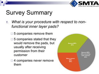
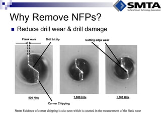
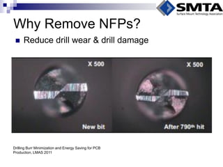
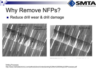
The document discusses the ongoing debate around whether to keep or remove non-functional pads (NFPs) on printed circuit boards. An industry survey found that most suppliers remove unused NFPs to improve drilling and inspection processes. While some believe NFPs help with thermal expansion, most experts recommend their removal, especially for high-speed designs, as they can negatively impact signal integrity. There is limited reliability data but no evidence that removing NFPs causes issues, and it may help prevent problems like drilling damage or shorts. The best approach depends on the specific board design and materials.

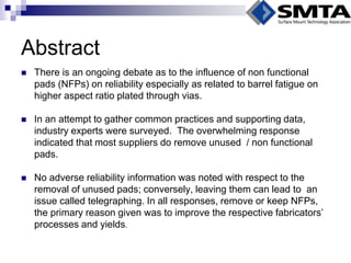
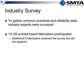


![PTH Reliability for High Aspect Via Holes
NPL reported higher percentage and earlier fails of vias with NFPs
Black Line is NFPs IN
Red Line is NFPs OUT
[2] Wickham Martin, “Through Hole Reliability for High Aspect Via Holes,” NPL Webinar June 11, 2013](https://image.slidesharecdn.com/non-functional-pads-should-they-stay-or-should-they-go-140910085506-phpapp02/85/Non-functional-pads-should-they-stay-or-should-they-go-22-320.jpg)

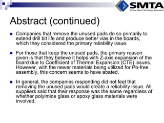
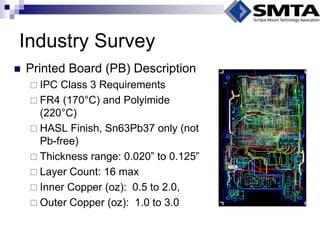
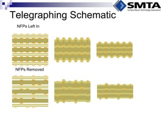
![Reliability Data (continued)
PWB Interconnect reports that “presence of non- functional pads is a determent [sic] to the reliability of PWBs”
Speculated about telegraphing phenomenon: excess copper at PTHs results in resin starvation between pads](https://image.slidesharecdn.com/non-functional-pads-should-they-stay-or-should-they-go-140910085506-phpapp02/85/Non-functional-pads-should-they-stay-or-should-they-go-24-320.jpg)

![References
INDUSTRY REFERENCES
[1] A. Ciccomancini Scogna, “Signal Integrity Analysis of a 26 Layers Board with Emphasis on the Effect of Non-Functional Pads,” IEEE EMC 2008 Symposium.
[2] Wickham Martin, “Through Hole Reliability for High Aspect Via Holes,” NPL Webinar June 11, 2013.
[3] Birch, Bill, “Discussion on Non-functional Pad Removal/Backdrilling and PCB Reliability,” PWB Interconnect Solutions Inc. 103-235 Stafford Road West, Nepean, Ontario, Canada K2H 9C1.
[4] Reid, Paul, “Design and Construction Affects on PWB Reliability,” PWB Interconnect Solutions, IPC APEX EXPO.
[5] Thierauf, Stephen, High-speed Circuit Board Integrity, Artech House, January 2004.
[6] Barker, Donald & Dasgupta, Abhijit, Chapter 20 “Thermal Stress Issues in Plated-Through-Hole Reliability” in Thermal Stress and Strain in Microelectronic Packaging, Van Nostrand Reinhold, 1993.
FABRICATOR REFERENCES
[7] Frank, Bill, “Design for Manufacture,” Multek.
[8] Sanmina, “PCB Fabrication: Opti-Via Technology for Improved Signal Integrity at Higher Frequencies.”
DESIGN AND APPLICATION NOTE REFERENCES
[9] Altera AN-672, “Transceiver Link Design Guidelines for High-Gbps Data Rate Transmission,” 02/15/2013.
[10] Altera AN-529, “Via Optimization Techniques for High Speed Channel Design,” May 2008.
[11] Rothermal, Brent et al, “Practical Guidelines for Implementing 5 Gbps in Copper Today, and the Roadmap to 10 Gbps,” DESIGNCON 2000.
IMAGE REFERENCE
[12] Non Functional Pad Removal. http://wiki.fed.de/images/7/70/Empfehlung_zu_Non_Functional_Pad_Removal.pdf.](https://image.slidesharecdn.com/non-functional-pads-should-they-stay-or-should-they-go-140910085506-phpapp02/85/Non-functional-pads-should-they-stay-or-should-they-go-32-320.jpg)