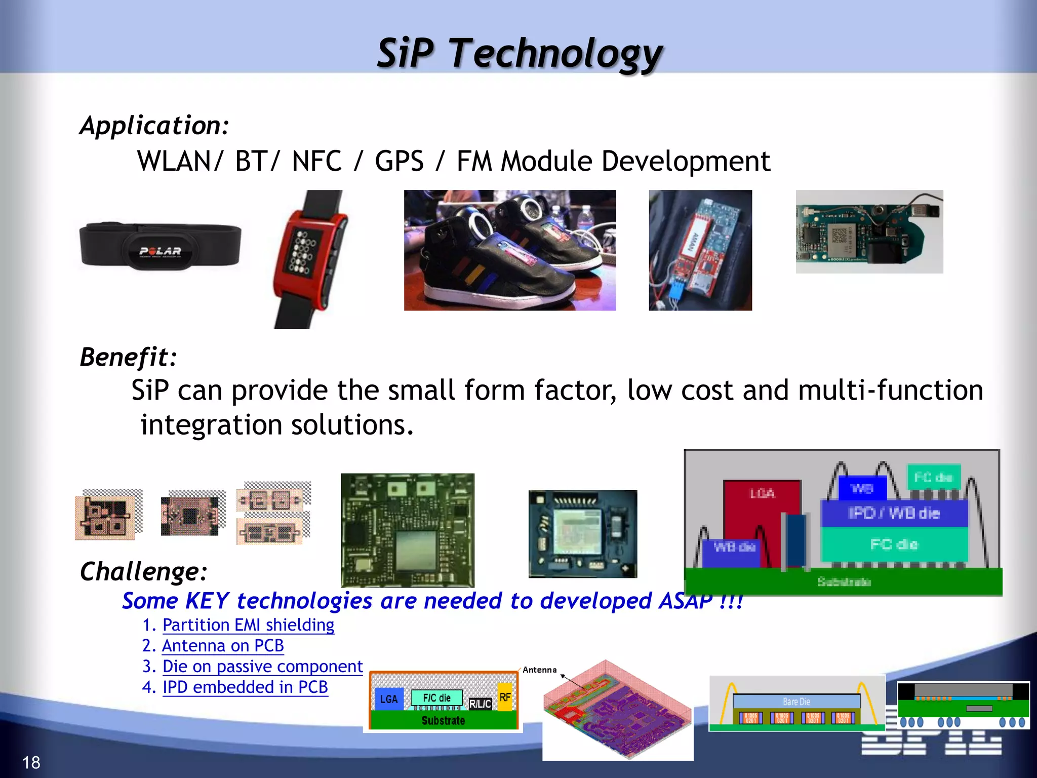
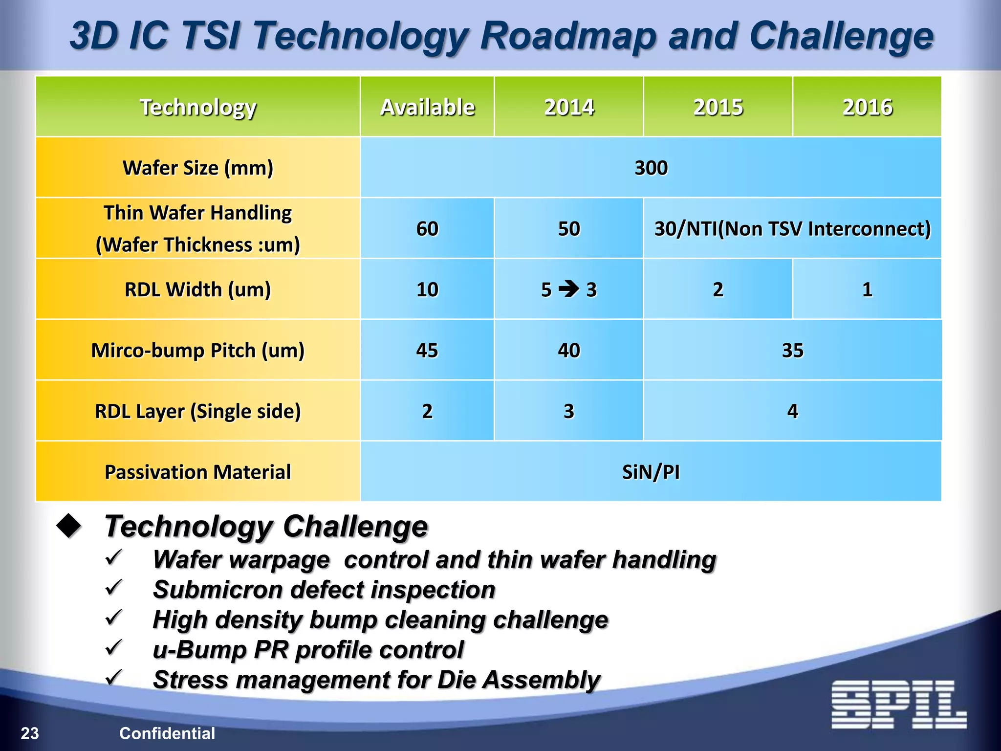
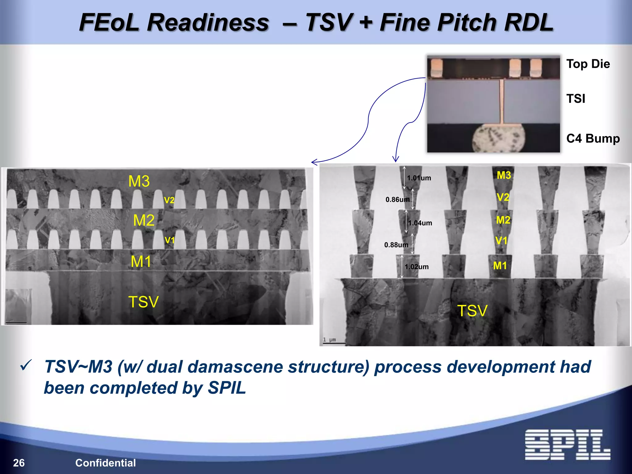
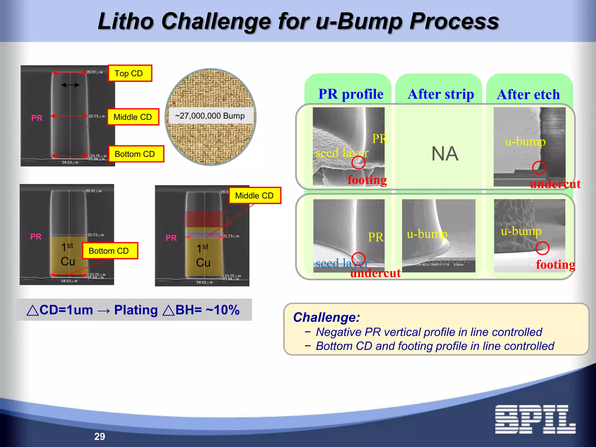
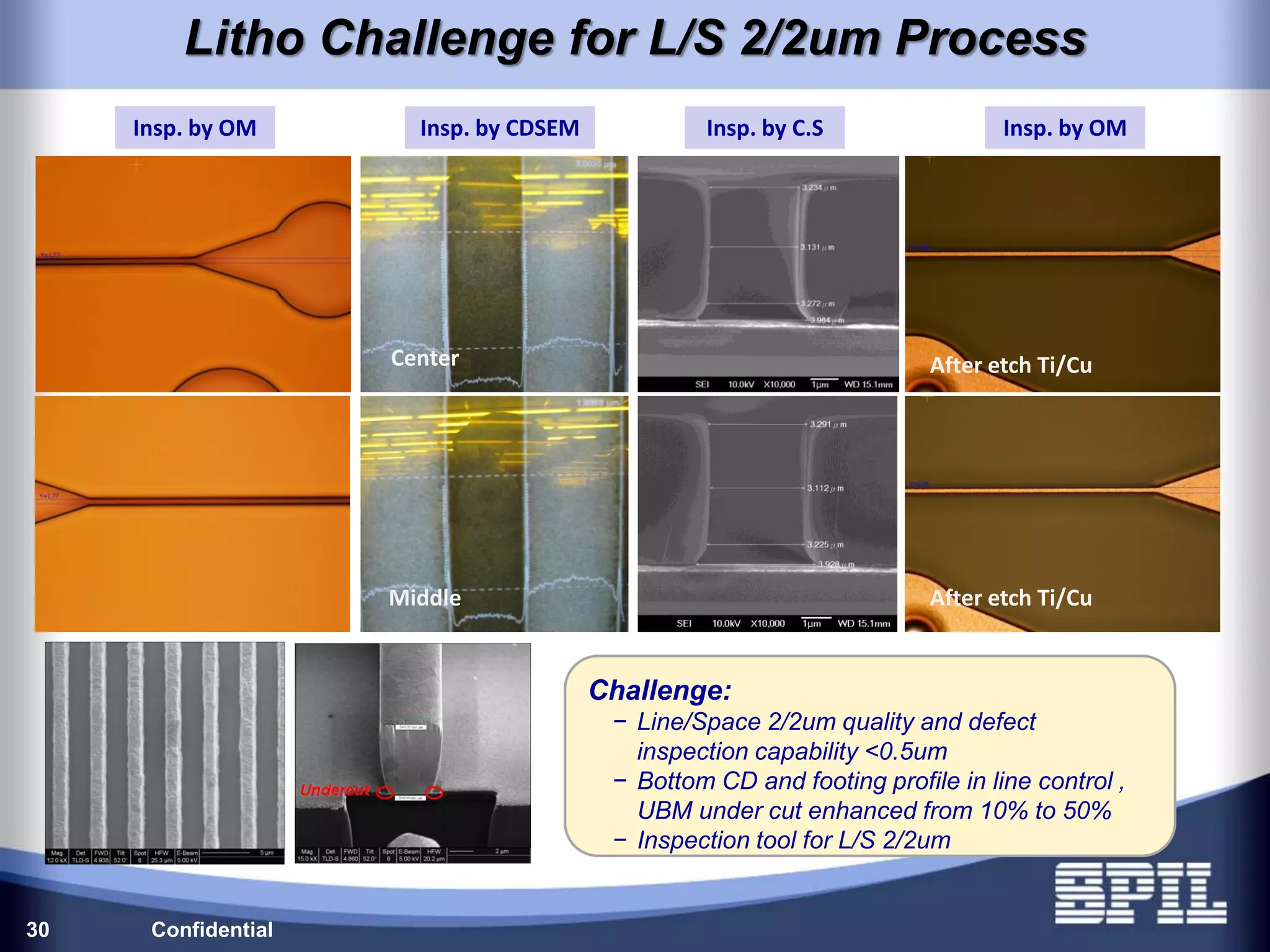
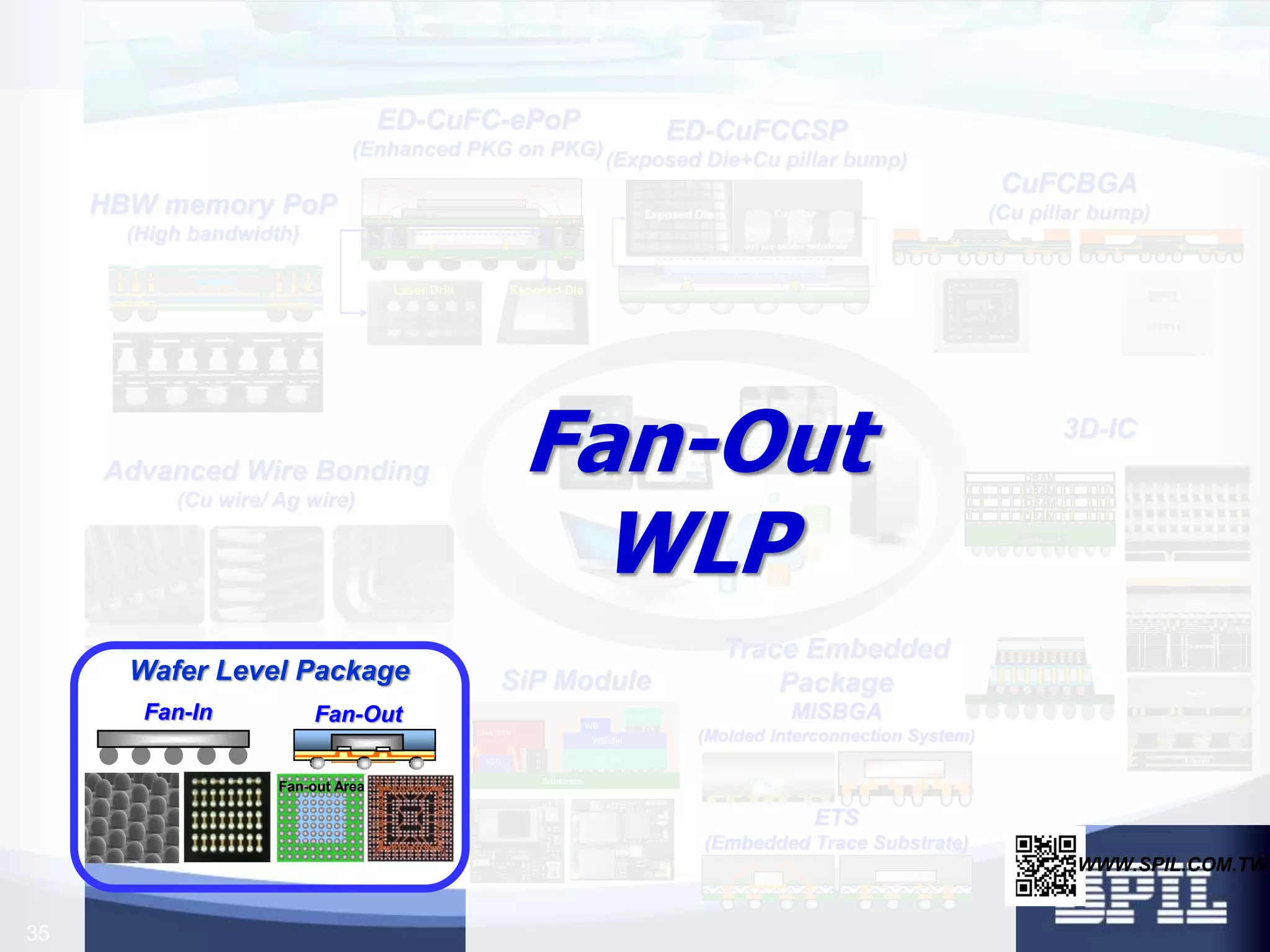
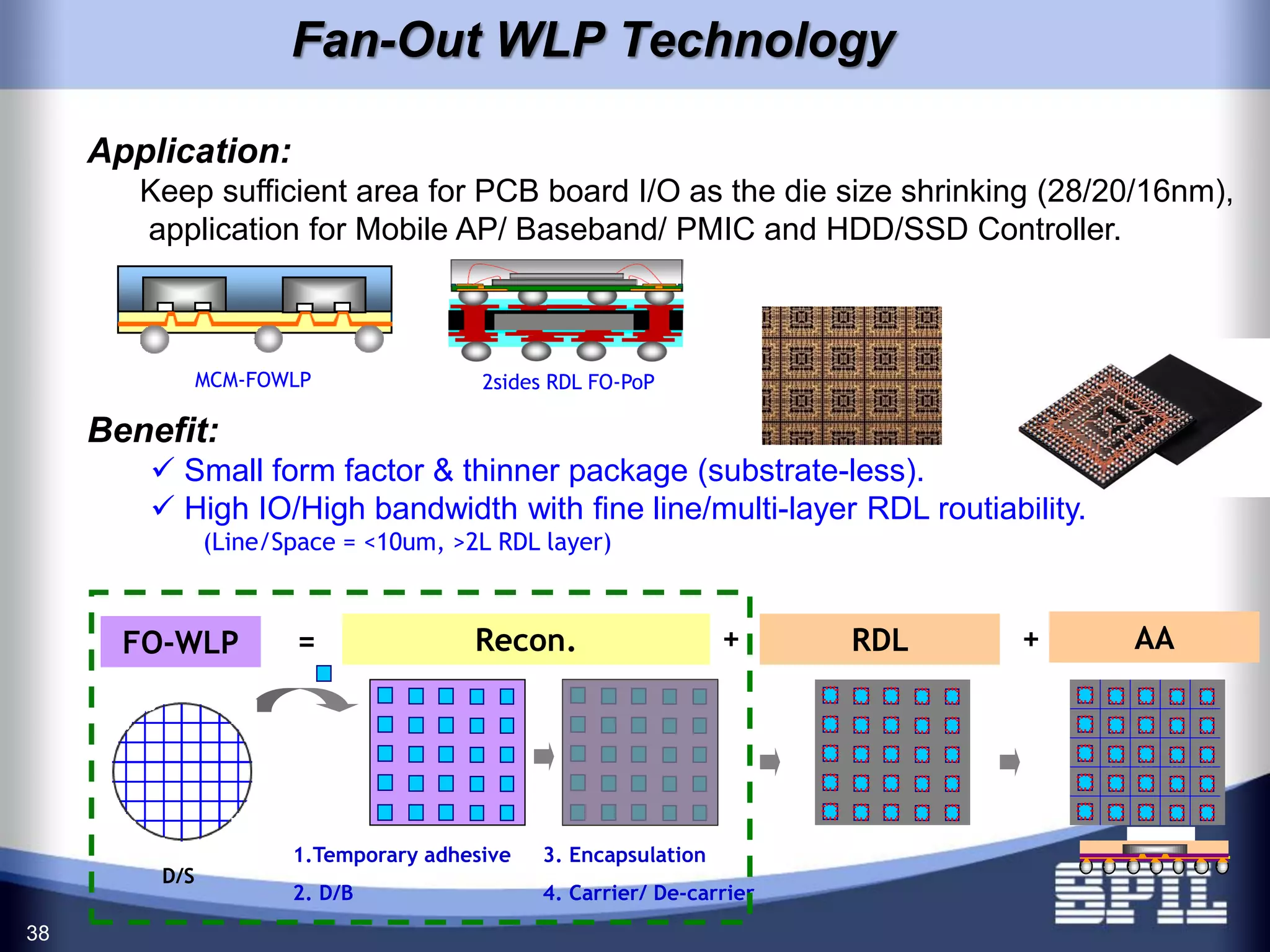
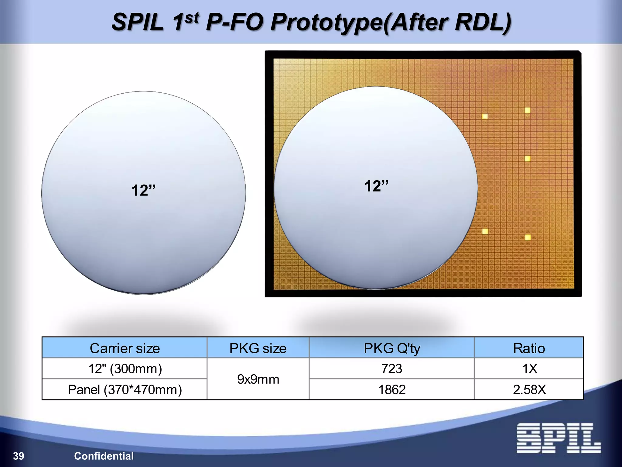
SiP Technology
Application:
WLAN/ BT/ NFC / GPS / FM Module Development
Benefit:
SiP can provide the small form factor, low cost and multi-function
integration solutions.
Challenge:
Some KEY technologies are needed to developed ASAP !!!
1. Partition EMI shielding
2. Antenna on PCB
3. Die on passive component
4. IPD embedded in PCB
18
CuFCBGA
(Cu pillar bump)
ED-CuFCCSP
(Exposed Die+Cu pillar bump)
Advanced Wire Bonding
(Cu wire/ Ag wire)
Wafer Level Package
Fan-In
LGA /QFN
WB FC die
WB die
WB
S
M
D
Substrate
FC die
LGA /QFN
WB FC die
WB die
WB
S
M
D
Substrate
FC die
LGA /QFN
WB FC die
WB die
WBWB
S
M
D
Substrate
FC die
SiP Module
WWW.SPIL.COM.TW
Fan-Out
Fan-out Area
HBW memory PoP
(High bandwidth)
ED-CuFC-ePoP
(Enhanced PKG on PKG)
Laser DrillLaser DrillLaser Drill Exposed Die
Trace Embedded
Package
MISBGA
(Molded Interconnection System)
ETS
(Embedded Trace Substrate)
3D-IC
Top die
TSI
Substrate
Substrate
DRAM
DRAM
DRAM
DRAM
Top die
TSI
Substrate
3D-IC
19
Confidential20
Memory
Logic
Fine Pitch
Micro Bump
2012 2013 2014
~~
3DIC Package Roadmap
Fine Pitch
Micro Joint
Structure
Heterogeneous Stacking
- Bridge multi function die
- Fully integrated package
3D Stacking
Heterogeneous Integration
2.5D Stacking
Silicon Interposer
Silicon Interposer
- Bridge ASIC to substrate
- Platform of high integrated MCM
- IPD integration (option)
3D DRAM Stacking
Analog / RF
Memory
Logic
TSI
Logic
Single Die
TSI
MemoryLogic
Multiple Die
Logic
TSI
Multiple Die
w/ Stacking DRAM
Substrate
DRAM
DRAM
DRAM
DRAM
3D Stacking DRAM
2015
~~
3DIC Product Performance
Confidential21
Source: Samsung
 By changing package from POP to 3D TSV
 Package Size : Reduce 35%
 Power Consumption : Reduce 50%
 Bandwidth : Increase 8X
Si interposer
Substrate
IC IC
Substrate
TSI
ASIC
DRAM
0.05~0.1um
Micro
Bump
Carrier
Bonding
Wafer
Thinning
CMP
RDL
TSV
Reveal
Die
Bonding
3DIC
Technology
TSV
Key Enabling Technology for 2.5/3DIC
Substrate
DRAM
DRAM
DRAM
DRAM
Confidential23
3D IC TSI Technology Roadmap and Challenge
Technology Available 2014 2015 2016
Wafer Size (mm) 300
Thin Wafer Handling
(Wafer Thickness :um)
60 50 30/NTI(Non TSV Interconnect)
RDL Width (um) 10 5  3 2 1
Mirco-bump Pitch (um) 45 40 35
RDL Layer (Single side) 2 3 4
Passivation Material SiN/PI
 Technology Challenge
 Wafer warpage control and thin wafer handling
 Submicron defect inspection
 High density bump cleaning challenge
 u-Bump PR profile control
 Stress management for Die Assembly
 Model B: Foundry+ SPIL
 Model A: Interposer processed by SPIL
SPIL’s Role in 2.5D/3D IC Supply Chain
Si interposer
Substrate
IC IC
Substrate
DRAM
DRAM
DRAM
DRAM
Memory
Logic
Substrate
or Memory
Logic IC
TSV + Front-side
Fine-Pitch RDL
Front-side
Micro-pad
Back-side
TSV Reveal
Back-side
RDL + Bump
Die Stacking &
Assembly
Test
Model A for 2.5D IC Fab
Model B for 2.5D/3D SPILIC Fab
MEoLProcess
Model
FEoL BEoL
SPIL
24 Confidential
 Good micro bump & c4 bump joint quality
Interposer
Substrate
DRAMGPU
Micro joint
C4 joint
Top die
TSI
Substrate
Top die
TSI
Substrate
TSI TSV
SPIL 2.5DIC Stacking Scheme
25 Confidential
Confidential26
FEoL Readiness – TSV + Fine Pitch RDL
 TSV~M3 (w/ dual damascene structure) process development had
been completed by SPIL
TSV
M1
V1
M2
V2
M3
TSV
M1
M2
M3
V1
V2
1.04um
0.88um
1.02um
0.86um
1.01um
Top Die
TSI
C4 Bump
Confidential27
Reflow
MEoL TSI Process: Wafer Bonding/De-bonding
Bonding&BVR process
Adh. Coating Carrier bonding Thinning
Carrier Carrier Carrier Carrier
Si etching SiN Dep.
Carrier
CMP
ReflowMetal Etching Taping
Tape
Carrier De-bonding
By Laser
Tape
Adh. Clean
CarrierCarrier
Carrier
Tape
De-bonding process
Challenge:
− Edge glue bleeding control, bubble inspection
− Defect induced by Plasma process
Challenge:
− Carrier glass back side surface defect control
− u-Bump/u-Pad quality control after De-bonding
Glass carrier
Adhesive layer
Release layer
Silicon
Confidential28
Glass 1
Adhesive
R/L
Silicon
Wafer Bond on Glass Challenge
 Definition of defect type
Defect Type
Performance Measured
method
Remark
Good (◎) Not bad (○) NG (×)
R/L Peeling
-The dark area: R/L still remained.
-The bright area: R/L has gone
Delamination
-Checked the delam by OM and
defined the delamination area
bubble
-Checked the edge performance
by OM
Bleeding
-Checked the edge performance
by OM
R/L
No R/L
Measurement point:
-Four point
OM checked:
Glue
bleeding
Carrier and wafer edge inspection
capability
Litho Challenge for u-Bump Process
29
~27,000,000 Bump
Bottom CD
Middle CD
Top CD
PR
PR
1st
Cu
PR
1st
Cu
Bottom CD
Middle CD
△CD=1um → Plating △BH= ~10%
Challenge:
− Negative PR vertical profile in line controlled
− Bottom CD and footing profile in line controlled
u-bump
undercut
PR profile
PR
seed layer
footing
PR
seed layer
After etchAfter strip
undercut
footing
u-bumpu-bump
NA
Confidential
After etch Ti/Cu
After etch Ti/Cu
30
Center
Middle
Insp. by OM Insp. by CDSEM Insp. by C.S Insp. by OM
Challenge:
− Line/Space 2/2um quality and defect
inspection capability <0.5um
− Bottom CD and footing profile in line control ,
UBM under cut enhanced from 10% to 50%
− Inspection tool for L/S 2/2um
Litho Challenge for L/S 2/2um Process
Confidential31
Chemical residue
High Density Bump Challenge for UBM Process
Lot ID Slot Structure
Yield loss of
PR residue
Yield loss of
metal residue
99D19285 1 uBump 13.37% 60.17%
Metal residue
Challenge:
− High density uBump PR removed
− Non-visible PR residue induced
UBM etching Metal residue
− Bump to bump bridge one die fail
− Inspection capability includes
>150um bump high
slot 1 2 3 4 5 6 7
WARP
Map
WARP 63 -46 -62 -94 -88 -121 -64
shape
slot 8 9 10 11 12 13 14
WARP
Map
WARP -39 54 93 58 69 85 93
shape
Si
Glue
Glass
Si
Glue
Glass
Si
Glue
Glass
Si
Glue
Glass
Si
Glue
Glass
Si
Glue
Glass
Si
Glue
Glass
Si
Glue
Glass
Si
Glue
Glass
Si
Glue
Glass
Si
Glue
Glass
Si
Glue
Glass
Si
Glue
Glass
Si
Glue
Glass
Challenge:
− Film stress management and warpage in line measurement
− Assure wafer process and Die warpage under controlled
Thin wafer Stress induced and Warpage Measured
Confidential33
Defect on
Bump top: non-wetting
Bump bottom: bump bridge
Missing bump
Defect images
Foreign material (on surface)
Foreign material (on bump top)
Blurred Blurred
Blurred
Clear Clear
Clear Clear Clear
• The defect on wafer surface (Missing
bump, F.M…) can be detected by both
of these recipes.
• Only 5X-DF mode can detect the tiny
residue on bump, and can see it
clearly by 20X-DF mode.
Challenge of u-Bump BEoL Stacking Inspection
Confidential34
Original New
* Light source
Focus on surface
Bright field
3X
Focus on bump top
5X or 10X
Focus plane
offset
Ring light
Focus plane
u-Bump Inspection on Top and Bottom
Challenge:
How to detect Bump top and bottom defect
in the same recipe?
CuFCBGA
(Cu pillar bump)
ED-CuFCCSP
(Exposed Die+Cu pillar bump)
Advanced Wire Bonding
(Cu wire/ Ag wire)
Wafer Level Package
Fan-In
LGA /QFN
WB FC die
WB die
WB
S
M
D
Substrate
FC die
LGA /QFN
WB FC die
WB die
WB
S
M
D
Substrate
FC die
LGA /QFN
WB FC die
WB die
WBWB
S
M
D
Substrate
FC die
SiP Module
WWW.SPIL.COM.TW
Fan-Out
Fan-out Area
HBW memory PoP
(High bandwidth)
ED-CuFC-ePoP
(Enhanced PKG on PKG)
Laser DrillLaser DrillLaser Drill Exposed Die
Trace Embedded
Package
MISBGA
(Molded Interconnection System)
ETS
(Embedded Trace Substrate)
3D-IC
Top die
TSI
Substrate
Substrate
DRAM
DRAM
DRAM
DRAM
Top die
TSI
Substrate
Fan-Out
WLP
35
Confidential36
Source: Yole
Roadmap Panel Level Embedding
Extreme Slim PoP Approaching
 PoP(3D Stacking)
 3L(Bot)+1L(Top) RDL
 L/S=5/5um~10/10um
 PKG Height<1.0mm
 High Bandwidth
 MCM/MCM-PoP
 3L(Bot)+1L(Top) RDL
 L/S=2/2um
 PKG Height<1.0mm
 LCI Alternative
Performance
L/S=2/2 & 3/3L/S=5/5~10/10
2013
L/S=15/15
FO-PoP (3L+1L) MCM-FOWLP (>2L)
FO-PoP (3L+1L)
 BD-PoP/ ePoP
 EPS/ ETS Coreless
 L/S=15/15um
 PKG Height >1.0mm
 0.5/0.4/0.27mm TBP
1.2~1.5
(mm)
<1.0
(mm)
Thin
PKG
Bare Die PoP
ePoP
37
Fan-Out WLP Technology
Application:
Keep sufficient area for PCB board I/O as the die size shrinking (28/20/16nm),
application for Mobile AP/ Baseband/ PMIC and HDD/SSD Controller.
Benefit:
 Small form factor & thinner package (substrate-less).
 High IO/High bandwidth with fine line/multi-layer RDL routiability.
(Line/Space = <10um, >2L RDL layer)
MCM-FOWLP 2sides RDL FO-PoP
38
D/S
1.Temporary adhesive
2. D/B
Recon. RDLFO-WLP +=
3. Encapsulation
4. Carrier/ De-carrier
AA+
Panel
Confidential39
SPIL 1st P-FO Prototype(After RDL)
12”
Carrier size PKG size PKG Q'ty Ratio
12" (300mm) 723 1X
Panel (370*470mm) 1862 2.58X
9x9mm
12”

從封測產業趨勢談設備需求與機會_ part2

  • 1.
    SiP Technology Application: WLAN/ BT/NFC / GPS / FM Module Development Benefit: SiP can provide the small form factor, low cost and multi-function integration solutions. Challenge: Some KEY technologies are needed to developed ASAP !!! 1. Partition EMI shielding 2. Antenna on PCB 3. Die on passive component 4. IPD embedded in PCB 18
  • 2.
    CuFCBGA (Cu pillar bump) ED-CuFCCSP (ExposedDie+Cu pillar bump) Advanced Wire Bonding (Cu wire/ Ag wire) Wafer Level Package Fan-In LGA /QFN WB FC die WB die WB S M D Substrate FC die LGA /QFN WB FC die WB die WB S M D Substrate FC die LGA /QFN WB FC die WB die WBWB S M D Substrate FC die SiP Module WWW.SPIL.COM.TW Fan-Out Fan-out Area HBW memory PoP (High bandwidth) ED-CuFC-ePoP (Enhanced PKG on PKG) Laser DrillLaser DrillLaser Drill Exposed Die Trace Embedded Package MISBGA (Molded Interconnection System) ETS (Embedded Trace Substrate) 3D-IC Top die TSI Substrate Substrate DRAM DRAM DRAM DRAM Top die TSI Substrate 3D-IC 19
  • 3.
    Confidential20 Memory Logic Fine Pitch Micro Bump 20122013 2014 ~~ 3DIC Package Roadmap Fine Pitch Micro Joint Structure Heterogeneous Stacking - Bridge multi function die - Fully integrated package 3D Stacking Heterogeneous Integration 2.5D Stacking Silicon Interposer Silicon Interposer - Bridge ASIC to substrate - Platform of high integrated MCM - IPD integration (option) 3D DRAM Stacking Analog / RF Memory Logic TSI Logic Single Die TSI MemoryLogic Multiple Die Logic TSI Multiple Die w/ Stacking DRAM Substrate DRAM DRAM DRAM DRAM 3D Stacking DRAM 2015 ~~
  • 4.
    3DIC Product Performance Confidential21 Source:Samsung  By changing package from POP to 3D TSV  Package Size : Reduce 35%  Power Consumption : Reduce 50%  Bandwidth : Increase 8X
  • 5.
  • 6.
    Confidential23 3D IC TSITechnology Roadmap and Challenge Technology Available 2014 2015 2016 Wafer Size (mm) 300 Thin Wafer Handling (Wafer Thickness :um) 60 50 30/NTI(Non TSV Interconnect) RDL Width (um) 10 5  3 2 1 Mirco-bump Pitch (um) 45 40 35 RDL Layer (Single side) 2 3 4 Passivation Material SiN/PI  Technology Challenge  Wafer warpage control and thin wafer handling  Submicron defect inspection  High density bump cleaning challenge  u-Bump PR profile control  Stress management for Die Assembly
  • 7.
     Model B:Foundry+ SPIL  Model A: Interposer processed by SPIL SPIL’s Role in 2.5D/3D IC Supply Chain Si interposer Substrate IC IC Substrate DRAM DRAM DRAM DRAM Memory Logic Substrate or Memory Logic IC TSV + Front-side Fine-Pitch RDL Front-side Micro-pad Back-side TSV Reveal Back-side RDL + Bump Die Stacking & Assembly Test Model A for 2.5D IC Fab Model B for 2.5D/3D SPILIC Fab MEoLProcess Model FEoL BEoL SPIL 24 Confidential
  • 8.
     Good microbump & c4 bump joint quality Interposer Substrate DRAMGPU Micro joint C4 joint Top die TSI Substrate Top die TSI Substrate TSI TSV SPIL 2.5DIC Stacking Scheme 25 Confidential
  • 9.
    Confidential26 FEoL Readiness –TSV + Fine Pitch RDL  TSV~M3 (w/ dual damascene structure) process development had been completed by SPIL TSV M1 V1 M2 V2 M3 TSV M1 M2 M3 V1 V2 1.04um 0.88um 1.02um 0.86um 1.01um Top Die TSI C4 Bump
  • 10.
    Confidential27 Reflow MEoL TSI Process:Wafer Bonding/De-bonding Bonding&BVR process Adh. Coating Carrier bonding Thinning Carrier Carrier Carrier Carrier Si etching SiN Dep. Carrier CMP ReflowMetal Etching Taping Tape Carrier De-bonding By Laser Tape Adh. Clean CarrierCarrier Carrier Tape De-bonding process Challenge: − Edge glue bleeding control, bubble inspection − Defect induced by Plasma process Challenge: − Carrier glass back side surface defect control − u-Bump/u-Pad quality control after De-bonding Glass carrier Adhesive layer Release layer Silicon
  • 11.
    Confidential28 Glass 1 Adhesive R/L Silicon Wafer Bondon Glass Challenge  Definition of defect type Defect Type Performance Measured method Remark Good (◎) Not bad (○) NG (×) R/L Peeling -The dark area: R/L still remained. -The bright area: R/L has gone Delamination -Checked the delam by OM and defined the delamination area bubble -Checked the edge performance by OM Bleeding -Checked the edge performance by OM R/L No R/L Measurement point: -Four point OM checked: Glue bleeding Carrier and wafer edge inspection capability
  • 12.
    Litho Challenge foru-Bump Process 29 ~27,000,000 Bump Bottom CD Middle CD Top CD PR PR 1st Cu PR 1st Cu Bottom CD Middle CD △CD=1um → Plating △BH= ~10% Challenge: − Negative PR vertical profile in line controlled − Bottom CD and footing profile in line controlled u-bump undercut PR profile PR seed layer footing PR seed layer After etchAfter strip undercut footing u-bumpu-bump NA
  • 13.
    Confidential After etch Ti/Cu Afteretch Ti/Cu 30 Center Middle Insp. by OM Insp. by CDSEM Insp. by C.S Insp. by OM Challenge: − Line/Space 2/2um quality and defect inspection capability <0.5um − Bottom CD and footing profile in line control , UBM under cut enhanced from 10% to 50% − Inspection tool for L/S 2/2um Litho Challenge for L/S 2/2um Process
  • 14.
    Confidential31 Chemical residue High DensityBump Challenge for UBM Process Lot ID Slot Structure Yield loss of PR residue Yield loss of metal residue 99D19285 1 uBump 13.37% 60.17% Metal residue Challenge: − High density uBump PR removed − Non-visible PR residue induced UBM etching Metal residue − Bump to bump bridge one die fail − Inspection capability includes >150um bump high
  • 15.
    slot 1 23 4 5 6 7 WARP Map WARP 63 -46 -62 -94 -88 -121 -64 shape slot 8 9 10 11 12 13 14 WARP Map WARP -39 54 93 58 69 85 93 shape Si Glue Glass Si Glue Glass Si Glue Glass Si Glue Glass Si Glue Glass Si Glue Glass Si Glue Glass Si Glue Glass Si Glue Glass Si Glue Glass Si Glue Glass Si Glue Glass Si Glue Glass Si Glue Glass Challenge: − Film stress management and warpage in line measurement − Assure wafer process and Die warpage under controlled Thin wafer Stress induced and Warpage Measured
  • 16.
    Confidential33 Defect on Bump top:non-wetting Bump bottom: bump bridge Missing bump Defect images Foreign material (on surface) Foreign material (on bump top) Blurred Blurred Blurred Clear Clear Clear Clear Clear • The defect on wafer surface (Missing bump, F.M…) can be detected by both of these recipes. • Only 5X-DF mode can detect the tiny residue on bump, and can see it clearly by 20X-DF mode. Challenge of u-Bump BEoL Stacking Inspection
  • 17.
    Confidential34 Original New * Lightsource Focus on surface Bright field 3X Focus on bump top 5X or 10X Focus plane offset Ring light Focus plane u-Bump Inspection on Top and Bottom Challenge: How to detect Bump top and bottom defect in the same recipe?
  • 18.
    CuFCBGA (Cu pillar bump) ED-CuFCCSP (ExposedDie+Cu pillar bump) Advanced Wire Bonding (Cu wire/ Ag wire) Wafer Level Package Fan-In LGA /QFN WB FC die WB die WB S M D Substrate FC die LGA /QFN WB FC die WB die WB S M D Substrate FC die LGA /QFN WB FC die WB die WBWB S M D Substrate FC die SiP Module WWW.SPIL.COM.TW Fan-Out Fan-out Area HBW memory PoP (High bandwidth) ED-CuFC-ePoP (Enhanced PKG on PKG) Laser DrillLaser DrillLaser Drill Exposed Die Trace Embedded Package MISBGA (Molded Interconnection System) ETS (Embedded Trace Substrate) 3D-IC Top die TSI Substrate Substrate DRAM DRAM DRAM DRAM Top die TSI Substrate Fan-Out WLP 35
  • 19.
  • 20.
    Extreme Slim PoPApproaching  PoP(3D Stacking)  3L(Bot)+1L(Top) RDL  L/S=5/5um~10/10um  PKG Height<1.0mm  High Bandwidth  MCM/MCM-PoP  3L(Bot)+1L(Top) RDL  L/S=2/2um  PKG Height<1.0mm  LCI Alternative Performance L/S=2/2 & 3/3L/S=5/5~10/10 2013 L/S=15/15 FO-PoP (3L+1L) MCM-FOWLP (>2L) FO-PoP (3L+1L)  BD-PoP/ ePoP  EPS/ ETS Coreless  L/S=15/15um  PKG Height >1.0mm  0.5/0.4/0.27mm TBP 1.2~1.5 (mm) <1.0 (mm) Thin PKG Bare Die PoP ePoP 37
  • 21.
    Fan-Out WLP Technology Application: Keepsufficient area for PCB board I/O as the die size shrinking (28/20/16nm), application for Mobile AP/ Baseband/ PMIC and HDD/SSD Controller. Benefit:  Small form factor & thinner package (substrate-less).  High IO/High bandwidth with fine line/multi-layer RDL routiability. (Line/Space = <10um, >2L RDL layer) MCM-FOWLP 2sides RDL FO-PoP 38 D/S 1.Temporary adhesive 2. D/B Recon. RDLFO-WLP += 3. Encapsulation 4. Carrier/ De-carrier AA+
  • 22.
    Panel Confidential39 SPIL 1st P-FOPrototype(After RDL) 12” Carrier size PKG size PKG Q'ty Ratio 12" (300mm) 723 1X Panel (370*470mm) 1862 2.58X 9x9mm 12”