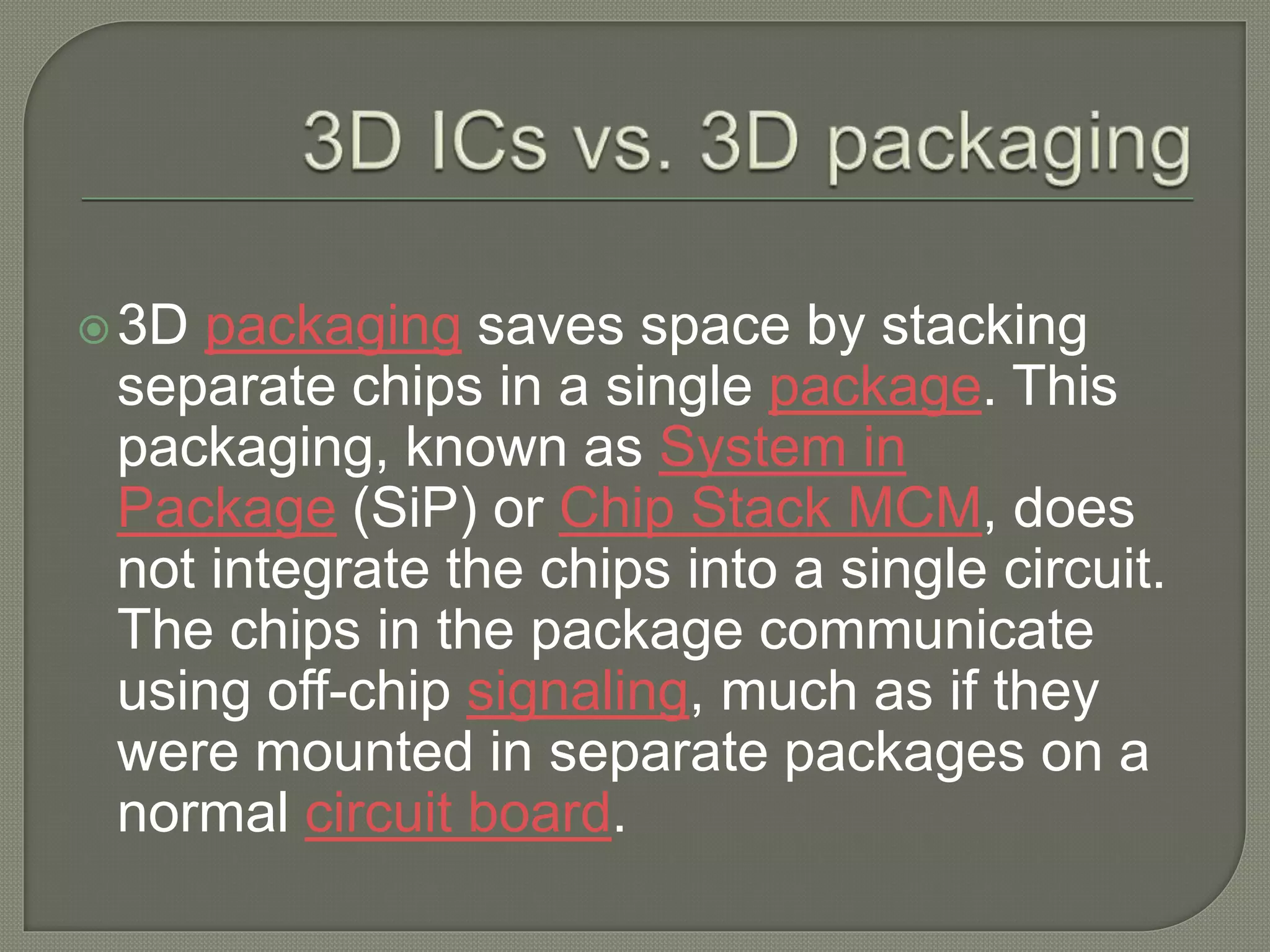
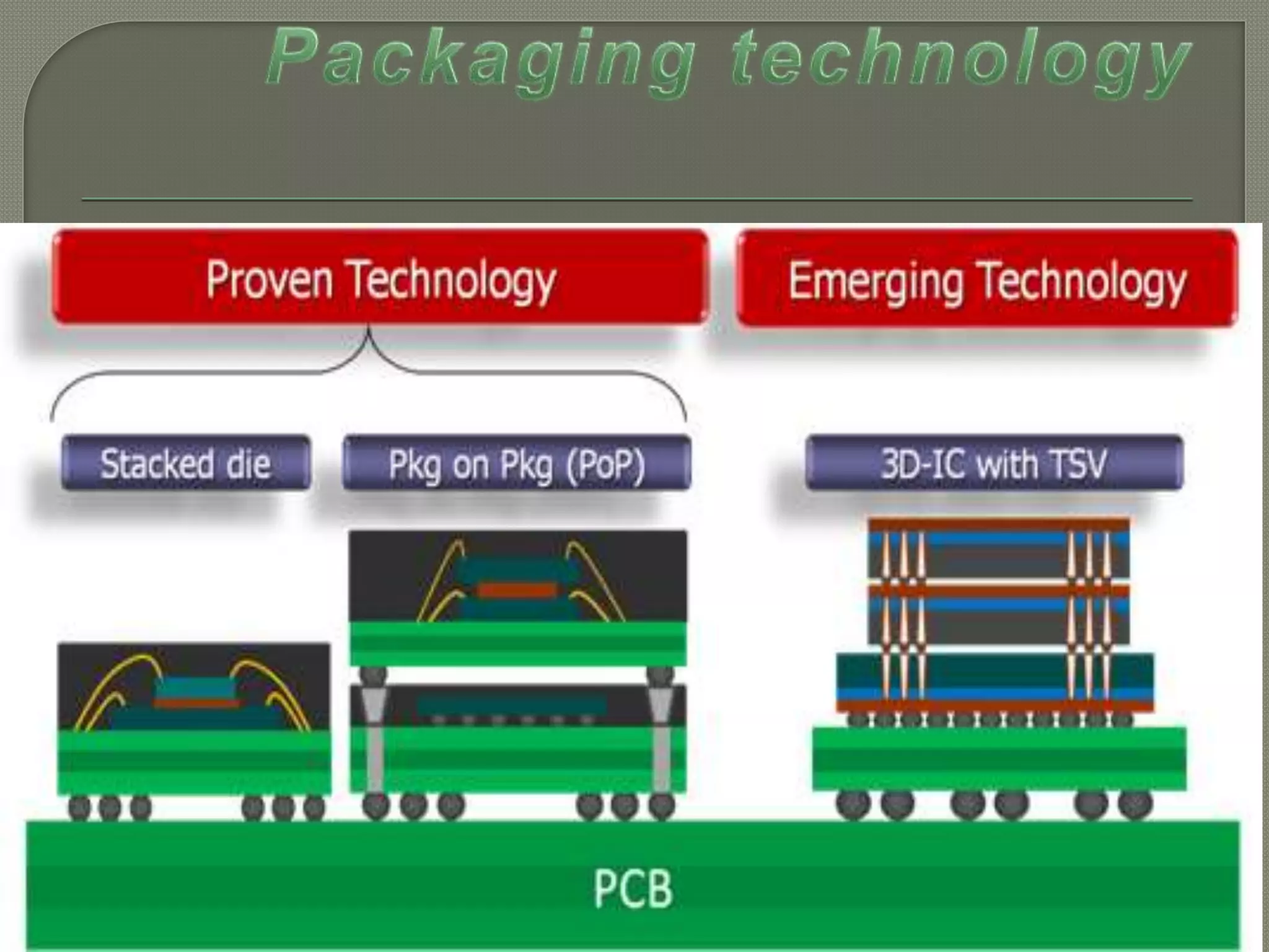
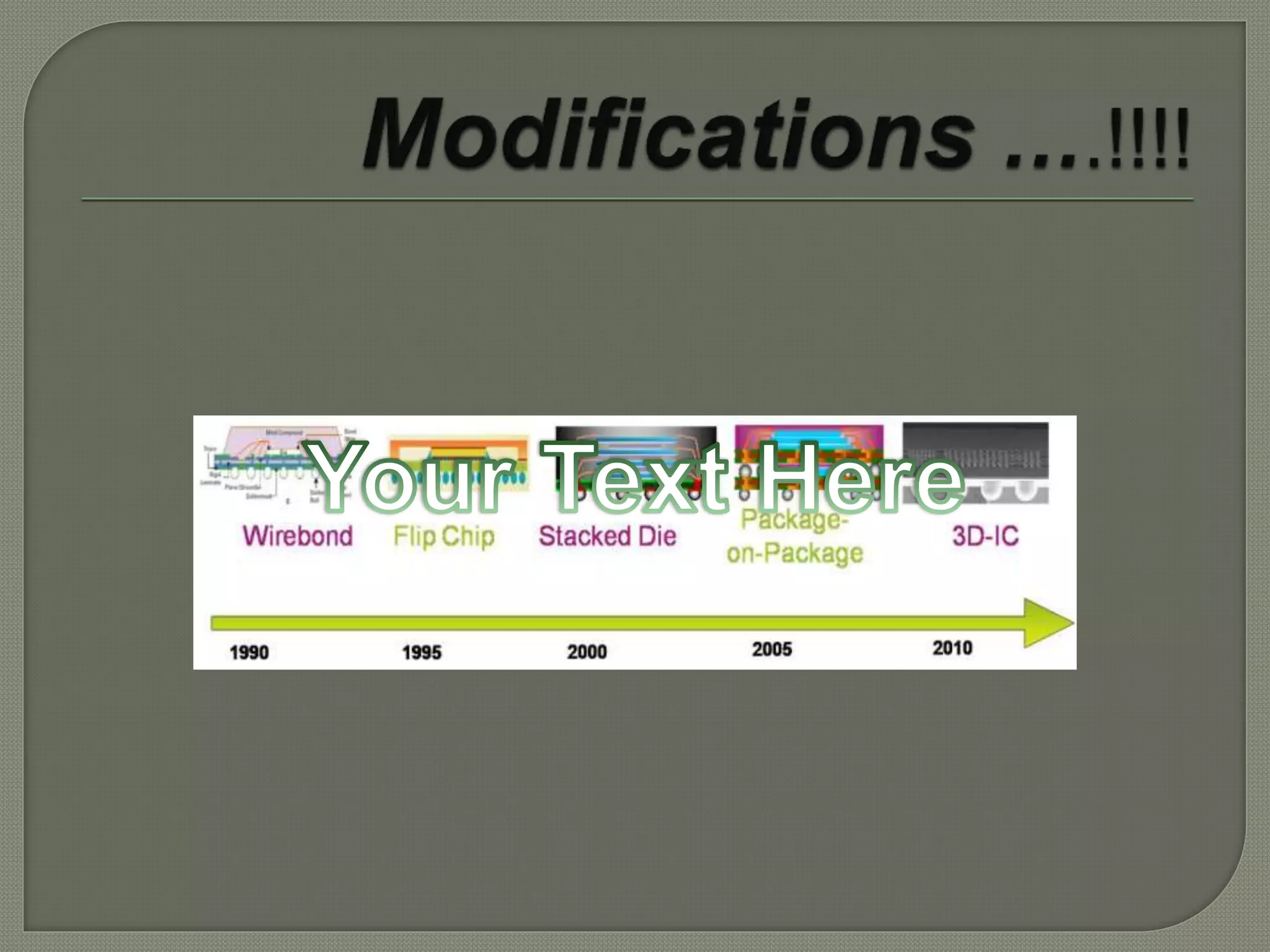
3D packaging stacks separate chips in a single package to save space without integrating the chips. Monolithic 3D ICs build components in layers on a single wafer then dice it, avoiding alignment and bonding issues. Multi-wafer 3D ICs build components on separate wafers, which must be aligned, bonded, and thinned with vertical connections added through silicon vias. 3D ICs promise benefits like reduced cost from improved yield, lower power from shorter wires, and new design possibilities from added connectivity, but challenges include heat dissipation, design complexity, and testing of independent dies.
![ Traditional scaling of semiconductor chips also improves
signal propagation speed. 3-D integrated circuits were
invented to address the scaling challenge by stacking 2-
D dies and connecting them in the 3rd dimension. This
promises to speed up communication between layered
chips, compared to planar layout.[9] 3D ICs promise many
significant benefits, including:
Cost:
Partitioning a large chip into multiple smaller dies with 3D
stacking can improve the yield and reduce the fabrication
cost if individual dies are tested separately.[10][11]](https://image.slidesharecdn.com/3dicsvs-141118090448-conversion-gate02/75/3d-ic-s-ppt-7-2048.jpg)
![. Testing-
To achieve high overall yield and reduce costs, separate testing
of independent dies is essential.[3][19] However, tight integration
between adjacent active layers in 3D ICs entails a significant
amount of interconnect between different sections of the same
circuit module that were partitioned to different dies. Aside from
the massive overhead introduced by required TSVs, sections of
such a module, e.g., a multiplier, cannot be independently tested
by conventional techniques. This particularly applies to timing-critical
paths laid out in 3D.
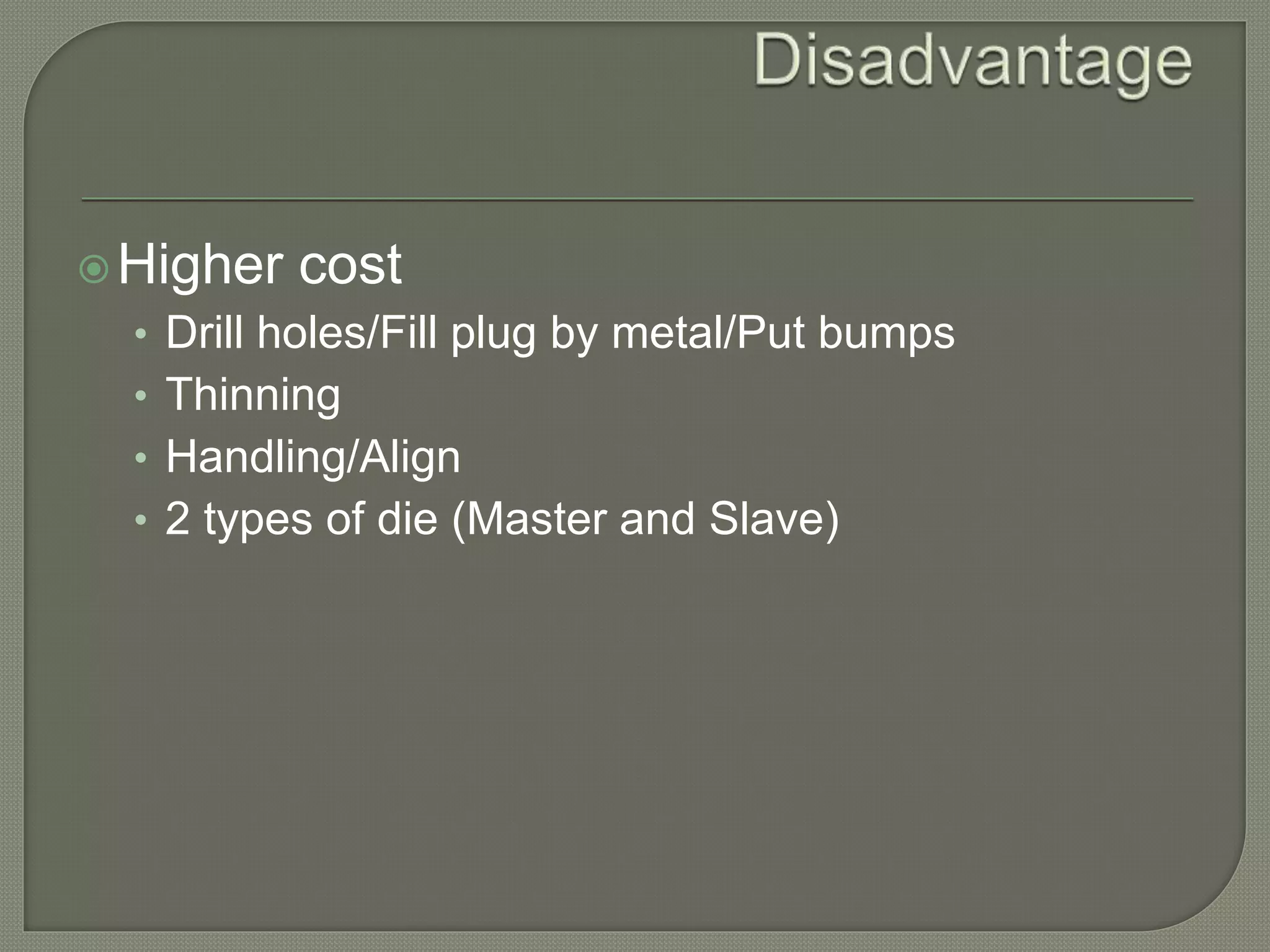
Yield-
Each extra manufacturing step adds a risk for defects. In order for
3D ICs to be commercially viable, defects could be repaired or
tolerated, or defect density can be improved.](https://image.slidesharecdn.com/3dicsvs-141118090448-conversion-gate02/75/3d-ic-s-ppt-11-2048.jpg)