
Recommended
More Related Content
What's hot
What's hot (20)
Similar to Three dimensional integrated circuit
Similar to Three dimensional integrated circuit (20)
Recently uploaded
Recently uploaded (20)
Three dimensional integrated circuit
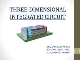
- 1. THREE-DIMENSIONAL INTEGRATED CIRCUIT ARQAM FAZAL MIRZA ROLL NO.:-1140434009 EC-3, BBD UNIVERSITY 1
- 2. CONTENTS INTRODUCTION WHAT IS TSV? MAKING OF TSV MANUFACTURING OF 3D-IC 3D VS 2D CIRCUIT WHY 3D OVER 2D-CIRCUIT? CHALLENGES NOTABLE 3D CHIPS CONCLUSION REFERENCES 2
- 3. INTRODUCTION 3D-IC is a circuit formed by the stacking silicon wafers/dies and interconnecting them vertically with the help of TSVs so they behave as a single device to achieve performance improvements at reduced power . Fig. 1 3
- 4. INTRODUCTION 3D-ICs offer significant improvements over 2D circuits as it reduces both the footprint and interconnect length without shrinking the resistors Fig.2 4
- 5. WHAT IS TSV? Through-silicon via, in electronic engineering, is a vertical electrical connection passing completely through a silicon wafer/die. It allows to establish an electrical connection from the active side to the backside of the die/wafer. Fig.3 5
- 6. WHAT IS TSV? TSVs are a high performance interconnect techniques used as an alternative to wire-bond and flip chips to create 3D packages and 3D integrated circuits because the density of vias is substantially higher, and because the length of connections in shorter. Fig.4 6
- 7. MAKING OF TSV In order to make a TSV, the following processes are done :- • Via Drilling • Via Filling • Chemical and mechanical polishing • TSV revealing 7
- 9. MANUFACTURING OF 3D-IC • A 3D-IC can be manufactured in the same manner as a normal 2D-Circuit • Multiple 2D-Circuits are formed in order to form a 3D-IC • Then these multiple circuits are joined together using the TSV technology Fig.6 9
- 10. MANUFACTURING OF 3D-IC • Only one power supply is needed for one 3D-IC • Different power supplies for different layers are not required Fig.7 10
- 11. 3D VS 2D CIRCUIT 2D 3D DIFFEREN CE (%) • Footprint (in sq.mm) 2.54 1.31 -48.4 • Wirelength (in mm) 3.41 3.19 -6.4 • Power (in mW) 172.9 164.0 -5.1 11
- 12. WHY 3D-IC OVER 2D-IC? • FOOTPRINT • COST • SHORTER INTERCONNECT • POWER 12
- 13. CHALLENGES • YIELD • HEAT • DESIGN COMPLEXITY • TESTING 13
- 14. NOTABLE 3D-CHIPS • Tezzeron Semiconductors built a 3D chip in 2004. The first chip was a simple memory register, but the most notable being an 8051 processor/memory stack. • INTEL presented a 3D version of Pentium 4 processor named as Pentium 4 Remix in 2004. • Samsung announced in December, 2008 that it has started the mass production of 8GB memory using 3D technology. 14
- 15. CONCLUSION • 3D technology is a technology which will bring a revolution in the industry. • In an era where smaller devices are preferred over large devices, a 3D-technology can help multiple circuits fit into a space where only one 2D-Circuit can fit. • Imagine how great it will be when a 64 or 128 GB of memory can be installed in a device which occupies a space less than a 8 GB memory. 15
- 16. REFERENCES • “ELECTRONIC DESIGN AUTOMATION FOR IC IMPLEMENTATION CIRCUIT DESIGN, AND PROCESS TECHNOLOGY” BY- LUCIANO LAVANGO (CRC PRESS) • “TSV(THROUGH SILICON VIA)” BY- ALKITA ELPIDA MEMORY ISSUED ON 08/11/2008 • “DEVELOPMENT OF CHIP STACKING TECHNOLOGY USING THROUGH ELECTRODES” VOL.74#3 BY-OKI TECHNICAL REVIEW NOV.,2007 ISSUE 16
- 17. QUERIES?? 17
- 18. THANK YOU 18