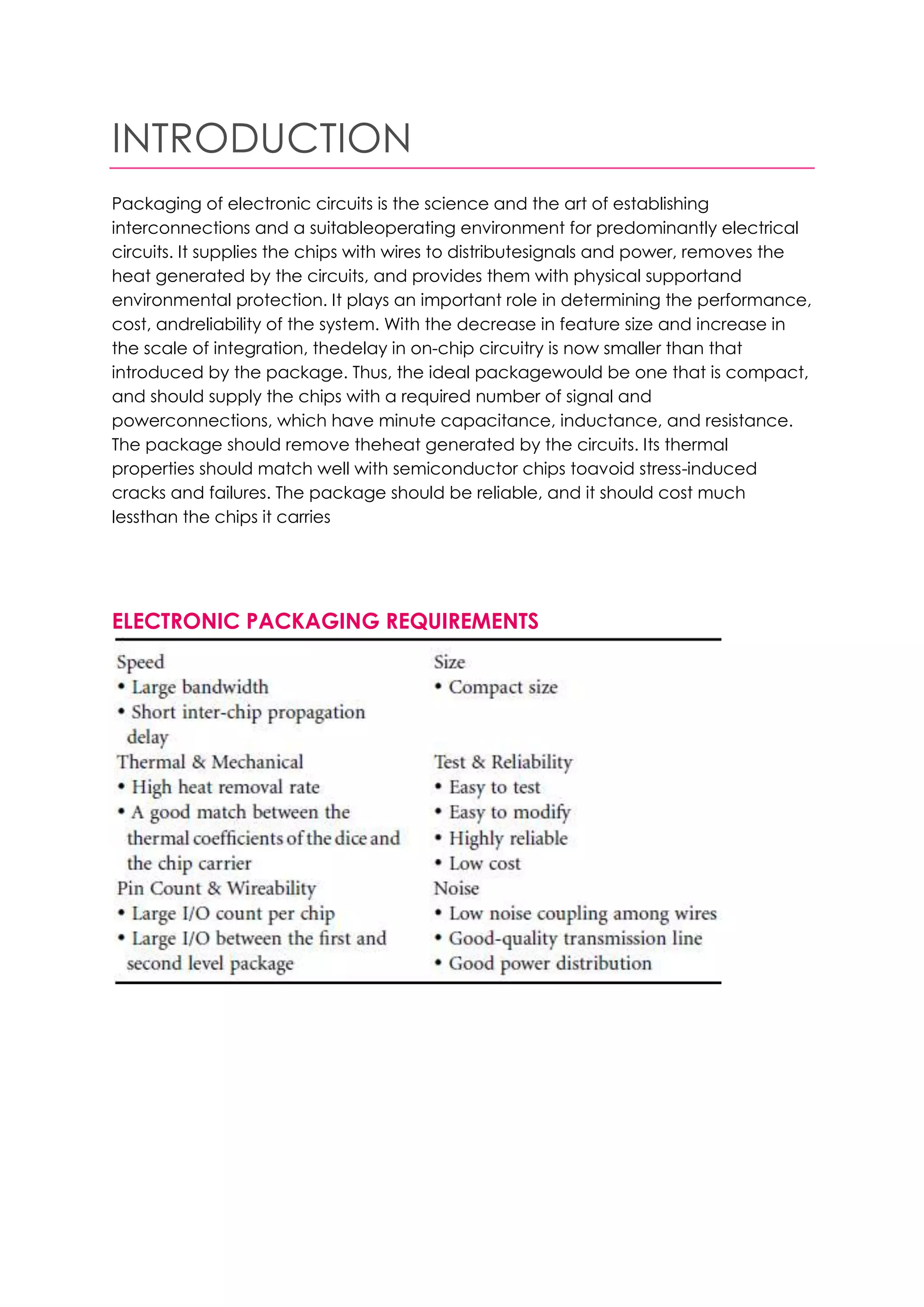
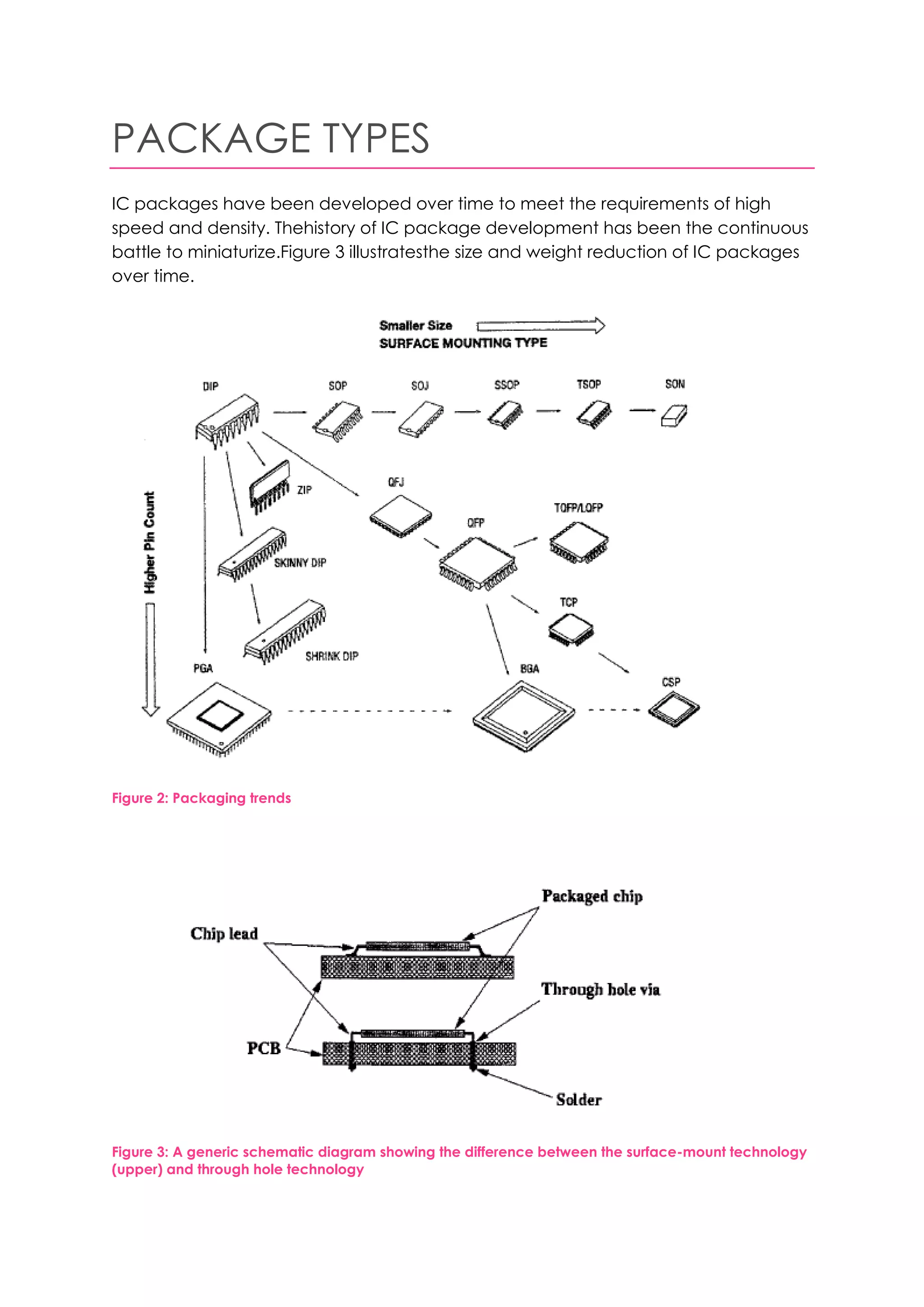
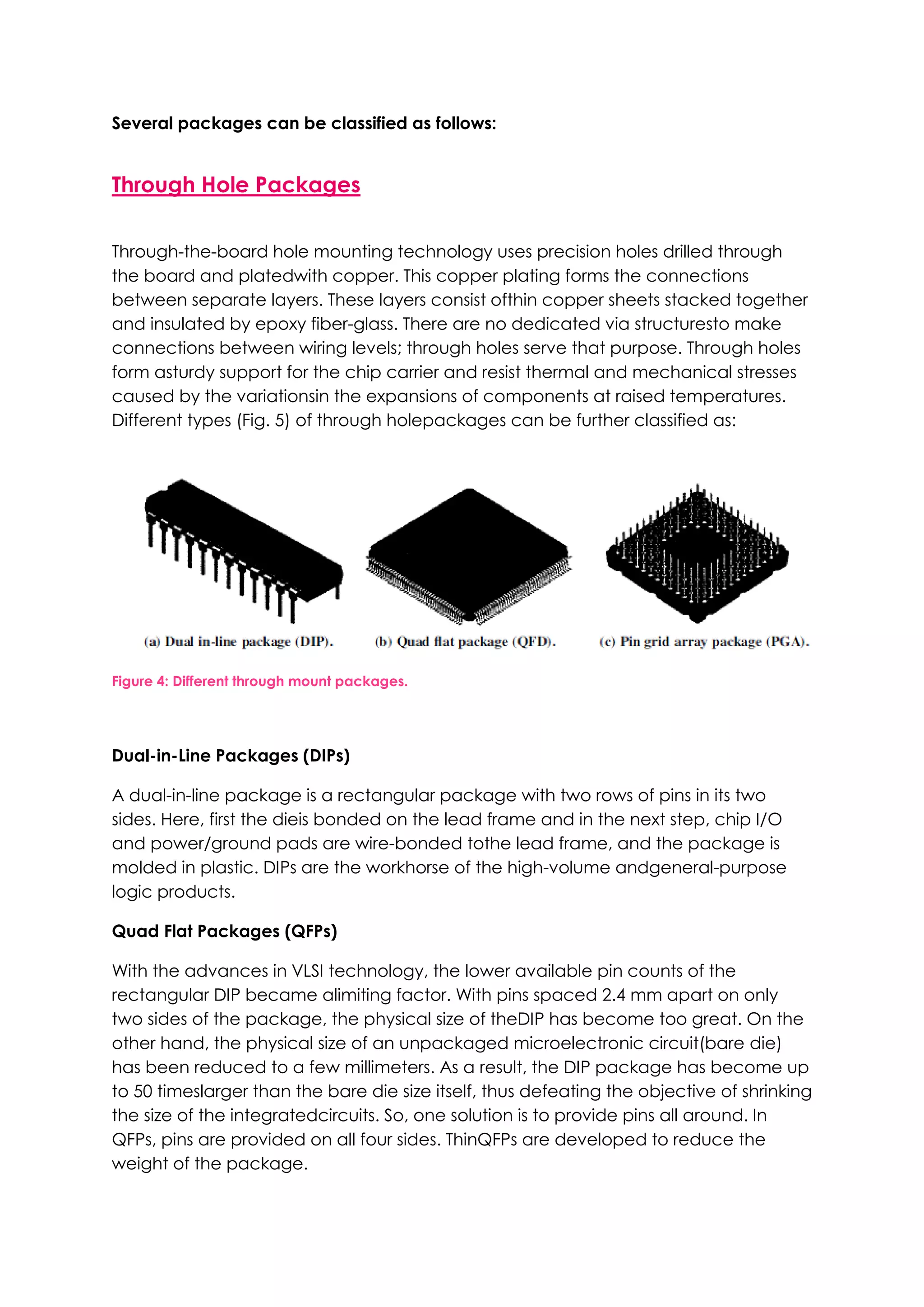
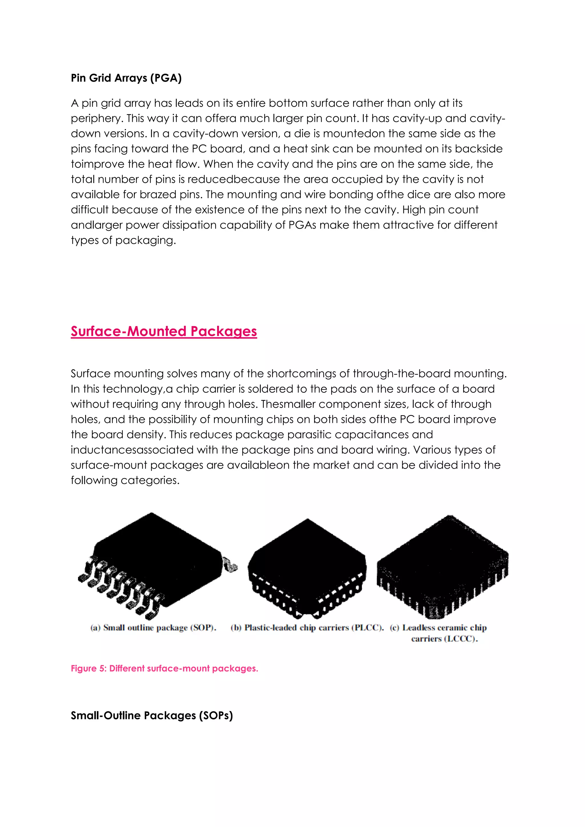
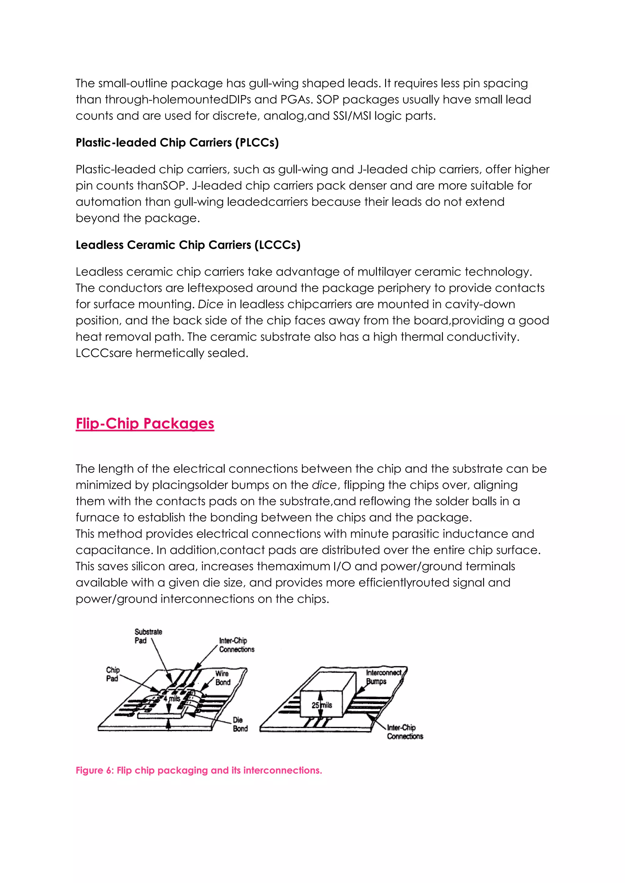
This document discusses packaging considerations for VLSI devices. It covers package types like through-hole packages, surface-mounted packages, flip chip packages, and chip-scale packages. Key package design considerations include the number of terminals, electrical design to minimize signal degradation, thermal design to dissipate heat, reliability over temperature cycles, and testability to ensure quality. The ideal package is compact with low-inductance connections to transfer heat efficiently while withstanding stresses.
This document discusses package design considerations and types of semiconductor packages. It covers key factors in package design like the number of terminals, electrical, thermal, and reliability requirements. The main package types discussed are through-hole packages like DIP and QFP, and surface mount packages like SOP, PLCC, and LCCC. Through-hole packages use precision holes drilled through the board while surface mount packages solder directly to the board surface.
The document discusses various integrated circuit packaging technologies. It describes through-hole packages, surface mount packages, chip-scale packages including wire bonded ball grid arrays and flip chip ball grid arrays. It then focuses on wafer level chip-scale packages, explaining that they are manufactured by building up interconnect structures directly on the silicon wafer before dicing. Key advantages of wafer level chip-scale packages are their small size, minimized inductance, and streamlined manufacturing process.
The document discusses the physical design process for VLSI circuits. It describes the main steps as partitioning, floor planning and placement, routing, layout optimization, and extraction and verification. The goals of physical design are to minimize signal delays, interconnection area, and power usage. Physical design transforms the logical structure of a circuit into its physical layout.
Routing in Integrated circuits is an important task which requires extreme care while placing the modules and circuits and connecting them with each other.
System partitioning in VLSI and its considerationsSubash John
System partitioning divides a large circuit into smaller subcircuits. This allows the subcircuits to be designed independently and in parallel, speeding up the design process. Effective partitioning aims to minimize connections between subcircuits. Tool-based partitioning allows constraints to be set to generate a partitioned netlist that balances subcircuit sizes and minimizes connections between top-level blocks.
This document discusses chip packaging technology. It explains that chip packaging brings signal and power connections out of the silicon die while also protecting the die from environmental conditions and dissipating heat. The document covers key aspects of chip packaging like Rent's rule, material selection, interconnect levels, multichip modules, thermal considerations, and trends in packaging technologies. It provides an overview of chip packaging objectives and requirements.
The document discusses VLSI assembly technology and the fabrication process for integrated circuits. It describes the key steps in assembly such as wafer back grinding, die preparation, die bonding, wire bonding, flip chip bonding, molding, package sealing, marking, and singulation. It also summarizes the major steps in IC fabrication including silicon crystal growth, lithography, oxidation, etching, diffusion/implantation, and annealing.
1) The document discusses the Metal-Oxide-Semiconductor (MOS) capacitor, which is important for understanding MOSFET operation.
2) It describes the energy band diagrams and carrier accumulation, depletion, and inversion in MOS capacitors under different bias conditions for both p-type and n-type semiconductor substrates.
3) Key concepts covered include the flat-band voltage, threshold voltage, effects of oxide charges, and maximum depletion width.
The document discusses the fabrication process of MOSFET transistors. It begins by introducing common semiconductor materials like silicon and compound semiconductors. Lithography is then described as the process of selectively patterning layers using a photomask and photoresist. The basic CMOS fabrication process involves growing oxide layers, creating wells, depositing polysilicon for gates, and doping the source and drain regions. Specifically, the n-MOS transistor fabrication process is outlined, showing the steps of oxidizing silicon, patterning field oxide, depositing gate oxide and polysilicon, doping the source and drain areas, and finally depositing contacts and interconnects.
1. Fully Depleted Silicon On Insulator (FD-SOI) is an innovation that uses an ultra-thin silicon film and buried oxide layer to improve transistor performance and reduce leakage currents.
2. By using a thin buried oxide and silicon film, FD-SOI allows the depletion region to cover the entire film, improving electrostatic characteristics and reducing parasitic capacitance compared to bulk transistors.
3. The improvements allow FD-SOI transistors to operate faster at lower voltages while significantly reducing leakage currents and improving power efficiency through improved body biasing controls.
The low power has been the main concern for the VLSI industry with the technology scaling in CMOS process from 130 nm to 22nm. The presentation here gives a brief idea about the several low power VLSI techniques being used in VLSI circuits to reduce the power and delay. for any query feel free to visit us at: http://www.siliconmentor.com/
The document provides an overview of analog layout design. It discusses that analog circuits require careful attention to geometry during layout due to process variations. The analog design flow includes electrical design, physical design involving layout, and fabrication/testing. Key considerations for analog layout include minimizing parasitic resistances and capacitances, reducing noise, and ensuring matching between identical components using techniques like common-centroid layout. Resistors and capacitors must be carefully laid out to minimize non-ideal effects and provide accurate values.
Reduced channel length cause departures from long channel behaviour as two-dimensional potential distribution and high electric fields give birth to Short channel effects.
I have prepared it to create an understanding of delay modeling in VLSI.
Regards,
Vishal Sharma
Doctoral Research Scholar,
IIT Indore
vishalfzd@gmail.com
This document discusses package fabrication technology. It begins by defining packaging as the technology required between an integrated circuit and the system level. There are three main levels of packaging - chip, board, and system level. The major functions of packaging are signal distribution, power distribution, heat dissipation, and protection from mechanical, chemical and electromagnetic stresses. Package fabrication technologies include refractory ceramic and molded plastic, and are either through-hole or surface mount. Key aspects covered include chip-to-package interconnections using wire bonding, TAB, flip chip, and chip-on-board approaches. 3D packaging technology is also summarized.
The document discusses various aspects of physical design in VLSI circuits. It describes the physical design cycle which involves transforming a circuit diagram into a layout through steps like partitioning, floorplanning, placement, routing, and compaction. It also discusses different design styles like full-custom, standard cell, and gate array. Full-custom design allows maximum flexibility but has higher complexity, while restricted models like standard cell and gate array simplify the design process at the cost of less optimization in the layout. Physical design aims to produce layouts that meet timing and area constraints.
The document discusses various techniques for electrically isolating devices in integrated circuits. It describes junction isolation, which uses reverse biased PN junctions, but this did not scale well as devices became smaller. Dielectric isolation techniques like LOCOS and STI were developed using deposited or thermally grown oxides. LOCOS had limitations like bird's beak encroachment affecting small device areas. STI involves etching trenches and depositing oxide to fill them, avoiding issues with LOCOS at small scales.
The document provides information about a paper presentation on VLSI design and fabrication by two students. It includes an outline of topics to be covered such as introduction to VLSI, MOS transistors, CMOS circuits, and fabrication. The presentation aims to provide an introduction to VLSI design including how MOS transistors work and are used to build logic gates, as well as the process of designing masks and layouts for chips. It also gives an overview of the fabrication process used to manufacture chips.
This document discusses ESD protection technology for power ICs. It begins with an introduction to ESD and ESD failure models. It then covers ESD protection design considerations for power ICs, including high voltage ESD device solutions, ESD circuit solutions, whole chip ESD protection circuit design, and low voltage ESD device solutions. The document also discusses ESD protection design flow and analysis methods like TLP testing. It concludes by addressing emerging ESD protection technology issues related to shrinking design windows, high voltage and low voltage ICs, and system-level ESD stresses.
The document discusses input/output (I/O) circuits and packaging for integrated circuits. It begins by describing how chips are connected to the outside world via I/O circuits, bonding wires, and packages. It then discusses the main properties and requirements of packages, including electrical characteristics, number of I/O pins, and thermal properties. The document outlines different packaging technologies like wire bonding and flip chip packaging. It also discusses I/O circuit requirements and different types of I/O cells like digital I/O buffers and analog I/O cells. Finally, it briefly introduces system-in-package technologies that integrate multiple silicon chips or dies into a single package using techniques like multi-chip modules, silicon interposers,
This document discusses power dissipation in CMOS circuits. It identifies the main sources of power dissipation as dynamic, static, and short circuit power. Dynamic power is caused by charging and discharging capacitors during switching and depends on activity factors, voltage, and frequency. Static power includes leakage currents that occur even when the device is inactive. Short circuit power arises when both NMOS and PMOS are on simultaneously during signal transitions. The document provides techniques for reducing each type of power dissipation such as lowering voltage, reducing switching activity, minimizing capacitance and transistor sizing.
Stick Diagram and Lambda Based Design RulesTahsin Al Mahi
This presentation discusses stick diagrams and lambda-based design rules for VLSI system design. It begins with an overview of the top-down design hierarchy and then defines stick diagrams as a way to represent different layers of a layout using colors or monochrome lines. Common stick encodings are presented along with examples of drawing a CMOS inverter. Design rules are then covered, with lambda serving as a size-independent unit and rules specifying dimensions for wires, transistors, and contacts between layers. The goal is to convey key layer information and spacing requirements for mask layouts in a standardized way.
This document discusses various concepts related to physical design implementation. It describes the inputs and outputs of physical design tools, important checks to perform before starting design such as clock and high fanout net budgeting, and concepts like floorplanning, placement, routing, libraries, multi-voltage design, and clock tree synthesis and optimization.
The document discusses CMOS fabrication which involves forming wells and transistors on a silicon substrate through photolithography, etching, and ion implantation processes. NMOS and PMOS transistors are formed by doping different regions with n-type or p-type dopants. Together, these complementary transistors are used to build basic logic gates in integrated circuits with low power consumption. The CMOS process allows for high density, low cost microchips through standard fabrication steps.
This document discusses various packaging considerations and types for VLSI devices. It covers key design parameters like number of terminals, electrical, thermal, and reliability considerations. It then describes various package types including through hole packages, surface mount packages, flip chip packages, chip size packages, multi-chip modules, and 3D packaging. The goal of packaging is to protect the chip, provide electrical connections, and dissipate heat while meeting requirements for performance, cost, reliability, and manufacturability.
A Study on Stochastic Thermal Characterization of Electronic PackagesIJERA Editor
Insofar as the electronics can be found now in several applications of multiple domains, we have tried to
highlight in this study that, those systems must be based on unquestionable reliability and meet the needs of the
external environment. Starting from the unit "°c / w" concerning the thermal resistance from the gap between
junction temperature and a reference temperature, we have tried to compare the thermal performance of
electronic packages taking into consideration the thermal management. Our approach is based on the Monte
Carlo simulation and the stochastic characterization of the QFN. From the norm of normalization, we have
obtained standardized data sheets allowing accurate comparisons of the thermal performance of electronic
packages as produced by different manufacturers. Our numerical model through simulation, prototyping
concerning the design involves the JEDEC recommendations, which we consider a very interesting alternative.
Through the deterministic analysis, we conducted an analysis from the Matlab program parameters, which
control the Ansys software, the results were processed by statistical techniques to evaluate the times of the
thermal resistance of the QFN. That is why we must consider the electronic package (encapsulating the
integrated circuit), through the printed circuit board (PCB) to ensure the junction temperature maintenance and
avoid the dissipation of the heat. Also our process was based on the union of the finite element method to the
Monte Carlo simulation and stochastic characterization of the QFN.
Keywords: Electronic package; Finite element method; printed
THERMAL MODELING AND ANALYSIS OF 3- DIMENSINAL MEMORY INTEGRATION cscpconf
Moore's law describes a long-term trend in the history of computing hardware. The
conventional methods have reached his limits so new fields has to be exploited. Such a concept
is 3-Dimensional integration where the components are arranged in 3D plane. This
arrangement can increase the package density of devices. The successful construction of 3D
memory can lead to a new revolution in designing and manufacturing high performance
microprocessor system on chip. The major problem is the increased temperature effects. It’s
important to develop an accurate power profile extraction methodology to design 3D memory.
The total power dissipation includes static and dynamic component. In this paper the static
power dissipation of the memory cell is analysed and is used to accurately model the inter-layer
thermal effects for 3D memory stack. Then packaging of the chip is considered and modelled
using an architecture level simulator. This modelling is intended to analyse the thermal effects
of 3D memory, its reliability and lifetime of the chip with greater accuracy.
3D ICs can alleviate problems caused by long interconnects in traditional 2D chips by stacking layers and using short vertical interconnects between layers. This approach improves chip performance and density. However, 3D ICs also introduce thermal and reliability challenges due to heat dissipation issues and stresses between layers that must be addressed. Rent's rule can be used to estimate performance improvements from 3D architectures by analyzing reductions in total interconnect length.
A Novel Methodlogy For Thermal Ananalysis & 3-Dimensional Memory Integrationijait
The semiconductor industry is reaching a fascinating confluence in several evolutionary trends that will likely lead to a number of revolutionary changes in the design, implementation, scaling, and the use of computer systems. However, recently Moore’s law has come to a stand-still since device scaling beyond 65 nm is not practical. 2D integration has problems like memory latency, power dissipation, and large foot-print. 3D technology comes as a solution to the problems posed by 2D integration. The utilization of 3D is limited by the problem of temperature crisis. It is important to develop an accurate power profile extraction methodology to design 3D structure. In this paper, design of 3D integration of memory is considered and hence the static power dissipation of the memory cell is analysed in transistor level and is used to accurately model the inter-layer thermal effects for 3D memory stack. Subsequently, packaging of the chip is considered and modelled using an architecture level simulator. This modelling is intended to analyse the thermal effects of 3D memory, its reliability and lifetime of the chip, with greater accuracy
A NOVEL METHODLOGY FOR THERMAL ANANALYSIS & 3-DIMENSIONAL MEMORY INTEGRATION ijait
The semiconductor industry is reaching a fascinating confluence in several evolutionary trends that will likely lead to a number of revolutionary changes in the design, implementation, scaling, and the use of computer systems. However, recently Moore’s law has come to a stand-still since device scaling beyond
65 nm is not practical. 2D integration has problems like memory latency, power dissipation, and large foot-print. 3D technology comes as a solution to the problems posed by 2D integration. The utilization of 3D is limited by the problem of temperature crisis. It is important to develop an accurate power profile
extraction methodology to design 3D structure. In this paper, design of 3D integration of memory is considered and hence the static power dissipation of the memory cell is analysed in transistor level and is used to accurately model the inter-layer thermal effects for 3D memory stack. Subsequently, packaging
of the chip is considered and modelled using an architecture level simulator. This modelling is intended to analyse the thermal effects of 3D memory, its reliability and lifetime of the chip, with greater accuracy.
This document summarizes reliability testing performed on multilayer ceramic (MLC) decoupling capacitors with C4 interconnects. It discusses three types of capacitors - DCAP, LICA, and LP-LICA - which differ in size, capacitance, and number of plates. Extensive reliability stress tests were conducted, including thermal shock, moisture resistance, thermal cycling, high temperature bias, and temperature humidity bias. No failures were observed for any capacitors during the tests, and all electrical parameters remained stable, demonstrating the reliability of the C4 interconnect technology for MLC decoupling capacitors.
MCM (Multiple-chip-module) packages multiple integrated circuits and semiconductor dies onto a single substrate. There are different types of MCMs based on the substrate material, including MCM-L which uses a laminated substrate, MCM-C which uses a ceramic substrate, and MCM-D which uses a deposited substrate with thin-film metals and dielectrics. The physical design of an MCM involves partitioning the circuit, placing the chips on the substrate while considering timing constraints, power constraints, and thermal characteristics, and routing the interconnects between chips.
A 2D MODELLING OF THERMAL HEAT SINK FOR IMPATT AT HIGH POWER MMW FREQUENCYcscpconf
A very useful method of formulating the Total Thermal Resistance of ordinary mesa structure of DDR IMPATT diode oscillators are presented in this paper. The main aim of this paper is to provide a 2D model for Si and SiC based IMPATT having different heat sinks (Type IIA diamond and copper) at high power MMW frequency and study the characteristics of Total thermal resistance versus diode diameter for both the devices. Calculations of Total thermal resistances associated with different DDR IMPATT diodes with different base materials
operating at 94 GHz (W-Band) are included in this paper using the author’s developed formulation for both type-IIA diamond and copper semi-infinite heat sinks separately. Heat
Sinks are designed using both type-IIA diamond and copper for all those diodes to operate near 500 K (which is well below the burn-out temperatures of all those base materials) for CW
steady state operation. Results are provided in the form of necessary graphs and tables.
3D packaging stacks separate chips in a single package to save space without integrating the chips. Monolithic 3D ICs build components in layers on a single wafer then dice it, avoiding alignment and bonding issues. Multi-wafer 3D ICs build components on separate wafers, which must be aligned, bonded, and thinned with vertical connections added through silicon vias. 3D ICs promise benefits like reduced cost from improved yield, lower power from shorter wires, and new design possibilities from added connectivity, but challenges include heat dissipation, design complexity, and testing of independent dies.
Nowadays, mobile consumer electronics devices integrate various wireless interfaces like WIFI, Bluetooth, GPRS and GPS. Various approaches exist to protect the wireless interfaces against ESD stress. In recent years, researchers have focused on so‐called 'co‐design' techniques to solve both functional and protection constraints together which requires both RF and ESD design skills. However many IC designers still prefer to work with 'plug‐n‐play' protection concepts where the ESD clamps exhibit low parasitic capacitance, low series resistance and low leakage. This paper presents measurement results of 3 different SCR based protection approaches that exhibit high Q‐factor and low and stable parasitic capacitance over a broad voltage and frequency range. The clamps are used for protection of LNA circuits in 90nm and 40nm Low Power (LP) CMOS technologies.
A Review on Thermal Properties of Epoxy Composites as Thermal Interface MaterialIRJET Journal
This document reviews the use of epoxy composites as thermal interface materials. Thermal management is critical for electronic devices due to increasing power densities. Thermal interface materials are used to fill air gaps and improve heat transfer between electronic components and heat sinks. Epoxy resins are widely used as thermal interface materials due to their excellent properties. However, epoxy resins have low inherent thermal conductivity. Adding high thermal conductivity filler materials to epoxy can improve its thermal conductivity and make it a more effective thermal interface material. The document discusses different types of fillers used and their effect on the thermal properties of epoxy composites.
Probe Card Manufacturing Paving the Way for Semiconductor Testing ExcellenceSemi Probes Inc
The document discusses the manufacturing process of probe cards, which play a crucial role in testing integrated circuits on semiconductor wafers. It involves several intricate steps including designing the probe card layout, fabricating the substrate and probe needles, depositing interconnects, and extensive quality testing. Advancements like microfabrication techniques, new materials, and multi-device testing have enhanced probe card performance and manufacturing efficiency. Precisely engineered probe cards are essential for ensuring quality and reliability in the semiconductor industry.
5 Things to Know about Conduction Cooling (CCA)MEN Micro
Wherever electrical power is generated, there is also power dissipation, which heats up the components. This heat needs to be transferred away to prevent overheating. For semiconductors there is a maximum junction temperature, above which the semiconductor ceases to work. The right method to dissipate excess heat heavily depends on the mechanical and environmental conditions, as well as the field of application.
Conduction Cooling is a way of transporting the heat without needing fans, and also providing a metal frame makes the solution even more rugged!
The 3D IC technology involves stacking two or more layers of active electronic components vertically and horizontally on a single circuit. This document discusses the concept of integrated microchannel cooling for 3D ICs. It describes the fabrication process, theoretical analysis, experimental characterization, benefits, and challenges of this technology. Microchannel cooling allows for improved thermal resistance over air cooling methods. The 3D IC technology enables shorter interconnect lengths and reduced switching energy.
The paper presents a low Power consumption plays a vital role in the present day VLSI technology. Power consumption of an electronic device can be reduced by adopt changed design styles. Multipliers play a most important role in high concert systems. This project focus on a novel energy efficient technique called adiabatic logic which is based on energy renewal principle and power is compared by designing a multiplier. CMOS technology plays a main role in designing low power consuming devices, compared to different logic family CMOS has less power dissipation. Adiabatic logic method is assumed to be an attractive solution for low power electronic applications. By using Adiabatic techniques energy dissipation in PMOS network can be minimized and selection of energy stored at load capacitance can be recycled instead of dissipated as heat. Tanner EDA tools are used for simulation.
- The document proposes developing a wireless temperature sensor using RFID technology to measure temperature in nuclear reactors, which currently rely on wired sensors.
- A key challenge is the harsh environment of high temperature, radiation, pressure, and erosion within nuclear reactors. The proposed sensor would be completely passive and powered by RFID, avoiding needs for batteries that cannot withstand the environment.
- The sensor would use polymer-derived ceramic (PDC) materials, which demonstrate excellent thermal and mechanical properties up to 1500°C, as the sensor head. This would allow the sensor to withstand the nuclear reactor environment without needing replacement.
Wherever electrical power is generated, there is also power dissipation, which heats up the components. This heat needs to be transferred away to prevent overheating. For semiconductors there is a maximum junction temperature, above which the semiconductor ceases to work. The right method to dissipate excess heat heavily depends on the mechanical and environmental conditions, as well as the field of application.
Conduction Cooling is a way of transporting the heat without needing fans, and also providing a metal frame makes the solution even more rugged!
The document discusses thermal copper pillar bumps, which are thermoelectric devices embedded in flip chip interconnects. It provides a brief history of solder bump and copper pillar bump technology. The thermal copper pillar bump structure is described, which incorporates a thin-film thermoelectric layer to enable active heat transfer. Applications include general cooling, precision temperature control, power generation, and cooling of chip hotspots. Benefits include low cost, lead-free, and superior electromigration performance. In conclusion, copper pillar bump technology is emerging for die-to-die bonding due to advantages over solder bumps.
This document describes a scrolling message display board project that receives messages sent via SMS or GPRS and displays them on a liquid crystal display. It uses a GSM modem and microcontroller to wirelessly communicate with mobile phones and receive messages. The messages are then verified and displayed one at a time on the board. Potential applications include information boards, advertisements, education and more. It allows for wireless information sharing and notice posting in public spaces.
Flip-flops are basic storage elements in electronics that have two stable states. They are used to store state information and can change state by control signals. A finite-state machine (FSM) is a model used in computer programs and digital circuits to be in one of a finite number of states, changing states based on triggering events. A totem pole output is a circuit structure used with integrated circuits that uses one transistor to drive the output high and another to pull it low.
This document contains the lab reports from Ashutosh Srivastava for an electronics circuit design lab. It describes four experiments: 1) Designing a CMOS inverter on PSPICE and simulating it. 2) Designing a NAND gate on PSPICE. 3) Designing a NOR gate on PSPICE. 4) Designing a differential amplifier on PSPICE. For each experiment, it provides the aim, requirements, theory, circuit diagram, and output of the PSPICE simulation.
This document describes two experiments involving simulations in PSPICE software. Experiment 5 involves designing an inverter using IC 7404 to invert an input signal, either making the output high when input is low and vice versa. Experiment 6 involves designing a push-pull network using BJTs, which uses complementary NPN and PNP transistors to both source and sink current to the same load.
This document provides a mini project report on a GSM based electronic notice board. It includes an introduction describing the purpose and benefits of the notice board, which allows sending messages to displays via SMS or GPRS. The methodology, scope of work, aims, and objectives are then outlined. Background information on GSM technology, architecture, frequencies and standards is also provided. The report concludes with a description of the system components and methodology to be used for the project.
Metallization is the process of depositing a thin layer of metal onto a substrate. This is often done through physical vapor deposition or chemical vapor deposition to coat materials like plastics, ceramics, or other metals. The metal coating can serve various purposes such as improving conductivity, preventing corrosion, or enhancing the material's surface properties.
This document describes a GSM-based anti-theft system for vehicles. The system uses a microcontroller and GSM modem to send SMS alerts to the vehicle owner's phone if the vehicle security is triggered. When the vehicle alarm is activated by forced entry or a motion sensor, the in-vehicle phone will send an SMS to the owner's mobile phone to immediately notify them in case the thief gets away with the car. The system aims to reduce vehicle theft by providing quicker alerts to owners when the security is breached even if the owner is far from the vehicle. The key components are a microcontroller, GSM modem, and power supply to allow wireless SMS communication between the in-vehicle device and the owner's mobile
The document discusses different types of inverters including their history, applications, classifications, and characteristics. It describes how inverters work by changing DC input to AC output and their uses in applications like UPS, induction heating, electric vehicles. Inverters are classified as static or dynamic based on mobility and as voltage source or current source based on their input/output characteristics. The key aspects of a good inverter are its output waveform quality, efficiency, and reliability.
There is often a gap between electricity supply and demand in Delhi, especially during peak seasons. Solar water heaters can help bridge this gap by providing hot water using solar energy instead of conventional energy sources. Solar water heating systems work by collecting solar energy via panels and transferring the heat to water stored in an insulated tank. These systems typically provide hot water for domestic use and can save a significant amount of electricity annually. The two main types are flat plate collectors and evacuated tube collectors.
The document discusses automatic voltage regulation (AVR) systems, including their basic operation, manual and automatic control, and types such as tap changing transformers, saturable reactor regulators, motorized variacs, CVTs/ferroresonant transformers, and electronic voltage regulators. It also mentions issues with voltage sags in AVRs and provides a list of 5 types of AVRs.
This document discusses uninterruptible power supplies (UPS). It defines a UPS as a device with an alternate energy source that provides power when the primary source is disrupted. UPS systems protect equipment from multiple power disturbances and offer protection against outages. When selecting a UPS, factors to consider include the power quality needs, required run time without primary power, reliability, noise level, monitoring capabilities, initial and maintenance costs, and warranty.
Here are the key characteristics of a good inverter:
- Sinusoidal output voltage waveform
- High gain
- Controllable output voltage and frequency
- Low power requirement for control circuitry
- Low cost
- Long working life
- Semiconductor devices with minimal switching and conduction losses
The document provides an overview of quality concepts including definitions of quality, quality control, dimensions of quality, and the evolution of quality approaches. It discusses concepts like total quality management, Deming's 14 points, Kaizen technique, quality by design, and product development cycles. The key aspects covered are definitions of quality, importance of meeting customer expectations, involvement of all aspects of a firm in quality, and designing quality into products through evaluating prototypes and design changes.
This document describes a cell phone operated land rover project. A mobile phone is used as a remote control transmitter by dialing another mobile phone attached to the land rover. The pressed buttons on the transmitter phone generate DTMF tones that are received and decoded by a DTMF receiver chip on the rover. The decoded tones are sent to a microcontroller which controls DC motor drivers to move the left and right motors accordingly to move the rover forward, backward, or turn. The mobile phone remote allows controlling the rover from a distance without a traditional radio receiver and transmitter.
This project involves building a land rover that can be controlled via phone calls. The rover uses a DTMF decoder chip to interpret tones from key presses on the calling phone and direct motors accordingly via a microcontroller. It has potential applications in agriculture, military, and security. The technical aspects include components like a PIC microcontroller, motor driver, and circuit diagram. There is scope to improve and configure additional controls for specific purposes.
1. Quality management organization structure depends on factors like company policies, type of business, products, size, and markets.
2. There are three steps to designing an organization: identifying and grouping jobs, allocating authority and responsibility, and establishing cooperative relationships between groups.
3. Quality functions have two groups - quality engineering for development and planning, and quality control to ensure conformance during production. Key tasks are assigned to ensure quality at all stages from design to customer feedback.
This document provides an introduction and methodology for a mini project report on a GSM-based electronic notice board. The project aims to design a notice board that can be updated remotely by SMS. It will use a microcontroller, GSM modem, and LCD display. The methodology involves using serial communication between these components to receive SMS messages, validate the sender, and display the message on the LCD screen. The document outlines the scope of work, aims, and objectives which include using the board for advertisements, education, traffic control, and more. It provides background on GSM technology and standards before discussing the network structure and components that will be employed in the prototype model.
This document describes a mini project to create a scrolling message display board that receives messages sent via SMS or GPRS. It consists of a GSM modem connected to a microcontroller that verifies passwords and displays messages on an LCD screen. The system allows public to send flash information from mobile phones or PCs for instant viewing. It has applications in areas like banks, traffic control, advertising and education. The document outlines the theoretical background, technical details, and conclusions of the project.
Manufacturing quality involves reducing waste, maintaining high product quality, and accelerating production. This is achieved through techniques like just-in-time manufacturing, total quality management processes like Six Sigma that aim for zero defects, and computer integrated manufacturing. Quality is also ensured through steps like defining manufacturing processes, identifying areas for improvement, implementing solutions, and evaluating results. Effective after-sales service including repairs and handling customer complaints is also important for customer satisfaction and sales.
2. TABLE OF CONTENTS
1. INTRODUCTION
2. PACKAGE DESIGN CONSIDERATIONS
Number of terminals
Electrical design considerations
Thermal design consideration
Reliability
Testability
3. PACKAGE TYPES
Through hole packages
Surface mounted packages
Flip chip packages
Chip size packages
Multi chip modules
3-D VLSI packaging
3. INTRODUCTION
Packaging of electronic circuits is the science and the art of establishing
interconnections and a suitableoperating environment for predominantly electrical
circuits. It supplies the chips with wires to distributesignals and power, removes the
heat generated by the circuits, and provides them with physical supportand
environmental protection. It plays an important role in determining the performance,
cost, andreliability of the system. With the decrease in feature size and increase in
the scale of integration, thedelay in on-chip circuitry is now smaller than that
introduced by the package. Thus, the ideal packagewould be one that is compact,
and should supply the chips with a required number of signal and
powerconnections, which have minute capacitance, inductance, and resistance.
The package should remove theheat generated by the circuits. Its thermal
properties should match well with semiconductor chips toavoid stress-induced
cracks and failures. The package should be reliable, and it should cost much
lessthan the chips it carries
ELECTRONIC PACKAGING REQUIREMENTS
4. PACKAGE DESIGN
CONSIDERATIONS: PACKAGE
PARAMETERS
A successful package design will satisfy all given application requirements at an
acceptable design,manufacturing, and operating expense.
As a rule, application requirements prescribe the number oflogic circuits and/or bits
of storage that must be packaged, interconnected, supplied with electric
power,kept within a proper temperature range, mechanically supported, and
protected against the environment.
Thus, IC packages are designed to accomplish the following three basic functions:
• Enclose the chip within a protective envelope to protect it from the external
environment
• Provide electrical connection from chip to circuit board
• Dissipate heat generated by the chip by establishing a thermal path from a
semiconductor junctionto the external environment
To execute these functions, package designers start with a fundamental concept
and, using principlesof engineering, material science, and processing technology,
create a design that encompasses:
1. Low lead capacitance and inductance
2. Safe stress levels
3. Material compatibility
4. Low thermal resistance
5. Seal integrity
6. High reliability
7. Ease of manufacture
8. Low cost
Success in performing the functions outlined depends on the package design
configuration, the choiceof encapsulating materials, and the operating conditions.
Package design is driven by performance,cost, reliability, and manufacturing
considerations. Conflicts between these multiple criteria are common.The design
5. process involves many trade-off analyses and the optimization of conflicting
requirements.
While designing the package for an application, the following parameters are
considered:
Number of Terminals
The total number of terminals at packaging interfaces is a major cost factor. Signal
interconnections andterminals constitute the majority of conducting elements. Other
conductors supply power and provideground or other reference voltages.The
number of terminals supporting a group of circuits is strongly dependent on the
function of thisgroup. The smallest pin-out can be obtained with memory ICs
because the stream of data can be limitedto a single bit. Exactly the opposite is the
case with groups of logic circuits which result from a randompartitioning of a
computer. The pin-out requirement is one of the key driving parameters for all levels
ofpackaging: chips, chip carriers, cards, modules, cables, and cable connectors.
Electrical Design Considerations
Electrical performance at the IC package level is of great importance for
microwave designs and hasgained considerable attention recently for silicon digital
devices due to ever-increasing speed of today’scircuits and their potentially
reduced noise margins.As a signal propagates through the package, it isdegraded
due to reflections and line resistance. Controlling the resistance and the inductance
associatedwith the power and ground distribution paths to combat ground bounce
and the simultaneous switchingnoise has now become essential. Controlling the
impedance environment of the signal distribution pathin the package to mitigate
the reflection-related noise is becoming important. Reflections, in addition,cause an
increase in the transition time, and may split the signal into two or more pulses with
the potentialof causing erroneous switching in the subsequent circuit and thus
malfunction of the system. Controllingthe capacitive coupling between signal traces
in the signal distribution path to reduce crosstalk is gainingimportance. Increased
speed of the devices demands that package bandwidth be increased to
reduceundue distortion of the signal. All these criteria are related through geometric
variables, such as conductorcross-section and length, dielectric thickness, and the
dielectric constant of the packaging body. Theseproblems are usually handled with
transmission line theory.
6. Thermal Design Considerations
The thermal design objective is to keep the operating junction temperature of a
silicon chip low enoughto prevent triggering the temperature-activated failure
mechanisms. Thus, the package should provide agood medium for heat transfer
from junction to the ambient/heat sink. It is generally recommended tokeep the
junction temperature below 150°C to ensure proper electrical performance and to
contain thepropensity to fail.Thermal expansion caused by heating up the
packaging structure is not uniform — it varies inaccordance with the temperature
gradient at any point in time and with the mismatches in the thermalcoefficient of
expansion. Mechanical stresses result from these differences and are one of the
contributorsto the finite lifetime and the failure rate of any packaging structure.In a
simplistic heat transfer model of a packaged chip, the heat is transferred from the
chip to thesurface of the package by conduction and from the package surface to
the ambient by convection andradiation.Typically, the temperature difference
between the case and ambient is small, and henceradiation can be neglected. This
model also neglects conduction heat transfer out of the package terminals,which
can become significant. A multilayer example, which models the heat transfer from
a region inthe silicon device to the ambient, is shown in Fig. 2.
Figure 1: Steady-state heat flow and thermal resistance in a multilayer structure (a) path of heat flow;
(b)
7. The total thermal resistance from the junctionto the ambient is given by:
The resulting junction temperature, assuming a power dissipation of Pd, is
in analogy with electric circuits. If there are parallel paths for heat flow, the thermal
resistances arecombined in exactly the same manner as electrical resistors in
parallel.
Rθcs, the conductive thermal resistance, is mainly a function of package materials
and geometry. Withthe higher power requirements, one must consider the
temperature dependence of materials selected indesign.
Tj depends on package geometry, package orientation in the application, and the
conditions ofthe ambient in the operating environment. The heat sink is responsible
for getting rid of the heat of theenvironment by convection and radiation. Because
of all the many heat transfer modes occurring in afinned heat sink, the accurate
way to obtain the exact thermal resistance of the heat sink would be tomeasure it.
However, most heat sink manufacturers today provide information about their
extrusionsconcerning the thermal resistance per unit length.
Reliability
The package should have good thermo-mechanical performance for better
reliability. A variety of materialsof widely differing coefficients of thermal expansion
(CTEs) are joined to create interfaces. These interfacesare subject to relatively high
process temperatures and undergo many temperature cycles in theiruseful life as
the device is powered on and off. As a result, residual stresses are created in the
interfaces.These stresses cause reliability problems in the packages.
Testability
Implicit in reliability considerations is the assumption of a flawless product function
after its initialassembly — a zero defect manufacturing. Although feasible in
principle, it is rarely practiced because ofthe high costs and possible loss of
competitive edge due to conservative dimensions, tolerances, materials,and
process choices. So, several tests are employed to assess the reliability of the
packages.
8. PACKAGE TYPES
IC packages have been developed over time to meet the requirements of high
speed and density. Thehistory of IC package development has been the continuous
battle to miniaturize.Figure 3 illustratesthe size and weight reduction of IC packages
over time.
Figure 2: Packaging trends
Figure 3: A generic schematic diagram showing the difference between the surface-mount technology
(upper) and through hole technology
9. Several packages can be classified as follows:
Through Hole Packages
Through-the-board hole mounting technology uses precision holes drilled through
the board and platedwith copper. This copper plating forms the connections
between separate layers. These layers consist ofthin copper sheets stacked together
and insulated by epoxy fiber-glass. There are no dedicated via structuresto make
connections between wiring levels; through holes serve that purpose. Through holes
form asturdy support for the chip carrier and resist thermal and mechanical stresses
caused by the variationsin the expansions of components at raised temperatures.
Different types (Fig. 5) of through holepackages can be further classified as:
Figure 4: Different through mount packages.
Dual-in-Line Packages (DIPs)
A dual-in-line package is a rectangular package with two rows of pins in its two
sides. Here, first the dieis bonded on the lead frame and in the next step, chip I/O
and power/ground pads are wire-bonded tothe lead frame, and the package is
molded in plastic. DIPs are the workhorse of the high-volume andgeneral-purpose
logic products.
Quad Flat Packages (QFPs)
With the advances in VLSI technology, the lower available pin counts of the
rectangular DIP became alimiting factor. With pins spaced 2.4 mm apart on only
two sides of the package, the physical size of theDIP has become too great. On the
other hand, the physical size of an unpackaged microelectronic circuit(bare die)
has been reduced to a few millimeters. As a result, the DIP package has become up
to 50 timeslarger than the bare die size itself, thus defeating the objective of shrinking
the size of the integratedcircuits. So, one solution is to provide pins all around. In
QFPs, pins are provided on all four sides. ThinQFPs are developed to reduce the
weight of the package.
10. Pin Grid Arrays (PGA)
A pin grid array has leads on its entire bottom surface rather than only at its
periphery. This way it can offera much larger pin count. It has cavity-up and cavity-
down versions. In a cavity-down version, a die is mountedon the same side as the
pins facing toward the PC board, and a heat sink can be mounted on its backside
toimprove the heat flow. When the cavity and the pins are on the same side, the
total number of pins is reducedbecause the area occupied by the cavity is not
available for brazed pins. The mounting and wire bonding ofthe dice are also more
difficult because of the existence of the pins next to the cavity. High pin count
andlarger power dissipation capability of PGAs make them attractive for different
types of packaging.
Surface-Mounted Packages
Surface mounting solves many of the shortcomings of through-the-board mounting.
In this technology,a chip carrier is soldered to the pads on the surface of a board
without requiring any through holes. Thesmaller component sizes, lack of through
holes, and the possibility of mounting chips on both sides ofthe PC board improve
the board density. This reduces package parasitic capacitances and
inductancesassociated with the package pins and board wiring. Various types of
surface-mount packages are availableon the market and can be divided into the
following categories.
Figure 5: Different surface-mount packages.
Small-Outline Packages (SOPs)
11. The small-outline package has gull-wing shaped leads. It requires less pin spacing
than through-holemountedDIPs and PGAs. SOP packages usually have small lead
counts and are used for discrete, analog,and SSI/MSI logic parts.
Plastic-leaded Chip Carriers (PLCCs)
Plastic-leaded chip carriers, such as gull-wing and J-leaded chip carriers, offer higher
pin counts thanSOP. J-leaded chip carriers pack denser and are more suitable for
automation than gull-wing leadedcarriers because their leads do not extend
beyond the package.
Leadless Ceramic Chip Carriers (LCCCs)
Leadless ceramic chip carriers take advantage of multilayer ceramic technology.
The conductors are leftexposed around the package periphery to provide contacts
for surface mounting. Dice in leadless chipcarriers are mounted in cavity-down
position, and the back side of the chip faces away from the board,providing a good
heat removal path. The ceramic substrate also has a high thermal conductivity.
LCCCsare hermetically sealed.
Flip-Chip Packages
The length of the electrical connections between the chip and the substrate can be
minimized by placingsolder bumps on the dice, flipping the chips over, aligning
them with the contacts pads on the substrate,and reflowing the solder balls in a
furnace to establish the bonding between the chips and the package.
This method provides electrical connections with minute parasitic inductance and
capacitance. In addition,contact pads are distributed over the entire chip surface.
This saves silicon area, increases themaximum I/O and power/ground terminals
available with a given die size, and provides more efficientlyrouted signal and
power/ground interconnections on the chips.
Figure 6: Flip chip packaging and its interconnections.
12. Chip Size Packages (CSPs)
To combine the advantages of both packaged chip and bare chip in one solution,
a variety of CSPs havebeen developed. CSPs can be divided into two categories:
the fan-in type and the fan-out type.
Fan-in type CSPs are suitable for memory applications that have relatively low pin
counts. This typeis further divided into two types, depending on the location of
bonding pads on the chip surface; theseare the center pad type and the peripheral
pad type. This type of CSP keeps all the solder bumps withinthe chip area by
arranging bumps in area array format on the chip surface.
The fan-out CSPs are used mainly for logic applications: because of the die size to
pin count ratio,the solder bumps cannot be designed within the chip area.
Multi-Chip Modules (MCMs)
In a multi-chip module, several chips are supported on a single package. Most multi-
chip packages aremade of ceramic. By eliminating one level of packaging, the
inductance and capacitance of the electricalconnections among the dice are
reduced. Usually, the dice are mounted on a multilayer ceramic substratevia solder
bumps, and the ceramic substrate offers a dense interconnection network. There
are several advantages of multi-chip modules over single-chip carriers. The multi-
chip moduleminimizes the chip-to-chip spacing and reduces the inductive and
capacitive discontinuities between thechips mounted on the substrate by replacing
the die-bump-interconnect-bump-die path. In addition,narrower and shorter wires
on the ceramic substrate have much less capacitance and inductance thanthe PC
board interconnections.
13. Figure 7: A generic schematic diagram of an MCM, showing how bare dice are interconnected to an
MCM
3-D VLSI Packaging
The driving forces behind the development of three-dimensional packaging
technology are similar to themulti-chip module technology, although the
requirements for the 3-D technology are more aggressive.These requirements
include the need for significant size and weight reductions, higher
performance,small delay, higher reliability, and potentially reduced power
consumption.