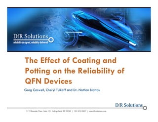
1) QFN packages have a higher susceptibility to failures caused by thermal cycling compared to other packages like QFP and BGA due to a higher CTE mismatch between the silicon die and substrate.
2) The use of conformal coatings and pottings can significantly reduce the thermal cycling lifetime of QFN packages. Conformal coatings can infiltrate under the package and induce lift during temperature cycling. Pottings with high CTE and modulus can cause warpage of the PCB and high stresses on solder joints.
3) For reliable use of coatings and pottings with QFNs, the mechanical properties like CTE, modulus and Tg must be carefully chosen to minimize stresses and warpage during
Thermo-Mechanical Simulation of Through Silicon Stack AssemblyKamal Karimanal
The electronics industry has been using Finite Element Analysis (FEA) to model IC package assembly process for understanding the effects of process conditions, material choice as well as design parameters. What was already practiced as an engineering-art within packaging organizations for monolithic IC packages has now become more complex due to the need for collaboration across organizational walls in the case of 3D stacking. The holistic solution needed for collaborative engineering of 3D stacking process calls for streamlined methodologies and information exchange protocols.
This presentation will introduce the idea of automated chip stacking process modeling approach with detailed discussions on inputs needed, gaps in existing modeling methodologies and output metrics of engineering relevance. The presentation will discuss wafer level warpage due to thinning and RDL films, their control, assembly implications of different under filling and encapsulation processes and pre attach warpage at reflow temperature
Package on-package interconnect for fan-out wafer level packagesInvensas
BVA® is a fine pitch vertical interconnect technology that forms package level 3D interconnects between active IC’s or passive devices, utilizing the existing wire bond infrastructure.
Ideal 3D Stacked Die Test - IEEE Semiconductor Wafer Test Workshop SWTW 2013Ira Feldman
My presentation from IEEE SWTW 2013 - For a full description please see my blog:
http://hightechbizdev.com/2013/06/10/ira-feldman-high-technology-business-development-ieee-semiconductor-wafer-test-workshop-2013/
The quad flat pack no lead or quad flat non-leaded (QFN) is one of the fastest growing package types in the electronics industry today. While the advantages of QFNs are well documented, concerns arise with its reliability and manufacturability. Acceptance of this package, especially in long-life, severe-environment, high-reliability applications, is currently limited. One of the most common drivers for reliability failures is inappropriate adoption of new technologies, such as the case with QFN. In this presentation, we will review and discuss QFN related reliability concerns and challenges, and propose Physics-of-Failure (PoF) based approaches to allow the confident introduction of QFN components into electronics products.
Optimized Local I/O ESD Protection for SerDes In Advanced SOI, BiCMOS and Fin...Sofics
Sofics presentation (B2.2) at the 1st International EOS/ESD Symposium on Design and System (IEDS). IEDS is dedicated to the fundamental understanding of issues related to electrostatic discharge on design and system and the application of this knowledge to the solution of problems.
Semiconductor companies are developing ever faster interfaces to satisfy the need for higher data throughputs. However, the parasitic capacitance of the traditional ESD solutions limits the signal frequency. This paper demonstrates low-cap Analog I/Os for high speed SerDes (28Gbps to 112Gbps) circuits created in advanced BiCMOS, SOI and FinFET nodes.
Intel Foveros and TSMC 3D SoIC are competing head-to-head for high-end packaging – How will Samsung react ?More information here : https://www.i-micronews.com/products/high-end-performance-packaging-3d-2-5d-integration-2020/
The 2010 State of supply chain performance study in Semiconductor industry was conducted with 52 companies with annual turnover exceeding USD 400 million.
The study was conducted from September to November 2010 by iCognitive consultants.
The Study used the same standard online questionnaire in all countries.
In addition, telephone interviews were carried out for verification of online results and additional qualitative data.
Advanced Packaging Role after Moore’s Law: Transition from Technology Node Er...Yole Developpement
The growing and diversifying system requirements have continued to drive the development of a variety of new package styles and configurations:
Small-form-factor
Lightweight technology
Low-profile technology
High-pin-count technology
High-speed technology
High Reliability
Improved thermal management
Lower cost
Fan-in WLP maintains its appeal as the package that can provide 2 unmatchable advantages:
• Reduced form factor
• Low cost
Demand is reaching available capacity
Technology innovation in fan-in WLP continues:
• Die size increases
• Bump pitch reduces
Foundry involvement is no longer a dent in fan-in WLP production
Increased activity of Chinese capital on the market
New applications are emerging while other are declining
• Disruptions also expected in the MEMS and CIS domains
• Internet of Things
Mobile sector is driving fan-in WLP production and growing
IoT is on the horizon and is expected to have a significant impact on fan-in packages and the packaging industry as a whole
GaN and SiC for power electronics applications 2015 Report by Yole DeveloppementYole Developpement
The SiC market is expected to treble and GaN is expected to explode - if challenges are overcome
In 2014, the SiC chip business was worth more than $133M. As in previous years, power factor correction (PFC) and photovoltaics (PV) are still the leading applications.
SiC diodes represent more than 80% of the market. In 2020, diodes will remain the main contributor across various applications, including electric and hybrid electric vehicles (EV/HEV), PV, PFC, wind, Uninterruptible Power Supplies (UPS) and motor drives.
SiC transistors will grow in parallel with diodes, driven by PV inverters. Challenges must be overcome prior to the adoption of pure SiC solutions for EV power train inverters, which is nevertheless expected by 2020.
Including the growth in both diodes and transistors we expect the total SiC market to more than treble by 2020, reaching $436M...
The Effect of Mixing BGA and Solder Paste Alloys on the Formation of VoidsAlpha
This presentation examines the drivers for mixed alloy systems, typical voiding requirements, common ways of reducing voids and the effects of mixed alloys on voiding.
The Effect of Coating and Potting on the Reliability of QFN DevicesCheryl Tulkoff
The lack of a compliant lead structure makes QFN devices more susceptible to PCB warpage related failures:
oMechanical properties of the potting material
oGlass transition temperature (Tg)
oModulus should be specified above and below the Tg
oCTE should be specified above and below the Tg
The design of the housing:
oMay provide a surface to which the potting material can pull against when shrinking causing PCB warpage
oShould be designed to provide as close to a hydrostatic pressure as possible (equal pressure on all sides)
Temperature Cycling and Fatigue in ElectronicsCheryl Tulkoff
The majority of electronic failures occur due to thermally induced stresses and strains caused by excessive differences in coefficients of thermal expansion (CTE) across materials.
CTE mismatches occur in both 1st and 2nd level interconnects in electronics assemblies.
-1st level interconnects connect the die to a substrate.
-This substrate can be underfilled so there are both global and local CTE mismatches to consider.
-2nd level interconnects connect the substrate, or package, to the printed circuit board (PCB). This would be considered a “board level” CTE mismatch.
-Several stress and strain mitigation techniques exist including the use of conformal coating.
The purpose of this presentation is to show that accelerated testing can be successfully used to predict solder joint and plated through hole (PTH) fatigue behavior.
Solving Problems with Reliability in the Lead-Free EraCheryl Tulkoff
This presentation provides a focused but comprehensive discussion on potential reliability issues that can arise within Pb-free processes. Areas of potential high risk are examined. For each reliability concern, a brief description is provided, followed by the current state of industry knowledge and an opportunity for risk mitigation based upon the product design, materials, complexity, volumes, and customer expectations of reliability. A final summary provides the attendees a roadmap for ensuring the reliability of Pb-free product.
In this paper the key property differences between solders and TLPS interconnect technologies are compared in detail for MLCC interconnects. The development of a new range of nickel Base Metal Electrode C0G MLCC stacks rated for 200oC is described and performance compared to traditional Precious Metal Electrode (PME) stacks. Thermal cycling performance to 200oC of BME X7R stacks made with 10Sn/88Pb/2Ag solders are compared to similar stacks made with TLPS interconnects of Cu-Sn and In-Ag. The development of leadless stacks, a new bulk capacitance form factor enabled by TLPS technology, is described and their properties compared to traditional stacks.
KEMET Webinar - Tantalum Polymer Surface Mount Capacitors New Industrial Appl...Ivana Ivanovska
Are you a designer looking for the last news in Industrial solutions? Based in industrial automation and miniaturization the Tantalum Polymer SMD T521 Series are key products offering better capacitance stability, better capacitance retention, lower ESR, higher ripple handling, and long life. The new product offering also allow miniaturization and high performance. In this presentation, the product features and electrical performance of new product offerings will be provided.
Today, multiple manufacturers have products rated at 230°C poised for market release. The tantalum anode, tantalum pentoxide dielectric and manganese dioxide primary cathode material stand up well to these temperatures, although some optimization of the design and manufacturing process for these materials have been required.
This Paper was Originally Presented at the High Temperature Electronics Network Conference on July, 2015
At PEIM 2016, KEMET presented work related to our BME C0G technology. This evaluation is driven by the rising need for a suitable Ceramic DC Link Capacitor for use in wide bandgap applications.
The presentation covers KEMET's previous application of BME C0G technology in similar areas.
Cristina talks about capacitors that can last longer at high temperatures are extreme humidity. In this case, when there is no moisture or too much moisture. This presentation covers the technology innovations applied to a high-reliability polymer tantalum capacitor.
Automotive Infotainment systems demand more from their components. Getting high performance parts found in smartphones with the quality expected of the automotive industry is a challenge.
KEMET's latest technology breakthrough with Low Voltage DC T591 Polymer Capacitors enables them to pass lifetime requirements targeted for Automotive applications.
Additionally there is a roadmap to getting to full AEC-Q200 qualifications with this same technology block.
This paper was presented by KEMET at the 2015 Applied Power Electronic Conference in Charlotte, NC.
KEMET Webinar - Update on ESA and military standard portfolioIvana Ivanovska
KEMET has successfully launched several High Reliability Tantalum Polymer SMD solutions to the market during the last years. The existing series T540/T541 based on the Mil 55365 specification and T583 ESCC3012/005 provide better capacitance stability, better capacitance retention, lower ESR, higher ripple handling, and long life combined with extreme requirements of Military, Defense and Aerospace applications. Leading the market and bringing innovation to these high demanding segments drive us to continuously expand our portfolio. We will up-date you on T580/T581 1st to market Military Polymer Standard and the T584 series, the ESA ultra-low ESR expansion.
Presentation on KEMET's Characterization of Transient Liquid Phase Sintering (TLPS) materials and their use in MLCCs. Presented on October 5, 2015, at the Material Science & Technology Conference in Columbus, OH by Dr John Bultitude.
KEMET Webinar - 0805 and 1206 footprints now available with higher rated volt...Markus Trautz
The "evergreen" application requirement for miniaturization has driven the development of small case size Polymer Capacitors to rated voltage levels of 25V now. In case sizes 0805 (4.7µF/25V) and 1206 (="A Case" footprint with max. height of 1.2 mm, 10µF/25V) customers can now benefit from the stable capacitance with DC voltage applied as well as the usage for application voltages up to 22.5V in case sizes usually known from Multi-Layer Ceramic Capacitors (MLCC´s).
With the MLCC technology undergoing changes towards even smaller case sizes and facing extended lead times, small case size Polymer Capacitors can represent an interesting alternative for your Capacitance requirement.
Water scarcity is the lack of fresh water resources to meet the standard water demand. There are two type of water scarcity. One is physical. The other is economic water scarcity.
Sachpazis:Terzaghi Bearing Capacity Estimation in simple terms with Calculati...Dr.Costas Sachpazis
Terzaghi's soil bearing capacity theory, developed by Karl Terzaghi, is a fundamental principle in geotechnical engineering used to determine the bearing capacity of shallow foundations. This theory provides a method to calculate the ultimate bearing capacity of soil, which is the maximum load per unit area that the soil can support without undergoing shear failure. The Calculation HTML Code included.
Cosmetic shop management system project report.pdfKamal Acharya
Buying new cosmetic products is difficult. It can even be scary for those who have sensitive skin and are prone to skin trouble. The information needed to alleviate this problem is on the back of each product, but it's thought to interpret those ingredient lists unless you have a background in chemistry.
Instead of buying and hoping for the best, we can use data science to help us predict which products may be good fits for us. It includes various function programs to do the above mentioned tasks.
Data file handling has been effectively used in the program.
The automated cosmetic shop management system should deal with the automation of general workflow and administration process of the shop. The main processes of the system focus on customer's request where the system is able to search the most appropriate products and deliver it to the customers. It should help the employees to quickly identify the list of cosmetic product that have reached the minimum quantity and also keep a track of expired date for each cosmetic product. It should help the employees to find the rack number in which the product is placed.It is also Faster and more efficient way.
Courier management system project report.pdfKamal Acharya
It is now-a-days very important for the people to send or receive articles like imported furniture, electronic items, gifts, business goods and the like. People depend vastly on different transport systems which mostly use the manual way of receiving and delivering the articles. There is no way to track the articles till they are received and there is no way to let the customer know what happened in transit, once he booked some articles. In such a situation, we need a system which completely computerizes the cargo activities including time to time tracking of the articles sent. This need is fulfilled by Courier Management System software which is online software for the cargo management people that enables them to receive the goods from a source and send them to a required destination and track their status from time to time.
COLLEGE BUS MANAGEMENT SYSTEM PROJECT REPORT.pdfKamal Acharya
The College Bus Management system is completely developed by Visual Basic .NET Version. The application is connect with most secured database language MS SQL Server. The application is develop by using best combination of front-end and back-end languages. The application is totally design like flat user interface. This flat user interface is more attractive user interface in 2017. The application is gives more important to the system functionality. The application is to manage the student’s details, driver’s details, bus details, bus route details, bus fees details and more. The application has only one unit for admin. The admin can manage the entire application. The admin can login into the application by using username and password of the admin. The application is develop for big and small colleges. It is more user friendly for non-computer person. Even they can easily learn how to manage the application within hours. The application is more secure by the admin. The system will give an effective output for the VB.Net and SQL Server given as input to the system. The compiled java program given as input to the system, after scanning the program will generate different reports. The application generates the report for users. The admin can view and download the report of the data. The application deliver the excel format reports. Because, excel formatted reports is very easy to understand the income and expense of the college bus. This application is mainly develop for windows operating system users. In 2017, 73% of people enterprises are using windows operating system. So the application will easily install for all the windows operating system users. The application-developed size is very low. The application consumes very low space in disk. Therefore, the user can allocate very minimum local disk space for this application.
About
Indigenized remote control interface card suitable for MAFI system CCR equipment. Compatible for IDM8000 CCR. Backplane mounted serial and TCP/Ethernet communication module for CCR remote access. IDM 8000 CCR remote control on serial and TCP protocol.
• Remote control: Parallel or serial interface.
• Compatible with MAFI CCR system.
• Compatible with IDM8000 CCR.
• Compatible with Backplane mount serial communication.
• Compatible with commercial and Defence aviation CCR system.
• Remote control system for accessing CCR and allied system over serial or TCP.
• Indigenized local Support/presence in India.
• Easy in configuration using DIP switches.
Technical Specifications
Indigenized remote control interface card suitable for MAFI system CCR equipment. Compatible for IDM8000 CCR. Backplane mounted serial and TCP/Ethernet communication module for CCR remote access. IDM 8000 CCR remote control on serial and TCP protocol.
Key Features
Indigenized remote control interface card suitable for MAFI system CCR equipment. Compatible for IDM8000 CCR. Backplane mounted serial and TCP/Ethernet communication module for CCR remote access. IDM 8000 CCR remote control on serial and TCP protocol.
• Remote control: Parallel or serial interface
• Compatible with MAFI CCR system
• Copatiable with IDM8000 CCR
• Compatible with Backplane mount serial communication.
• Compatible with commercial and Defence aviation CCR system.
• Remote control system for accessing CCR and allied system over serial or TCP.
• Indigenized local Support/presence in India.
Application
• Remote control: Parallel or serial interface.
• Compatible with MAFI CCR system.
• Compatible with IDM8000 CCR.
• Compatible with Backplane mount serial communication.
• Compatible with commercial and Defence aviation CCR system.
• Remote control system for accessing CCR and allied system over serial or TCP.
• Indigenized local Support/presence in India.
• Easy in configuration using DIP switches.