Downloaded 66 times
![Let’s get rid of pMOS
Reduced the capacitance and improved the delay
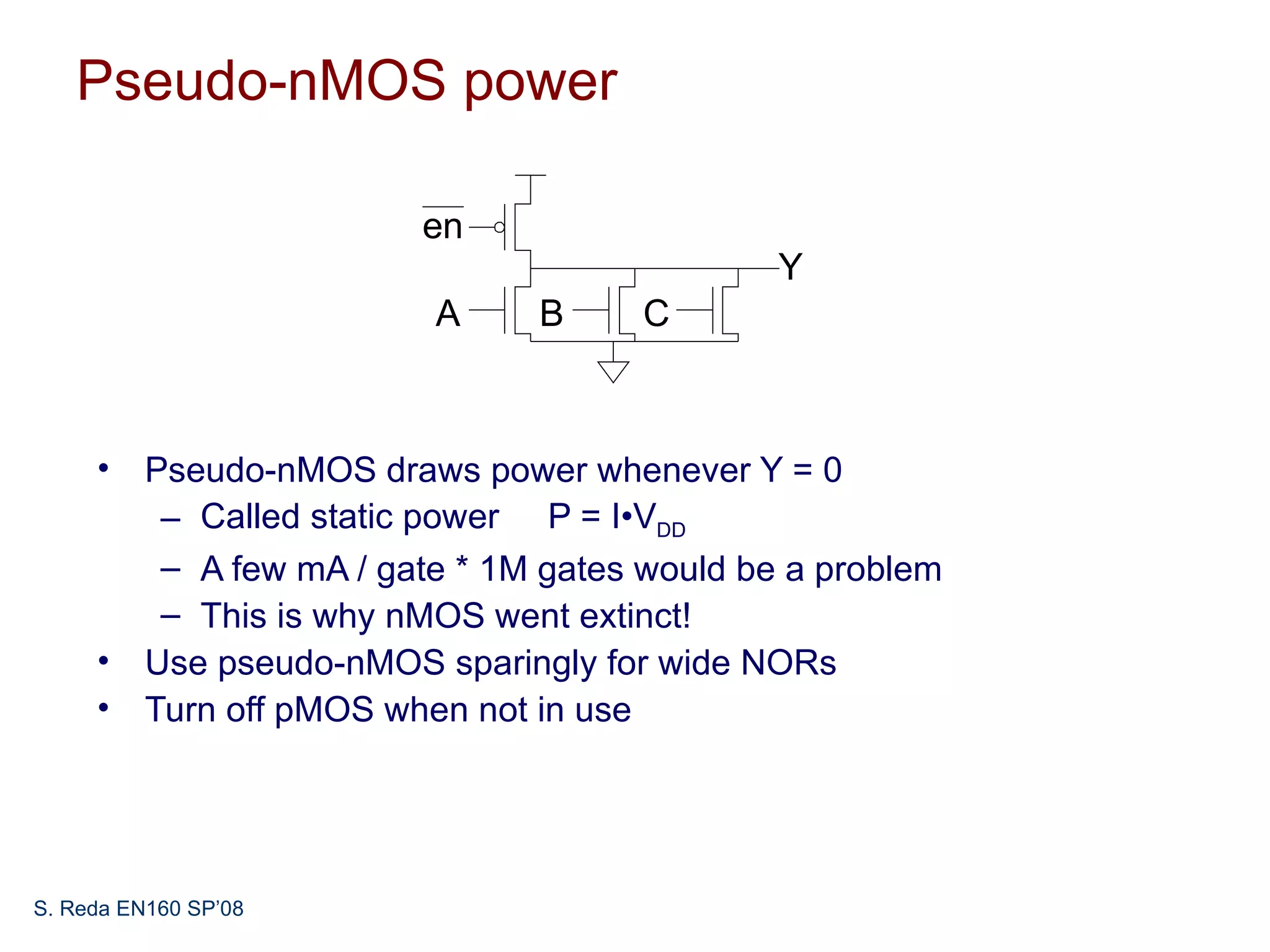
Increased static power consumption
Implementing a large resistive load in CMOS is not readily available
[see subsection 2.5.4]
S. Reda EN160 SP’08](https://image.slidesharecdn.com/lecture20-120613131842-phpapp01/75/Lecture20-2-2048.jpg)
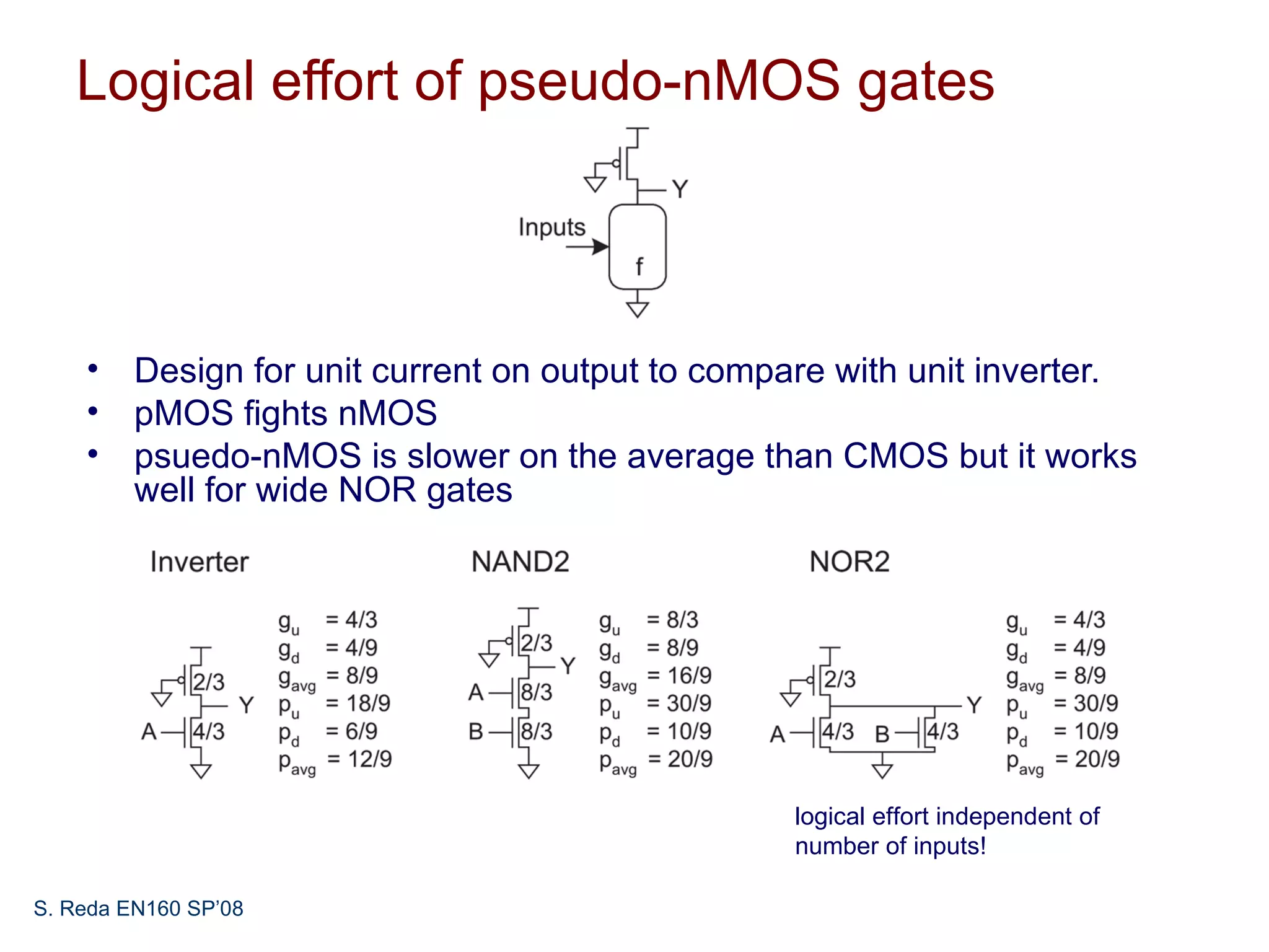
![2. Pseudo-nMOS circuits
• Use a pull-up transistor that is always ON
• Issues:
– Ratio or relative strength
– Make pMOS about ¼ effective strength of pulldown network
[see subsection 2.5.4]
S. Reda EN160 SP’08](https://image.slidesharecdn.com/lecture20-120613131842-phpapp01/75/Lecture20-3-2048.jpg)

![Possible solution: interface to a CMOS inverter
3.0
In
In
1.5µ m/0.25 µm Out
Voltage [V]
2.0
VD D x x
Out
0.5 µ m/0.25µ m
1.0
0.5µ m/0.25 µm
0.00 0.5 1 1.5 2
Time [ns]
Threshold voltage loss causes static power consumption
V DD
V DD
Level Restorer
Mr (AKA Lean Integration
B
M2 with Pass Transistors
A Mn
X
Out
- LEAP)
M1
A better design: full swing; reduces static power
S. Reda EN160 SP’08](https://image.slidesharecdn.com/lecture20-120613131842-phpapp01/75/Lecture20-10-2048.jpg)
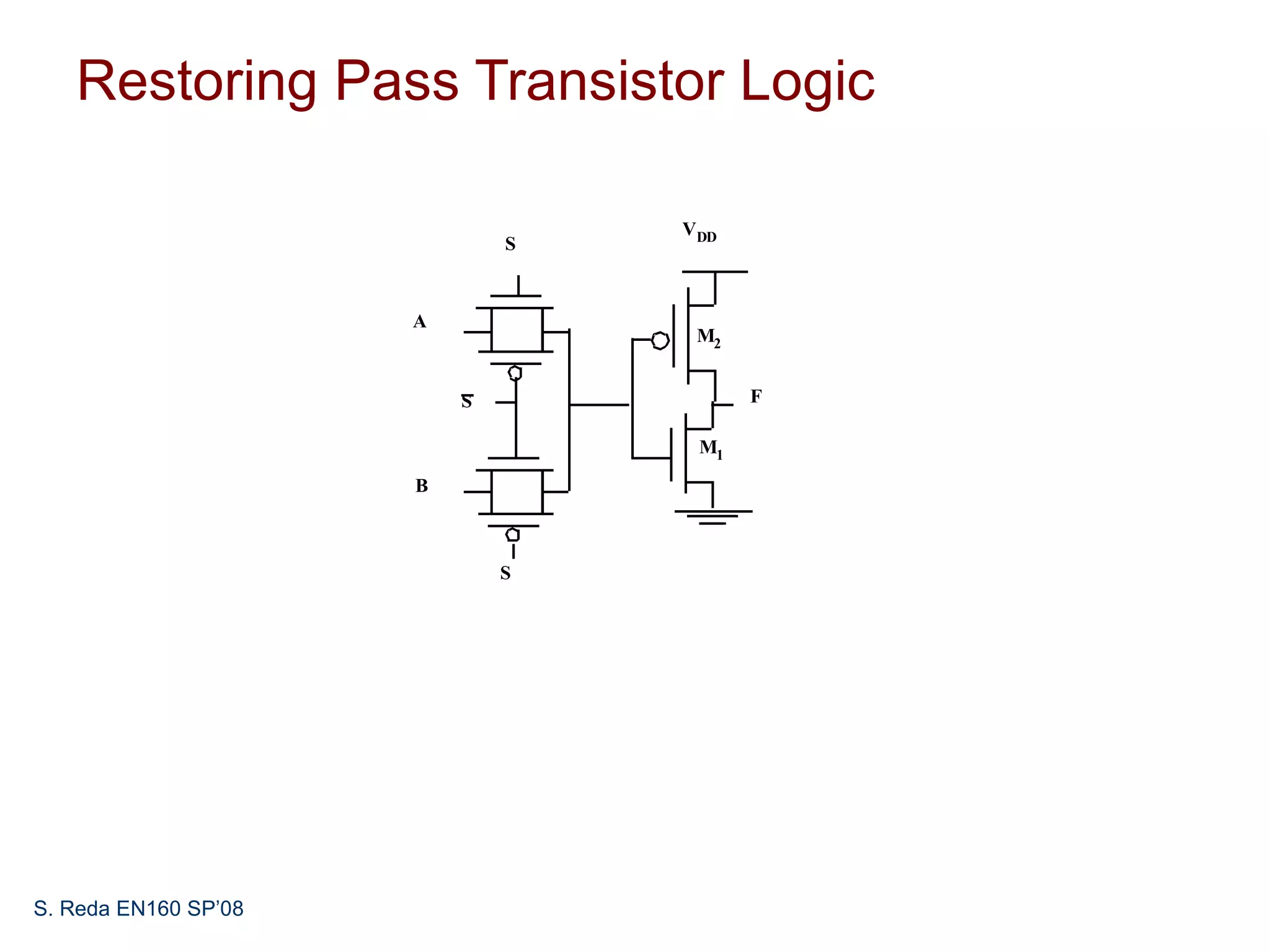

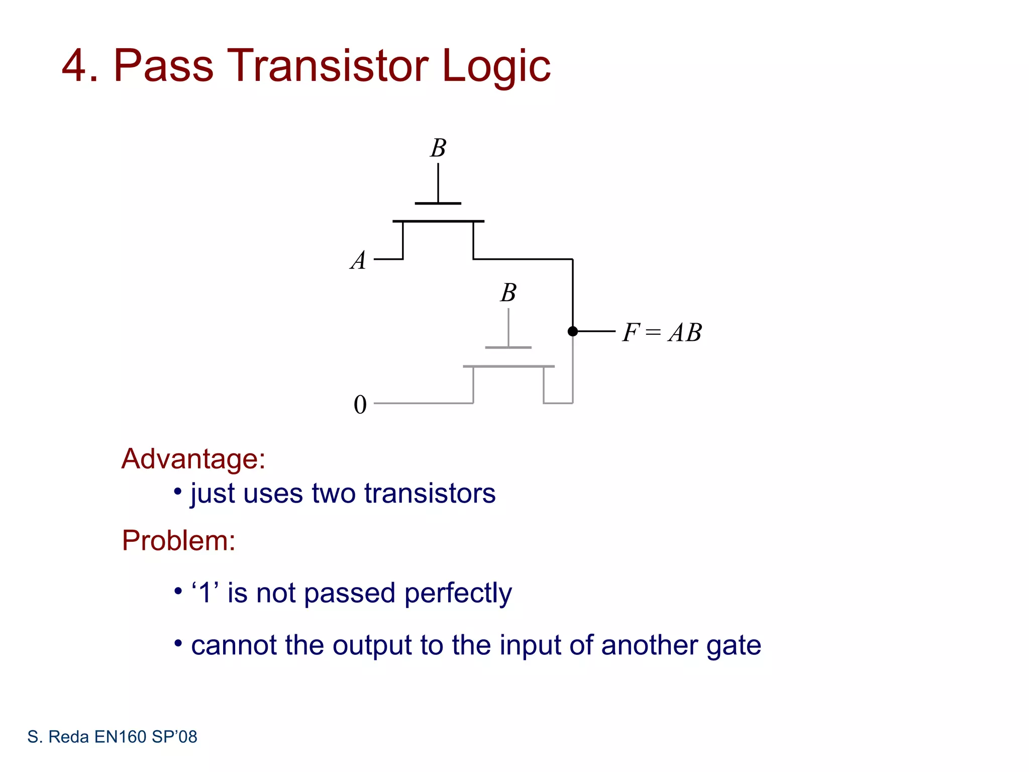
This document discusses different circuit design techniques for combinational logic, including: 1. Pseudo-nMOS circuits which use a permanently on pMOS transistor but have static power consumption issues. 2. Cascode Voltage Switch Logic seeks the performance of pseudo-nMOS without static power draw but requires input complements. 3. Pass transistor logic uses only two transistors but output levels are not restored perfectly and cannot drive other gates directly.