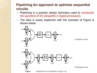
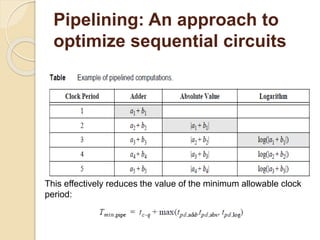
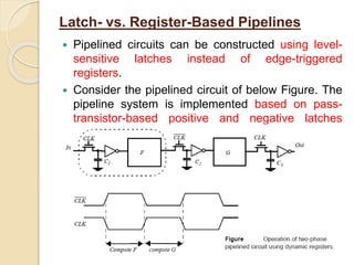
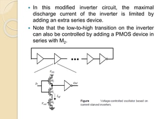
SlideShare a Scribd company logo
1 of 31
Pipelining Approach
D.Gopinath AP/ECE
Ramco Institute of technology
Academic year (2019-20 Even)
Pipelining An approach to optimize sequential
circuits
 Pipelining is a popular design technique used to accelerate
the operation of the datapaths in digital processors.
 The idea is easily explained with the example of Figure a
shown below.
Pipelining: An approach to optimize
sequential circuits
 The goal of the circuit is to compute log(|a - b|), where both a and b represent
streams of numbers, that is, the computation must be performed on a large set of
input values.
 The minimal clock period Tmin necessary to ensure correct evaluation is given as:
where tc-q and tsu are the propagation delay and the set-up time of the register,
respectively.
 We assume that the registers are edge-triggered D
registers.
 The term tpd,logic stands for the worst-case delay
path through the combinational network, which
consists of the adder, absolute value, and
logarithm functions.
 Assume that each logic module has an equal
propagation delay. We note that each logic module
is active for only 1/3 of the clock period (if the delay
of the register is ignored).
 For example, the adder unit is active during the first
third of the period and remains idle—this is, it does
no useful computation— during the other 2/3 of the
period.
 Pipelining is a technique to improve the resource
utilization, and increase the functional throughput.
 Assume that we introduce registers between the
logic blocks, as shown in above Figure b.
 This causes the computation for one set of input
data to spread over a number of clock periods, as
shown in below Table.
 The result for the data set (a1, b1) only appears at
the output after three clock-periods. At that time,
the circuit has already performed parts of the
computations for the next data
 sets, (a2, b2) and (a3,b3). The computation is
performed in an assembly-line fashion, hence the
name pipeline.
Pipelining: An approach to
optimize sequential circuits
This effectively reduces the value of the minimum allowable clock
period:
Latch- vs. Register-Based Pipelines
 Pipelined circuits can be constructed using level-
sensitive latches instead of edge-triggered
registers.
 Consider the pipelined circuit of below Figure. The
pipeline system is implemented based on pass-
transistor-based positive and negative latches
instead of edge triggered registers.
 A latch-based system gives significantly more
flexibility in implementing a pipelined system, and
often offers higher performance.
 When the clocks CLK and 𝐶𝐿𝐾 are non-
overlapping, correct pipeline operation is obtained.
Input data is sampled on C1 at the negative edge of
CLK and the computation of logic block F starts;
the result of the logic block F is stored on C2 on the
falling edge of 𝐶𝐿𝐾, and the computation of logic
block G starts.
 The non-overlapping of the clocks ensures correct
operation. The value stored on C2 at the end of the
CLK low phase is the result of passing the previous
input (stored on the falling edge of CLK on C1)
through the logic function F.
 When overlap exists between CLK and 𝐶𝐿𝐾, the
next input is already being applied to F, and its
effect might propagate to C2 before 𝐶𝐿𝐾 goes low
 In other words, a race develops between the
previous input and the current one. Which value
wins depends upon the logic function F, the overlap
time, and the value of the inputs
NORA-CMOS—A Logic Style for Pipelined
Structures
 The latch-based pipeline circuit can also be
implemented using C2MOS latches, as shown in
below Figure.
 The operation is similar to the one discussed
above. This topology has one additional, important
property:
 A C2MOS-based pipelined circuit is race-free as
long as all the logic functions F (implemented
using static logic) between the latches are non-
inverting.
NORA-CMOS—A Logic Style for Pipelined
Structures
 The reasoning for the above argument is similar to
the argument made in the construction of a C2MOS
register. During a (0-0) overlap between CLK and
𝐶𝐿𝐾, all C2MOS latches, simplify to pure pull-up
networks (see in C2MOS register Figure).
 The only way a signal can race from stage to stage
under this condition is when the logic function F is
inverting, as illustrated in below Figure, where F is
replaced by a single, static CMOS inverter.
NORA-CMOS—A Logic Style for Pipelined
Structures
 Based on this concept, a logic circuit style called
NORA-CMOS was conceived.
 It combines C2MOS pipeline registers and NORA
dynamic logic function blocks.
 Each module consists of a block of combinational
logic that can be a mixture of static and dynamic
logic, followed by a C2MOS latch.
 Logic and latch are clocked in such a way that both
are simultaneously in either evaluation, or hold
(precharge) mode. A block that is in evaluation
during CLK = 1 is called a CLK-module, while the
inverse is called a 𝐶𝐿𝐾-module.
Design Rules
In order to ensure correct operation, two important rules
should always be followed:
The dynamic-logic rule: Inputs to a dynamic CLKn
(CLKp) block are only allowed to make a single 0 to 1 (1
to 0) transition during the evaluation period.
The C2MOS rule: In order to avoid races, the number of
static inversions between C2MOS latches should be
even.
 Consider the situation pictured in below Figure a.
During precharge (CLK = 0), the output register of the
module has to be in hold mode, isolating the output
node from the internal events in the module.
 Assume now that a (0-0) overlap occurs. Node A gets
precharged to VDD, while the latch simplifies to a pull-up
network (Figure b). It can be observed that under those
circumstances the output node charges to VDD, and the
stored value is erased!
 This malfunctioning is caused by the fact that the
number of static inversions between the last dynamic
node in the module and the latch is odd, which creates
an active path between the precharged node and the
output.
 This translates into the following rule:
 The number of static inversions between the last
dynamic block in a logic function and the C2MOS latch
should be even. This and similar considerations lead to
a reformulated C2MOS rule
Revised C2MOS Rule
 The number of static inversions between C2MOS
latches should be even (in the absence of dynamic
nodes); if dynamic nodes are present, the number
of static inverters between a latch and a dynamic
gate in the logic block should be even. The number
of static inversions between the last dynamic gate
in a logic block and the latch should be even as
well.
Non-Bistable Sequential
Circuits
 Other regenerative circuits can be catalogued as
astable and monostable.
 The astable circuit act as oscillators and can, for
instance, be used for on-chip clock generation.
 The monostable circuit serve as pulse
generators, also called one-shot circuits.
 Another interesting regenerative circuit is the
Schmitt trigger. This component has the useful
property of showing hysteresis in its dc
characteristics—its switching threshold is variable
and depends upon the direction of the transition
(low-to-high or high-to-low).
The Schmitt Trigger
A Schmitt trigger is a device with two
important properties:
 It responds to a slowly changing input waveform
with a fast transition time at the output.
 The voltage-transfer characteristic of the device
displays different switching thresholds for positive-
and negative-going input signals.
 This is demonstrated in below Figure, where a
typical voltage-transfer characteristic of the Schmitt
trigger is shown (and its schematics symbol). The
switching thresholds for the low-to-high and high to
low transitions are called VM+ and VM-, respectively.
The hysteresis voltage is defined as the difference
between the two.
 One of the main uses of the Schmitt trigger is to
turn a noisy or slowly varying input signal into a
clean digital output signal. This is illustrated in
below Figure.
CMOS Implementation of Schmitt trigger
The idea behind this circuit is that the switching
threshold of a CMOS inverter is determined by the
(kn/kp) ratio between the NMOS and PMOS transistors.
Increasing the ratio results in a reduction of the
threshold, while decreasing it results in an increase in
VM.
 Suppose that Vin is initially equal to 0, so that Vout =
0 as well. The feedback loop biases the PMOS
transistor M4 in the conductive mode while M3 is
off.
 The input signal effectively connects to an inverter
consisting of two PMOS transistors in parallel (M2
and M4) as a pull-up network, and a single NMOS
transistor (M1) in the pull-down chain.
 This modifies the effective transistor ratio of the
inverter to kM1/(kM2+kM4), which moves the
switching threshold upwards.
 Similar behavior
Monostable Sequential
Circuits
 A monostable element is a circuit that generates a pulse
of a predetermined width every time the quiescent
circuit is triggered by a pulse or transition event. It is
called monostable because it has only one stable state
(the quiescent one).
 A trigger event, which is either a signal transition or a
pulse, causes the circuit to go temporarily into another
quasi-stable state. This means that it eventually returns
to its original state after a time period determined by the
circuit parameters.
 This circuit, also called a one-shot, is useful in
generating pulses of a known length. This functionality
is required in a wide range of applications.
 We have already seen the use of a one-shot in the
construction of glitch registers.
Astable Circuits
 An astable circuit has no stable states. The output
oscillates back and forth between two quasi-stable
states with a period determined by the circuit
topology and parameters (delay, power supply,
etc.).
 One of the main applications of oscillators is the
on-chip generation of clock signals.
 The ring oscillator is a simple, example of an
astable circuit.
 It consists of an odd number of inverters connected
in a circular chain. Due to the odd number of
inversions, no stable operation point exists, and the
circuit oscillates with a period equal to 2xtpxN, with
N the number of inverters in the chain and tp the
propagation delay of each inverter.
Ring oscillator
 The ring oscillator composed of cascaded inverters
produces a waveform with a fixed oscillating frequency
determined by the delay of an inverter in the CMOS
process.
 In many applications, it is necessary to control the
frequency of the oscillator. An example of such a circuit
is the voltage-controlled oscillator (VCO), whose
oscillation frequency is a function of a control voltage.
 The standard ring oscillator can be modified into a VCO
by replacing the standard inverter with a current-
starved inverter as shown in below Figure.
 The mechanism for controlling the delay of each inverter
is to limit the current available to discharge the load
capacitance of the gate.
 In this modified inverter circuit, the maximal
discharge current of the inverter is limited by
adding an extra series device.
 Note that the low-to-high transition on the inverter
can also be controlled by adding a PMOS device in
series with M2.
 The added NMOS transistor M3, is controlled by an
analog control voltage Vcntl, which determines the
available discharge current. Lowering Vcntl reduces
the discharge current and, hence, increases tpHL.
 The ability to alter the propagation delay per stage
allows us to control the frequency of the ring
structure.
TEXT BOOKS:
 Neil H.E. Weste, David Money Harris “CMOS VLSI
Design: A Circuits and Systems Perspective”, 4th
Edition, Pearson, 2017 (UNIT I,II,V).
 Jan M. Rabaey, Anantha Chandrakasan, Borivoje.
Nikolic, “Digital Integrated Circuits:A Design
perspective”, Second Edition , Pearson , 2016.(UNIT
III,IV)
REFERENCES
 M.J. Smith, “Application Specific Integrated Circuits”,
Addisson Wesley, 1997.
 Sung-Mo kang, Yusuf leblebici, Chulwoo Kim “CMOS
Digital Integrated Circuits:Analysis & Design”,4th edition
McGraw Hill Education,2013.
 Wayne Wolf, “Modern VLSI Design: System On Chip”,
Pearson Education, 2007.
 R.Jacob Baker, Harry W.LI, David E.Boyee, “CMOS
Circuit Design, Layout and Simulation”, Prentice Hall of
India 2005.
THANK YOU

More Related Content

What's hot

Pass Transistor Logic
Pass Transistor LogicPass Transistor Logic
Pass Transistor LogicDiwaker Pant
 
Phase Locked Loop (PLL)
Phase Locked Loop (PLL)Phase Locked Loop (PLL)
Phase Locked Loop (PLL)Debayon Saha
 
Coherent and Non-coherent detection of ASK, FSK AND QASK
Coherent and Non-coherent detection of ASK, FSK AND QASKCoherent and Non-coherent detection of ASK, FSK AND QASK
Coherent and Non-coherent detection of ASK, FSK AND QASKnaimish12
 
Smart traffic light controller using verilog
Smart traffic light controller using verilogSmart traffic light controller using verilog
Smart traffic light controller using verilogVaishaliVaishali14
 
Power dissipation cmos
Power dissipation cmosPower dissipation cmos
Power dissipation cmosRajesh Tiwary
 
UNIT-III-DIGITAL SYSTEM DESIGN
UNIT-III-DIGITAL SYSTEM DESIGNUNIT-III-DIGITAL SYSTEM DESIGN
UNIT-III-DIGITAL SYSTEM DESIGNDr.YNM
 
Orthogonal Frequency Division Multiplexing (OFDM)
Orthogonal Frequency Division Multiplexing (OFDM)Orthogonal Frequency Division Multiplexing (OFDM)
Orthogonal Frequency Division Multiplexing (OFDM)Gagan Randhawa
 
Fpga architectures and applications
Fpga architectures and applicationsFpga architectures and applications
Fpga architectures and applicationsSudhanshu Janwadkar
 
Driving large capacitive loads
Driving large capacitive loadsDriving large capacitive loads
Driving large capacitive loadsRavi Selvaraj
 
3.2 modulation formats bpsk, qpsk, oqpsk,
3.2 modulation formats   bpsk, qpsk, oqpsk,3.2 modulation formats   bpsk, qpsk, oqpsk,
3.2 modulation formats bpsk, qpsk, oqpsk,JAIGANESH SEKAR
 
fpga programming
fpga programmingfpga programming
fpga programmingAnish Gupta
 
Two cavity klystron
Two cavity klystronTwo cavity klystron
Two cavity klystronabhikalmegh
 
Sequential cmos logic circuits
Sequential cmos logic circuitsSequential cmos logic circuits
Sequential cmos logic circuitsSakshi Bhargava
 
Microwave oscillator design
Microwave oscillator designMicrowave oscillator design
Microwave oscillator designImane Haf
 
Design for testability and automatic test pattern generation
Design for testability and automatic test pattern generationDesign for testability and automatic test pattern generation
Design for testability and automatic test pattern generationDilip Mathuria
 

What's hot (20)

Pass Transistor Logic
Pass Transistor LogicPass Transistor Logic
Pass Transistor Logic
 
Sampling Theorem
Sampling TheoremSampling Theorem
Sampling Theorem
 
Phase Locked Loop (PLL)
Phase Locked Loop (PLL)Phase Locked Loop (PLL)
Phase Locked Loop (PLL)
 
Coherent and Non-coherent detection of ASK, FSK AND QASK
Coherent and Non-coherent detection of ASK, FSK AND QASKCoherent and Non-coherent detection of ASK, FSK AND QASK
Coherent and Non-coherent detection of ASK, FSK AND QASK
 
Smart traffic light controller using verilog
Smart traffic light controller using verilogSmart traffic light controller using verilog
Smart traffic light controller using verilog
 
Power dissipation cmos
Power dissipation cmosPower dissipation cmos
Power dissipation cmos
 
UNIT-III-DIGITAL SYSTEM DESIGN
UNIT-III-DIGITAL SYSTEM DESIGNUNIT-III-DIGITAL SYSTEM DESIGN
UNIT-III-DIGITAL SYSTEM DESIGN
 
Orthogonal Frequency Division Multiplexing (OFDM)
Orthogonal Frequency Division Multiplexing (OFDM)Orthogonal Frequency Division Multiplexing (OFDM)
Orthogonal Frequency Division Multiplexing (OFDM)
 
Dynamic logic circuits
Dynamic logic circuitsDynamic logic circuits
Dynamic logic circuits
 
Fpga architectures and applications
Fpga architectures and applicationsFpga architectures and applications
Fpga architectures and applications
 
Driving large capacitive loads
Driving large capacitive loadsDriving large capacitive loads
Driving large capacitive loads
 
3.2 modulation formats bpsk, qpsk, oqpsk,
3.2 modulation formats   bpsk, qpsk, oqpsk,3.2 modulation formats   bpsk, qpsk, oqpsk,
3.2 modulation formats bpsk, qpsk, oqpsk,
 
fpga programming
fpga programmingfpga programming
fpga programming
 
Two cavity klystron
Two cavity klystronTwo cavity klystron
Two cavity klystron
 
Sequential cmos logic circuits
Sequential cmos logic circuitsSequential cmos logic circuits
Sequential cmos logic circuits
 
Pass Transistor Logic
Pass Transistor LogicPass Transistor Logic
Pass Transistor Logic
 
Microwave oscillator design
Microwave oscillator designMicrowave oscillator design
Microwave oscillator design
 
Combinational Logic
Combinational LogicCombinational Logic
Combinational Logic
 
Design for testability and automatic test pattern generation
Design for testability and automatic test pattern generationDesign for testability and automatic test pattern generation
Design for testability and automatic test pattern generation
 
test generation
test generationtest generation
test generation
 

Similar to Pipelining approach

Design of Counter Using SRAM
Design of Counter Using SRAMDesign of Counter Using SRAM
Design of Counter Using SRAMIOSRJECE
 
Iaetsd an mtcmos technique for optimizing low
Iaetsd an mtcmos technique for optimizing lowIaetsd an mtcmos technique for optimizing low
Iaetsd an mtcmos technique for optimizing lowIaetsd Iaetsd
 
Double tail comparator
Double tail comparatorDouble tail comparator
Double tail comparatorMdLogic Mdls
 
A Novel Flipflop Topology for High Speed and Area Efficient Logic Structure D...
A Novel Flipflop Topology for High Speed and Area Efficient Logic Structure D...A Novel Flipflop Topology for High Speed and Area Efficient Logic Structure D...
A Novel Flipflop Topology for High Speed and Area Efficient Logic Structure D...IOSR Journals
 
Design of Low Voltage D-Flip Flop Using MOS Current Mode Logic (MCML) For Hig...
Design of Low Voltage D-Flip Flop Using MOS Current Mode Logic (MCML) For Hig...Design of Low Voltage D-Flip Flop Using MOS Current Mode Logic (MCML) For Hig...
Design of Low Voltage D-Flip Flop Using MOS Current Mode Logic (MCML) For Hig...IOSRJVSP
 
A Simulation Based Analysis of Lowering Dynamic Power in a CMOS Inverter
A Simulation Based Analysis of Lowering Dynamic Power in a CMOS InverterA Simulation Based Analysis of Lowering Dynamic Power in a CMOS Inverter
A Simulation Based Analysis of Lowering Dynamic Power in a CMOS Inverteridescitation
 
Analysis and design_of_a_low-voltage_low-power[1]
Analysis and design_of_a_low-voltage_low-power[1]Analysis and design_of_a_low-voltage_low-power[1]
Analysis and design_of_a_low-voltage_low-power[1]Srinivas Naidu
 
Design of an ADC using High Precision Comparator with Time Domain Offset Canc...
Design of an ADC using High Precision Comparator with Time Domain Offset Canc...Design of an ADC using High Precision Comparator with Time Domain Offset Canc...
Design of an ADC using High Precision Comparator with Time Domain Offset Canc...IJTET Journal
 
High Speed and Low Pedestal Error Bootstrapped CMOS Sample and Hold Circuit
High Speed and Low Pedestal Error Bootstrapped CMOS Sample and Hold CircuitHigh Speed and Low Pedestal Error Bootstrapped CMOS Sample and Hold Circuit
High Speed and Low Pedestal Error Bootstrapped CMOS Sample and Hold CircuitIJECEIAES
 
A Sub Threshold Source Coupled Logic Based Design of Low Power CMOS Analog Mu...
A Sub Threshold Source Coupled Logic Based Design of Low Power CMOS Analog Mu...A Sub Threshold Source Coupled Logic Based Design of Low Power CMOS Analog Mu...
A Sub Threshold Source Coupled Logic Based Design of Low Power CMOS Analog Mu...VLSICS Design
 
vlsi 2 unit.pdfvlsi unit 2 important notes for ece department
vlsi 2 unit.pdfvlsi unit 2 important notes for ece departmentvlsi 2 unit.pdfvlsi unit 2 important notes for ece department
vlsi 2 unit.pdfvlsi unit 2 important notes for ece departmentnitcse
 
Compact low power high slew-rate cmos buffer amplifier with power gating tech...
Compact low power high slew-rate cmos buffer amplifier with power gating tech...Compact low power high slew-rate cmos buffer amplifier with power gating tech...
Compact low power high slew-rate cmos buffer amplifier with power gating tech...VLSICS Design
 
A Novel Multi Port Dc/Dc Converter Topology Using Zero Voltage Switching For...
A Novel Multi Port Dc/Dc Converter Topology Using Zero  Voltage Switching For...A Novel Multi Port Dc/Dc Converter Topology Using Zero  Voltage Switching For...
A Novel Multi Port Dc/Dc Converter Topology Using Zero Voltage Switching For...IJMER
 
International Journal of Engineering Research and Development
International Journal of Engineering Research and DevelopmentInternational Journal of Engineering Research and Development
International Journal of Engineering Research and DevelopmentIJERD Editor
 
A New Single-Stage Multilevel Type Full-Bridge Converter Applied to closed lo...
A New Single-Stage Multilevel Type Full-Bridge Converter Applied to closed lo...A New Single-Stage Multilevel Type Full-Bridge Converter Applied to closed lo...
A New Single-Stage Multilevel Type Full-Bridge Converter Applied to closed lo...IOSR Journals
 
Energy Efficient Design of Multiplexer Using Adiabatic logic
Energy Efficient Design of Multiplexer Using Adiabatic logicEnergy Efficient Design of Multiplexer Using Adiabatic logic
Energy Efficient Design of Multiplexer Using Adiabatic logicIJEEE
 

Similar to Pipelining approach (20)

Design of Counter Using SRAM
Design of Counter Using SRAMDesign of Counter Using SRAM
Design of Counter Using SRAM
 
Iaetsd an mtcmos technique for optimizing low
Iaetsd an mtcmos technique for optimizing lowIaetsd an mtcmos technique for optimizing low
Iaetsd an mtcmos technique for optimizing low
 
Double tail comparator
Double tail comparatorDouble tail comparator
Double tail comparator
 
A Novel Flipflop Topology for High Speed and Area Efficient Logic Structure D...
A Novel Flipflop Topology for High Speed and Area Efficient Logic Structure D...A Novel Flipflop Topology for High Speed and Area Efficient Logic Structure D...
A Novel Flipflop Topology for High Speed and Area Efficient Logic Structure D...
 
A Novel Flipflop Topology for High Speed and Area Efficient Logic Structure D...
A Novel Flipflop Topology for High Speed and Area Efficient Logic Structure D...A Novel Flipflop Topology for High Speed and Area Efficient Logic Structure D...
A Novel Flipflop Topology for High Speed and Area Efficient Logic Structure D...
 
15 47-58
15 47-5815 47-58
15 47-58
 
Design of Low Voltage D-Flip Flop Using MOS Current Mode Logic (MCML) For Hig...
Design of Low Voltage D-Flip Flop Using MOS Current Mode Logic (MCML) For Hig...Design of Low Voltage D-Flip Flop Using MOS Current Mode Logic (MCML) For Hig...
Design of Low Voltage D-Flip Flop Using MOS Current Mode Logic (MCML) For Hig...
 
A Simulation Based Analysis of Lowering Dynamic Power in a CMOS Inverter
A Simulation Based Analysis of Lowering Dynamic Power in a CMOS InverterA Simulation Based Analysis of Lowering Dynamic Power in a CMOS Inverter
A Simulation Based Analysis of Lowering Dynamic Power in a CMOS Inverter
 
Analysis and design_of_a_low-voltage_low-power[1]
Analysis and design_of_a_low-voltage_low-power[1]Analysis and design_of_a_low-voltage_low-power[1]
Analysis and design_of_a_low-voltage_low-power[1]
 
Design of an ADC using High Precision Comparator with Time Domain Offset Canc...
Design of an ADC using High Precision Comparator with Time Domain Offset Canc...Design of an ADC using High Precision Comparator with Time Domain Offset Canc...
Design of an ADC using High Precision Comparator with Time Domain Offset Canc...
 
High Speed and Low Pedestal Error Bootstrapped CMOS Sample and Hold Circuit
High Speed and Low Pedestal Error Bootstrapped CMOS Sample and Hold CircuitHigh Speed and Low Pedestal Error Bootstrapped CMOS Sample and Hold Circuit
High Speed and Low Pedestal Error Bootstrapped CMOS Sample and Hold Circuit
 
A Sub Threshold Source Coupled Logic Based Design of Low Power CMOS Analog Mu...
A Sub Threshold Source Coupled Logic Based Design of Low Power CMOS Analog Mu...A Sub Threshold Source Coupled Logic Based Design of Low Power CMOS Analog Mu...
A Sub Threshold Source Coupled Logic Based Design of Low Power CMOS Analog Mu...
 
vlsi 2 unit.pdfvlsi unit 2 important notes for ece department
vlsi 2 unit.pdfvlsi unit 2 important notes for ece departmentvlsi 2 unit.pdfvlsi unit 2 important notes for ece department
vlsi 2 unit.pdfvlsi unit 2 important notes for ece department
 
Compact low power high slew-rate cmos buffer amplifier with power gating tech...
Compact low power high slew-rate cmos buffer amplifier with power gating tech...Compact low power high slew-rate cmos buffer amplifier with power gating tech...
Compact low power high slew-rate cmos buffer amplifier with power gating tech...
 
ha_report modified
ha_report  modifiedha_report  modified
ha_report modified
 
H010335563
H010335563H010335563
H010335563
 
A Novel Multi Port Dc/Dc Converter Topology Using Zero Voltage Switching For...
A Novel Multi Port Dc/Dc Converter Topology Using Zero  Voltage Switching For...A Novel Multi Port Dc/Dc Converter Topology Using Zero  Voltage Switching For...
A Novel Multi Port Dc/Dc Converter Topology Using Zero Voltage Switching For...
 
International Journal of Engineering Research and Development
International Journal of Engineering Research and DevelopmentInternational Journal of Engineering Research and Development
International Journal of Engineering Research and Development
 
A New Single-Stage Multilevel Type Full-Bridge Converter Applied to closed lo...
A New Single-Stage Multilevel Type Full-Bridge Converter Applied to closed lo...A New Single-Stage Multilevel Type Full-Bridge Converter Applied to closed lo...
A New Single-Stage Multilevel Type Full-Bridge Converter Applied to closed lo...
 
Energy Efficient Design of Multiplexer Using Adiabatic logic
Energy Efficient Design of Multiplexer Using Adiabatic logicEnergy Efficient Design of Multiplexer Using Adiabatic logic
Energy Efficient Design of Multiplexer Using Adiabatic logic
 

More from GopinathD17

Aperture Antennas.pptx
Aperture Antennas.pptxAperture Antennas.pptx
Aperture Antennas.pptxGopinathD17
 
Digital Electronics-ppt.pptx
Digital Electronics-ppt.pptxDigital Electronics-ppt.pptx
Digital Electronics-ppt.pptxGopinathD17
 
Interrupt, DMA controller.pptx
Interrupt, DMA controller.pptxInterrupt, DMA controller.pptx
Interrupt, DMA controller.pptxGopinathD17
 
Aperture antennas
Aperture antennasAperture antennas
Aperture antennasGopinathD17
 
COMBINATIONAL CIRCUITS
COMBINATIONAL CIRCUITSCOMBINATIONAL CIRCUITS
COMBINATIONAL CIRCUITSGopinathD17
 
Transmission lines and RF systems
Transmission lines and RF systemsTransmission lines and RF systems
Transmission lines and RF systemsGopinathD17
 
Intra and inter emi, elements of interference
Intra and inter emi, elements of interferenceIntra and inter emi, elements of interference
Intra and inter emi, elements of interferenceGopinathD17
 
Different types of interconnection of two port networks
Different types of interconnection  of  two  port  networksDifferent types of interconnection  of  two  port  networks
Different types of interconnection of two port networksGopinathD17
 
EQUATION OF CONTINUITY AND KIRCHHOFF'S CURRENT LAW
EQUATION OF CONTINUITY AND KIRCHHOFF'S CURRENT LAWEQUATION OF CONTINUITY AND KIRCHHOFF'S CURRENT LAW
EQUATION OF CONTINUITY AND KIRCHHOFF'S CURRENT LAWGopinathD17
 
EMI MITIGATION TECHNIQUES
EMI MITIGATION TECHNIQUESEMI MITIGATION TECHNIQUES
EMI MITIGATION TECHNIQUESGopinathD17
 
Applications of maxwell's equation to the rectangular waveguide
Applications of maxwell's equation to the rectangular waveguideApplications of maxwell's equation to the rectangular waveguide
Applications of maxwell's equation to the rectangular waveguideGopinathD17
 
Code Division Multiple Access
Code Division Multiple AccessCode Division Multiple Access
Code Division Multiple AccessGopinathD17
 
Spiral and log periodic antenna
Spiral and log periodic antennaSpiral and log periodic antenna
Spiral and log periodic antennaGopinathD17
 
Semiconductor junction device
Semiconductor junction deviceSemiconductor junction device
Semiconductor junction deviceGopinathD17
 
General theory of transmission lines
General theory of transmission linesGeneral theory of transmission lines
General theory of transmission linesGopinathD17
 

More from GopinathD17 (15)

Aperture Antennas.pptx
Aperture Antennas.pptxAperture Antennas.pptx
Aperture Antennas.pptx
 
Digital Electronics-ppt.pptx
Digital Electronics-ppt.pptxDigital Electronics-ppt.pptx
Digital Electronics-ppt.pptx
 
Interrupt, DMA controller.pptx
Interrupt, DMA controller.pptxInterrupt, DMA controller.pptx
Interrupt, DMA controller.pptx
 
Aperture antennas
Aperture antennasAperture antennas
Aperture antennas
 
COMBINATIONAL CIRCUITS
COMBINATIONAL CIRCUITSCOMBINATIONAL CIRCUITS
COMBINATIONAL CIRCUITS
 
Transmission lines and RF systems
Transmission lines and RF systemsTransmission lines and RF systems
Transmission lines and RF systems
 
Intra and inter emi, elements of interference
Intra and inter emi, elements of interferenceIntra and inter emi, elements of interference
Intra and inter emi, elements of interference
 
Different types of interconnection of two port networks
Different types of interconnection  of  two  port  networksDifferent types of interconnection  of  two  port  networks
Different types of interconnection of two port networks
 
EQUATION OF CONTINUITY AND KIRCHHOFF'S CURRENT LAW
EQUATION OF CONTINUITY AND KIRCHHOFF'S CURRENT LAWEQUATION OF CONTINUITY AND KIRCHHOFF'S CURRENT LAW
EQUATION OF CONTINUITY AND KIRCHHOFF'S CURRENT LAW
 
EMI MITIGATION TECHNIQUES
EMI MITIGATION TECHNIQUESEMI MITIGATION TECHNIQUES
EMI MITIGATION TECHNIQUES
 
Applications of maxwell's equation to the rectangular waveguide
Applications of maxwell's equation to the rectangular waveguideApplications of maxwell's equation to the rectangular waveguide
Applications of maxwell's equation to the rectangular waveguide
 
Code Division Multiple Access
Code Division Multiple AccessCode Division Multiple Access
Code Division Multiple Access
 
Spiral and log periodic antenna
Spiral and log periodic antennaSpiral and log periodic antenna
Spiral and log periodic antenna
 
Semiconductor junction device
Semiconductor junction deviceSemiconductor junction device
Semiconductor junction device
 
General theory of transmission lines
General theory of transmission linesGeneral theory of transmission lines
General theory of transmission lines
 

Recently uploaded

Work-Permit-Receiver-in-Saudi-Aramco.pptx
Work-Permit-Receiver-in-Saudi-Aramco.pptxWork-Permit-Receiver-in-Saudi-Aramco.pptx
Work-Permit-Receiver-in-Saudi-Aramco.pptxJuliansyahHarahap1
 
Hostel management system project report..pdf
Hostel management system project report..pdfHostel management system project report..pdf
Hostel management system project report..pdfKamal Acharya
 
457503602-5-Gas-Well-Testing-and-Analysis-pptx.pptx
457503602-5-Gas-Well-Testing-and-Analysis-pptx.pptx457503602-5-Gas-Well-Testing-and-Analysis-pptx.pptx
457503602-5-Gas-Well-Testing-and-Analysis-pptx.pptxrouholahahmadi9876
 
Thermal Engineering -unit - III & IV.ppt
Thermal Engineering -unit - III & IV.pptThermal Engineering -unit - III & IV.ppt
Thermal Engineering -unit - III & IV.pptDineshKumar4165
 
scipt v1.pptxcxxxxxxxxxxxxxxxxxxxxxxxxxxxxxxxxxxxxxxxxxxxxxxxxxxxxxxxxxxxxxxx...
scipt v1.pptxcxxxxxxxxxxxxxxxxxxxxxxxxxxxxxxxxxxxxxxxxxxxxxxxxxxxxxxxxxxxxxxx...scipt v1.pptxcxxxxxxxxxxxxxxxxxxxxxxxxxxxxxxxxxxxxxxxxxxxxxxxxxxxxxxxxxxxxxxx...
scipt v1.pptxcxxxxxxxxxxxxxxxxxxxxxxxxxxxxxxxxxxxxxxxxxxxxxxxxxxxxxxxxxxxxxxx...HenryBriggs2
 
Moment Distribution Method For Btech Civil
Moment Distribution Method For Btech CivilMoment Distribution Method For Btech Civil
Moment Distribution Method For Btech CivilVinayVitekari
 
School management system project Report.pdf
School management system project Report.pdfSchool management system project Report.pdf
School management system project Report.pdfKamal Acharya
 
Thermal Engineering-R & A / C - unit - V
Thermal Engineering-R & A / C - unit - VThermal Engineering-R & A / C - unit - V
Thermal Engineering-R & A / C - unit - VDineshKumar4165
 
DeepFakes presentation : brief idea of DeepFakes
DeepFakes presentation : brief idea of DeepFakesDeepFakes presentation : brief idea of DeepFakes
DeepFakes presentation : brief idea of DeepFakesMayuraD1
 
DC MACHINE-Motoring and generation, Armature circuit equation
DC MACHINE-Motoring and generation, Armature circuit equationDC MACHINE-Motoring and generation, Armature circuit equation
DC MACHINE-Motoring and generation, Armature circuit equationBhangaleSonal
 
💚Trustworthy Call Girls Pune Call Girls Service Just Call 🍑👄6378878445 🍑👄 Top...
💚Trustworthy Call Girls Pune Call Girls Service Just Call 🍑👄6378878445 🍑👄 Top...💚Trustworthy Call Girls Pune Call Girls Service Just Call 🍑👄6378878445 🍑👄 Top...
💚Trustworthy Call Girls Pune Call Girls Service Just Call 🍑👄6378878445 🍑👄 Top...vershagrag
 
Online food ordering system project report.pdf
Online food ordering system project report.pdfOnline food ordering system project report.pdf
Online food ordering system project report.pdfKamal Acharya
 
NO1 Top No1 Amil Baba In Azad Kashmir, Kashmir Black Magic Specialist Expert ...
NO1 Top No1 Amil Baba In Azad Kashmir, Kashmir Black Magic Specialist Expert ...NO1 Top No1 Amil Baba In Azad Kashmir, Kashmir Black Magic Specialist Expert ...
NO1 Top No1 Amil Baba In Azad Kashmir, Kashmir Black Magic Specialist Expert ...Amil baba
 
Unit 4_Part 1 CSE2001 Exception Handling and Function Template and Class Temp...
Unit 4_Part 1 CSE2001 Exception Handling and Function Template and Class Temp...Unit 4_Part 1 CSE2001 Exception Handling and Function Template and Class Temp...
Unit 4_Part 1 CSE2001 Exception Handling and Function Template and Class Temp...drmkjayanthikannan
 
Double Revolving field theory-how the rotor develops torque
Double Revolving field theory-how the rotor develops torqueDouble Revolving field theory-how the rotor develops torque
Double Revolving field theory-how the rotor develops torqueBhangaleSonal
 
AIRCANVAS[1].pdf mini project for btech students
AIRCANVAS[1].pdf mini project for btech studentsAIRCANVAS[1].pdf mini project for btech students
AIRCANVAS[1].pdf mini project for btech studentsvanyagupta248
 
Digital Communication Essentials: DPCM, DM, and ADM .pptx
Digital Communication Essentials: DPCM, DM, and ADM .pptxDigital Communication Essentials: DPCM, DM, and ADM .pptx
Digital Communication Essentials: DPCM, DM, and ADM .pptxpritamlangde
 
Learn the concepts of Thermodynamics on Magic Marks
Learn the concepts of Thermodynamics on Magic MarksLearn the concepts of Thermodynamics on Magic Marks
Learn the concepts of Thermodynamics on Magic MarksMagic Marks
 
Orlando’s Arnold Palmer Hospital Layout Strategy-1.pptx
Orlando’s Arnold Palmer Hospital Layout Strategy-1.pptxOrlando’s Arnold Palmer Hospital Layout Strategy-1.pptx
Orlando’s Arnold Palmer Hospital Layout Strategy-1.pptxMuhammadAsimMuhammad6
 

Recently uploaded (20)

Work-Permit-Receiver-in-Saudi-Aramco.pptx
Work-Permit-Receiver-in-Saudi-Aramco.pptxWork-Permit-Receiver-in-Saudi-Aramco.pptx
Work-Permit-Receiver-in-Saudi-Aramco.pptx
 
Hostel management system project report..pdf
Hostel management system project report..pdfHostel management system project report..pdf
Hostel management system project report..pdf
 
457503602-5-Gas-Well-Testing-and-Analysis-pptx.pptx
457503602-5-Gas-Well-Testing-and-Analysis-pptx.pptx457503602-5-Gas-Well-Testing-and-Analysis-pptx.pptx
457503602-5-Gas-Well-Testing-and-Analysis-pptx.pptx
 
Thermal Engineering -unit - III & IV.ppt
Thermal Engineering -unit - III & IV.pptThermal Engineering -unit - III & IV.ppt
Thermal Engineering -unit - III & IV.ppt
 
scipt v1.pptxcxxxxxxxxxxxxxxxxxxxxxxxxxxxxxxxxxxxxxxxxxxxxxxxxxxxxxxxxxxxxxxx...
scipt v1.pptxcxxxxxxxxxxxxxxxxxxxxxxxxxxxxxxxxxxxxxxxxxxxxxxxxxxxxxxxxxxxxxxx...scipt v1.pptxcxxxxxxxxxxxxxxxxxxxxxxxxxxxxxxxxxxxxxxxxxxxxxxxxxxxxxxxxxxxxxxx...
scipt v1.pptxcxxxxxxxxxxxxxxxxxxxxxxxxxxxxxxxxxxxxxxxxxxxxxxxxxxxxxxxxxxxxxxx...
 
Moment Distribution Method For Btech Civil
Moment Distribution Method For Btech CivilMoment Distribution Method For Btech Civil
Moment Distribution Method For Btech Civil
 
School management system project Report.pdf
School management system project Report.pdfSchool management system project Report.pdf
School management system project Report.pdf
 
Thermal Engineering-R & A / C - unit - V
Thermal Engineering-R & A / C - unit - VThermal Engineering-R & A / C - unit - V
Thermal Engineering-R & A / C - unit - V
 
DeepFakes presentation : brief idea of DeepFakes
DeepFakes presentation : brief idea of DeepFakesDeepFakes presentation : brief idea of DeepFakes
DeepFakes presentation : brief idea of DeepFakes
 
Integrated Test Rig For HTFE-25 - Neometrix
Integrated Test Rig For HTFE-25 - NeometrixIntegrated Test Rig For HTFE-25 - Neometrix
Integrated Test Rig For HTFE-25 - Neometrix
 
DC MACHINE-Motoring and generation, Armature circuit equation
DC MACHINE-Motoring and generation, Armature circuit equationDC MACHINE-Motoring and generation, Armature circuit equation
DC MACHINE-Motoring and generation, Armature circuit equation
 
💚Trustworthy Call Girls Pune Call Girls Service Just Call 🍑👄6378878445 🍑👄 Top...
💚Trustworthy Call Girls Pune Call Girls Service Just Call 🍑👄6378878445 🍑👄 Top...💚Trustworthy Call Girls Pune Call Girls Service Just Call 🍑👄6378878445 🍑👄 Top...
💚Trustworthy Call Girls Pune Call Girls Service Just Call 🍑👄6378878445 🍑👄 Top...
 
Online food ordering system project report.pdf
Online food ordering system project report.pdfOnline food ordering system project report.pdf
Online food ordering system project report.pdf
 
NO1 Top No1 Amil Baba In Azad Kashmir, Kashmir Black Magic Specialist Expert ...
NO1 Top No1 Amil Baba In Azad Kashmir, Kashmir Black Magic Specialist Expert ...NO1 Top No1 Amil Baba In Azad Kashmir, Kashmir Black Magic Specialist Expert ...
NO1 Top No1 Amil Baba In Azad Kashmir, Kashmir Black Magic Specialist Expert ...
 
Unit 4_Part 1 CSE2001 Exception Handling and Function Template and Class Temp...
Unit 4_Part 1 CSE2001 Exception Handling and Function Template and Class Temp...Unit 4_Part 1 CSE2001 Exception Handling and Function Template and Class Temp...
Unit 4_Part 1 CSE2001 Exception Handling and Function Template and Class Temp...
 
Double Revolving field theory-how the rotor develops torque
Double Revolving field theory-how the rotor develops torqueDouble Revolving field theory-how the rotor develops torque
Double Revolving field theory-how the rotor develops torque
 
AIRCANVAS[1].pdf mini project for btech students
AIRCANVAS[1].pdf mini project for btech studentsAIRCANVAS[1].pdf mini project for btech students
AIRCANVAS[1].pdf mini project for btech students
 
Digital Communication Essentials: DPCM, DM, and ADM .pptx
Digital Communication Essentials: DPCM, DM, and ADM .pptxDigital Communication Essentials: DPCM, DM, and ADM .pptx
Digital Communication Essentials: DPCM, DM, and ADM .pptx
 
Learn the concepts of Thermodynamics on Magic Marks
Learn the concepts of Thermodynamics on Magic MarksLearn the concepts of Thermodynamics on Magic Marks
Learn the concepts of Thermodynamics on Magic Marks
 
Orlando’s Arnold Palmer Hospital Layout Strategy-1.pptx
Orlando’s Arnold Palmer Hospital Layout Strategy-1.pptxOrlando’s Arnold Palmer Hospital Layout Strategy-1.pptx
Orlando’s Arnold Palmer Hospital Layout Strategy-1.pptx
 

Pipelining approach

  • 1. Pipelining Approach D.Gopinath AP/ECE Ramco Institute of technology Academic year (2019-20 Even)
  • 2. Pipelining An approach to optimize sequential circuits  Pipelining is a popular design technique used to accelerate the operation of the datapaths in digital processors.  The idea is easily explained with the example of Figure a shown below.
  • 3. Pipelining: An approach to optimize sequential circuits  The goal of the circuit is to compute log(|a - b|), where both a and b represent streams of numbers, that is, the computation must be performed on a large set of input values.  The minimal clock period Tmin necessary to ensure correct evaluation is given as: where tc-q and tsu are the propagation delay and the set-up time of the register, respectively.
  • 4.  We assume that the registers are edge-triggered D registers.  The term tpd,logic stands for the worst-case delay path through the combinational network, which consists of the adder, absolute value, and logarithm functions.  Assume that each logic module has an equal propagation delay. We note that each logic module is active for only 1/3 of the clock period (if the delay of the register is ignored).  For example, the adder unit is active during the first third of the period and remains idle—this is, it does no useful computation— during the other 2/3 of the period.
  • 5.  Pipelining is a technique to improve the resource utilization, and increase the functional throughput.  Assume that we introduce registers between the logic blocks, as shown in above Figure b.  This causes the computation for one set of input data to spread over a number of clock periods, as shown in below Table.  The result for the data set (a1, b1) only appears at the output after three clock-periods. At that time, the circuit has already performed parts of the computations for the next data  sets, (a2, b2) and (a3,b3). The computation is performed in an assembly-line fashion, hence the name pipeline.
  • 6. Pipelining: An approach to optimize sequential circuits This effectively reduces the value of the minimum allowable clock period:
  • 7. Latch- vs. Register-Based Pipelines  Pipelined circuits can be constructed using level- sensitive latches instead of edge-triggered registers.  Consider the pipelined circuit of below Figure. The pipeline system is implemented based on pass- transistor-based positive and negative latches instead of edge triggered registers.
  • 8.  A latch-based system gives significantly more flexibility in implementing a pipelined system, and often offers higher performance.  When the clocks CLK and 𝐶𝐿𝐾 are non- overlapping, correct pipeline operation is obtained. Input data is sampled on C1 at the negative edge of CLK and the computation of logic block F starts; the result of the logic block F is stored on C2 on the falling edge of 𝐶𝐿𝐾, and the computation of logic block G starts.  The non-overlapping of the clocks ensures correct operation. The value stored on C2 at the end of the CLK low phase is the result of passing the previous input (stored on the falling edge of CLK on C1) through the logic function F.
  • 9.  When overlap exists between CLK and 𝐶𝐿𝐾, the next input is already being applied to F, and its effect might propagate to C2 before 𝐶𝐿𝐾 goes low  In other words, a race develops between the previous input and the current one. Which value wins depends upon the logic function F, the overlap time, and the value of the inputs
  • 10. NORA-CMOS—A Logic Style for Pipelined Structures  The latch-based pipeline circuit can also be implemented using C2MOS latches, as shown in below Figure.
  • 11.  The operation is similar to the one discussed above. This topology has one additional, important property:  A C2MOS-based pipelined circuit is race-free as long as all the logic functions F (implemented using static logic) between the latches are non- inverting. NORA-CMOS—A Logic Style for Pipelined Structures
  • 12.  The reasoning for the above argument is similar to the argument made in the construction of a C2MOS register. During a (0-0) overlap between CLK and 𝐶𝐿𝐾, all C2MOS latches, simplify to pure pull-up networks (see in C2MOS register Figure).  The only way a signal can race from stage to stage under this condition is when the logic function F is inverting, as illustrated in below Figure, where F is replaced by a single, static CMOS inverter.
  • 13. NORA-CMOS—A Logic Style for Pipelined Structures  Based on this concept, a logic circuit style called NORA-CMOS was conceived.  It combines C2MOS pipeline registers and NORA dynamic logic function blocks.  Each module consists of a block of combinational logic that can be a mixture of static and dynamic logic, followed by a C2MOS latch.  Logic and latch are clocked in such a way that both are simultaneously in either evaluation, or hold (precharge) mode. A block that is in evaluation during CLK = 1 is called a CLK-module, while the inverse is called a 𝐶𝐿𝐾-module.
  • 14.
  • 15. Design Rules In order to ensure correct operation, two important rules should always be followed: The dynamic-logic rule: Inputs to a dynamic CLKn (CLKp) block are only allowed to make a single 0 to 1 (1 to 0) transition during the evaluation period. The C2MOS rule: In order to avoid races, the number of static inversions between C2MOS latches should be even.
  • 16.  Consider the situation pictured in below Figure a. During precharge (CLK = 0), the output register of the module has to be in hold mode, isolating the output node from the internal events in the module.  Assume now that a (0-0) overlap occurs. Node A gets precharged to VDD, while the latch simplifies to a pull-up network (Figure b). It can be observed that under those circumstances the output node charges to VDD, and the stored value is erased!  This malfunctioning is caused by the fact that the number of static inversions between the last dynamic node in the module and the latch is odd, which creates an active path between the precharged node and the output.  This translates into the following rule:  The number of static inversions between the last dynamic block in a logic function and the C2MOS latch should be even. This and similar considerations lead to a reformulated C2MOS rule
  • 17.
  • 18. Revised C2MOS Rule  The number of static inversions between C2MOS latches should be even (in the absence of dynamic nodes); if dynamic nodes are present, the number of static inverters between a latch and a dynamic gate in the logic block should be even. The number of static inversions between the last dynamic gate in a logic block and the latch should be even as well.
  • 19. Non-Bistable Sequential Circuits  Other regenerative circuits can be catalogued as astable and monostable.  The astable circuit act as oscillators and can, for instance, be used for on-chip clock generation.  The monostable circuit serve as pulse generators, also called one-shot circuits.  Another interesting regenerative circuit is the Schmitt trigger. This component has the useful property of showing hysteresis in its dc characteristics—its switching threshold is variable and depends upon the direction of the transition (low-to-high or high-to-low).
  • 20. The Schmitt Trigger A Schmitt trigger is a device with two important properties:  It responds to a slowly changing input waveform with a fast transition time at the output.  The voltage-transfer characteristic of the device displays different switching thresholds for positive- and negative-going input signals.
  • 21.  This is demonstrated in below Figure, where a typical voltage-transfer characteristic of the Schmitt trigger is shown (and its schematics symbol). The switching thresholds for the low-to-high and high to low transitions are called VM+ and VM-, respectively. The hysteresis voltage is defined as the difference between the two.
  • 22.  One of the main uses of the Schmitt trigger is to turn a noisy or slowly varying input signal into a clean digital output signal. This is illustrated in below Figure.
  • 23. CMOS Implementation of Schmitt trigger The idea behind this circuit is that the switching threshold of a CMOS inverter is determined by the (kn/kp) ratio between the NMOS and PMOS transistors. Increasing the ratio results in a reduction of the threshold, while decreasing it results in an increase in VM.
  • 24.  Suppose that Vin is initially equal to 0, so that Vout = 0 as well. The feedback loop biases the PMOS transistor M4 in the conductive mode while M3 is off.  The input signal effectively connects to an inverter consisting of two PMOS transistors in parallel (M2 and M4) as a pull-up network, and a single NMOS transistor (M1) in the pull-down chain.  This modifies the effective transistor ratio of the inverter to kM1/(kM2+kM4), which moves the switching threshold upwards.  Similar behavior
  • 25. Monostable Sequential Circuits  A monostable element is a circuit that generates a pulse of a predetermined width every time the quiescent circuit is triggered by a pulse or transition event. It is called monostable because it has only one stable state (the quiescent one).  A trigger event, which is either a signal transition or a pulse, causes the circuit to go temporarily into another quasi-stable state. This means that it eventually returns to its original state after a time period determined by the circuit parameters.  This circuit, also called a one-shot, is useful in generating pulses of a known length. This functionality is required in a wide range of applications.  We have already seen the use of a one-shot in the construction of glitch registers.
  • 26. Astable Circuits  An astable circuit has no stable states. The output oscillates back and forth between two quasi-stable states with a period determined by the circuit topology and parameters (delay, power supply, etc.).  One of the main applications of oscillators is the on-chip generation of clock signals.  The ring oscillator is a simple, example of an astable circuit.  It consists of an odd number of inverters connected in a circular chain. Due to the odd number of inversions, no stable operation point exists, and the circuit oscillates with a period equal to 2xtpxN, with N the number of inverters in the chain and tp the propagation delay of each inverter.
  • 27. Ring oscillator  The ring oscillator composed of cascaded inverters produces a waveform with a fixed oscillating frequency determined by the delay of an inverter in the CMOS process.  In many applications, it is necessary to control the frequency of the oscillator. An example of such a circuit is the voltage-controlled oscillator (VCO), whose oscillation frequency is a function of a control voltage.  The standard ring oscillator can be modified into a VCO by replacing the standard inverter with a current- starved inverter as shown in below Figure.  The mechanism for controlling the delay of each inverter is to limit the current available to discharge the load capacitance of the gate.
  • 28.  In this modified inverter circuit, the maximal discharge current of the inverter is limited by adding an extra series device.  Note that the low-to-high transition on the inverter can also be controlled by adding a PMOS device in series with M2.
  • 29.  The added NMOS transistor M3, is controlled by an analog control voltage Vcntl, which determines the available discharge current. Lowering Vcntl reduces the discharge current and, hence, increases tpHL.  The ability to alter the propagation delay per stage allows us to control the frequency of the ring structure.
  • 30. TEXT BOOKS:  Neil H.E. Weste, David Money Harris “CMOS VLSI Design: A Circuits and Systems Perspective”, 4th Edition, Pearson, 2017 (UNIT I,II,V).  Jan M. Rabaey, Anantha Chandrakasan, Borivoje. Nikolic, “Digital Integrated Circuits:A Design perspective”, Second Edition , Pearson , 2016.(UNIT III,IV) REFERENCES  M.J. Smith, “Application Specific Integrated Circuits”, Addisson Wesley, 1997.  Sung-Mo kang, Yusuf leblebici, Chulwoo Kim “CMOS Digital Integrated Circuits:Analysis & Design”,4th edition McGraw Hill Education,2013.  Wayne Wolf, “Modern VLSI Design: System On Chip”, Pearson Education, 2007.  R.Jacob Baker, Harry W.LI, David E.Boyee, “CMOS Circuit Design, Layout and Simulation”, Prentice Hall of India 2005.