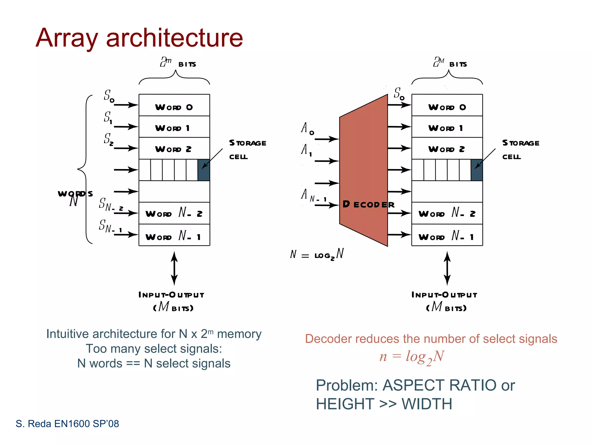
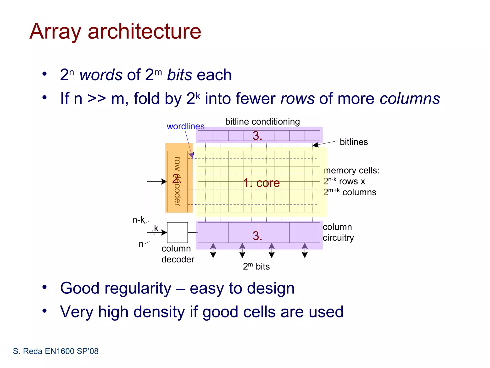
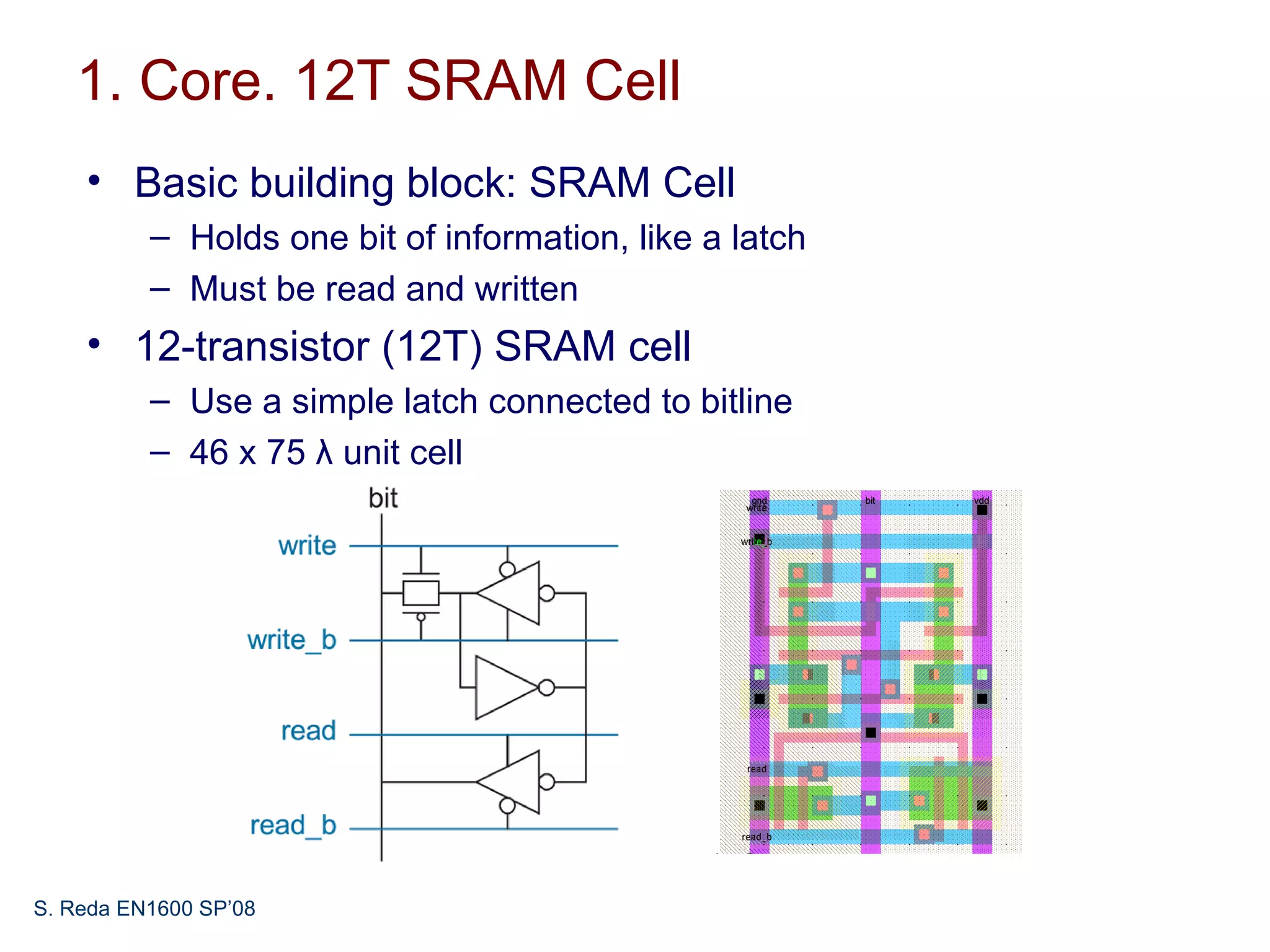
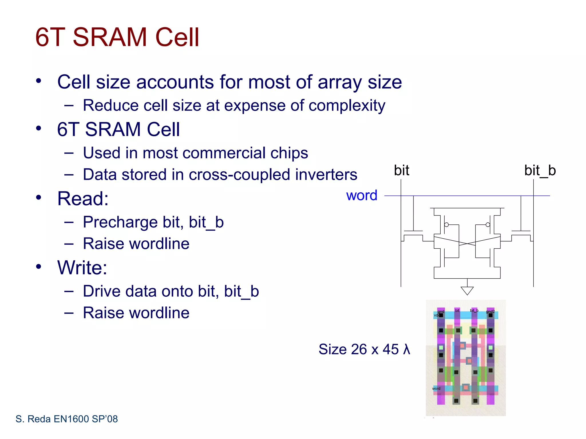
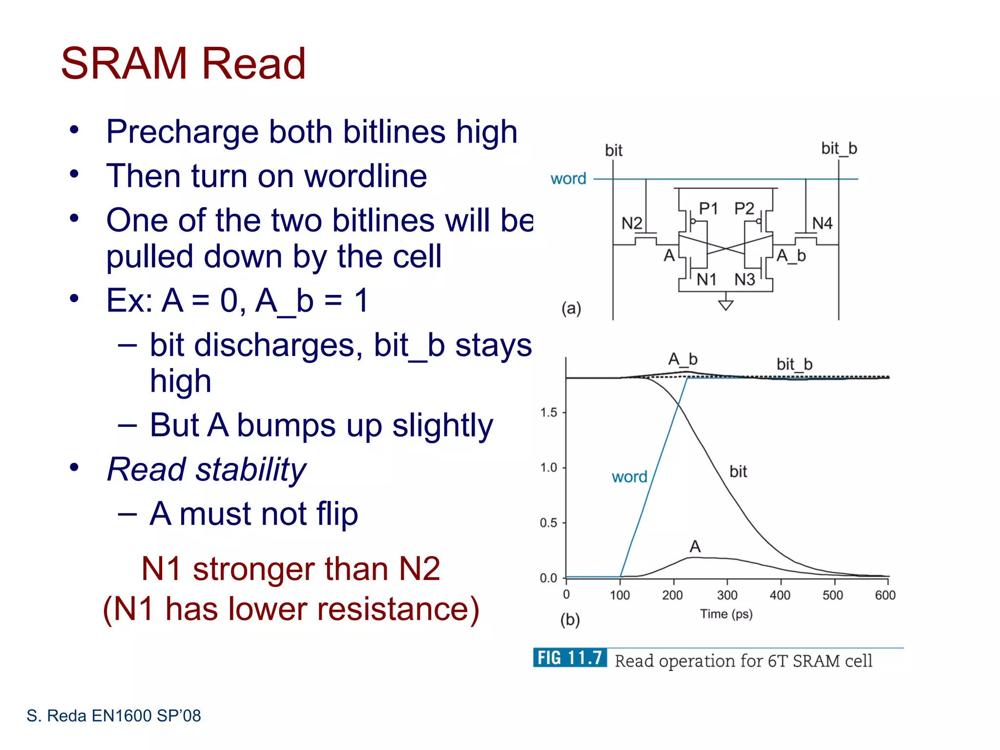
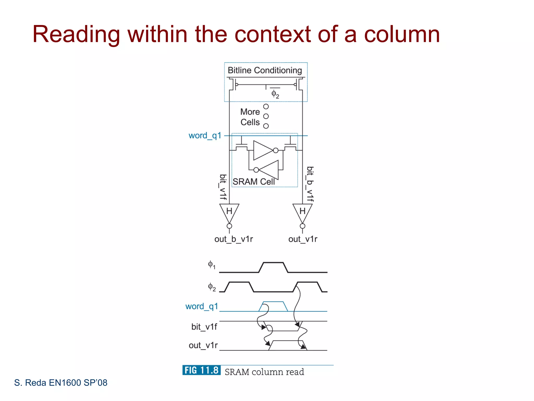
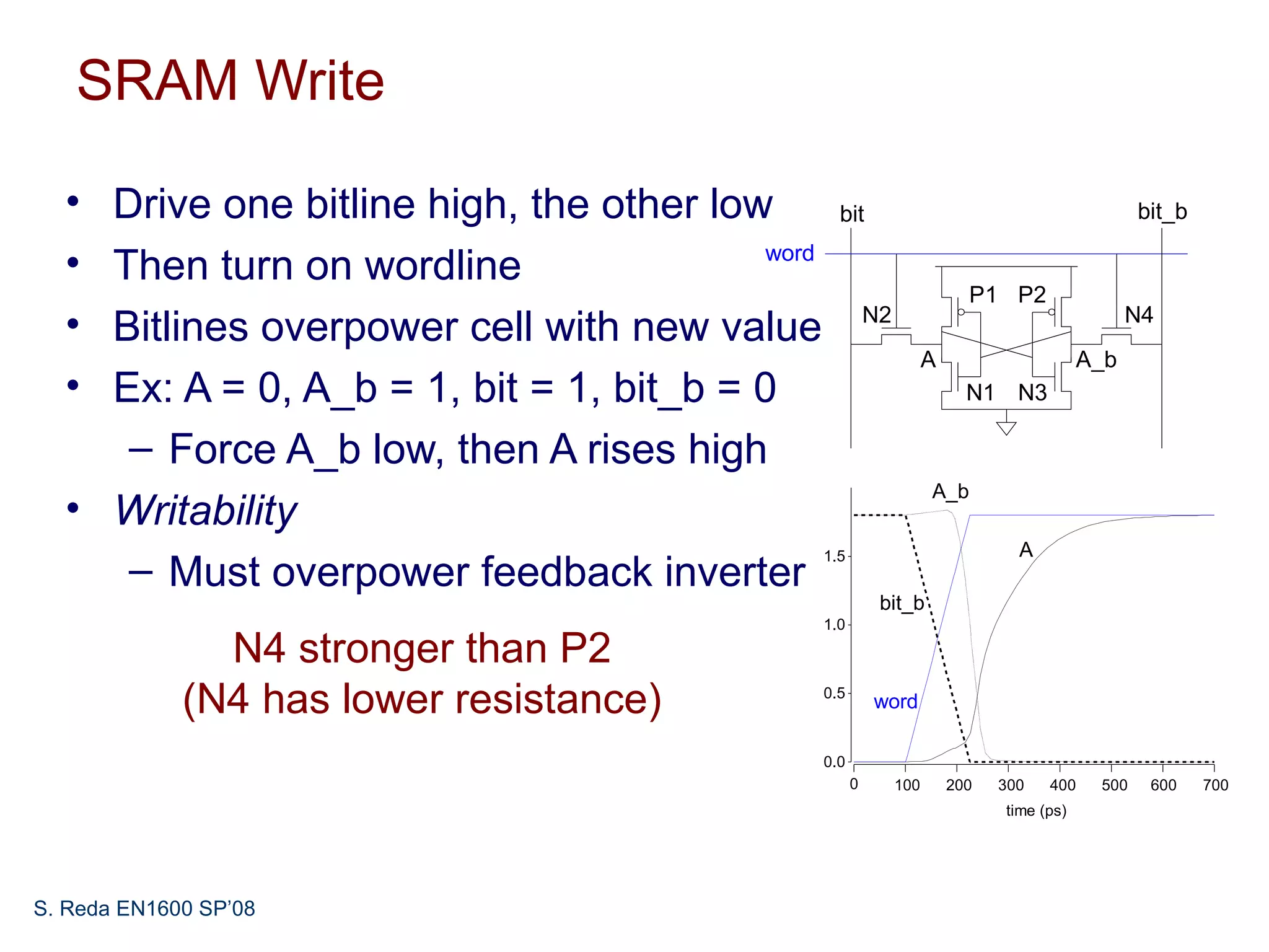
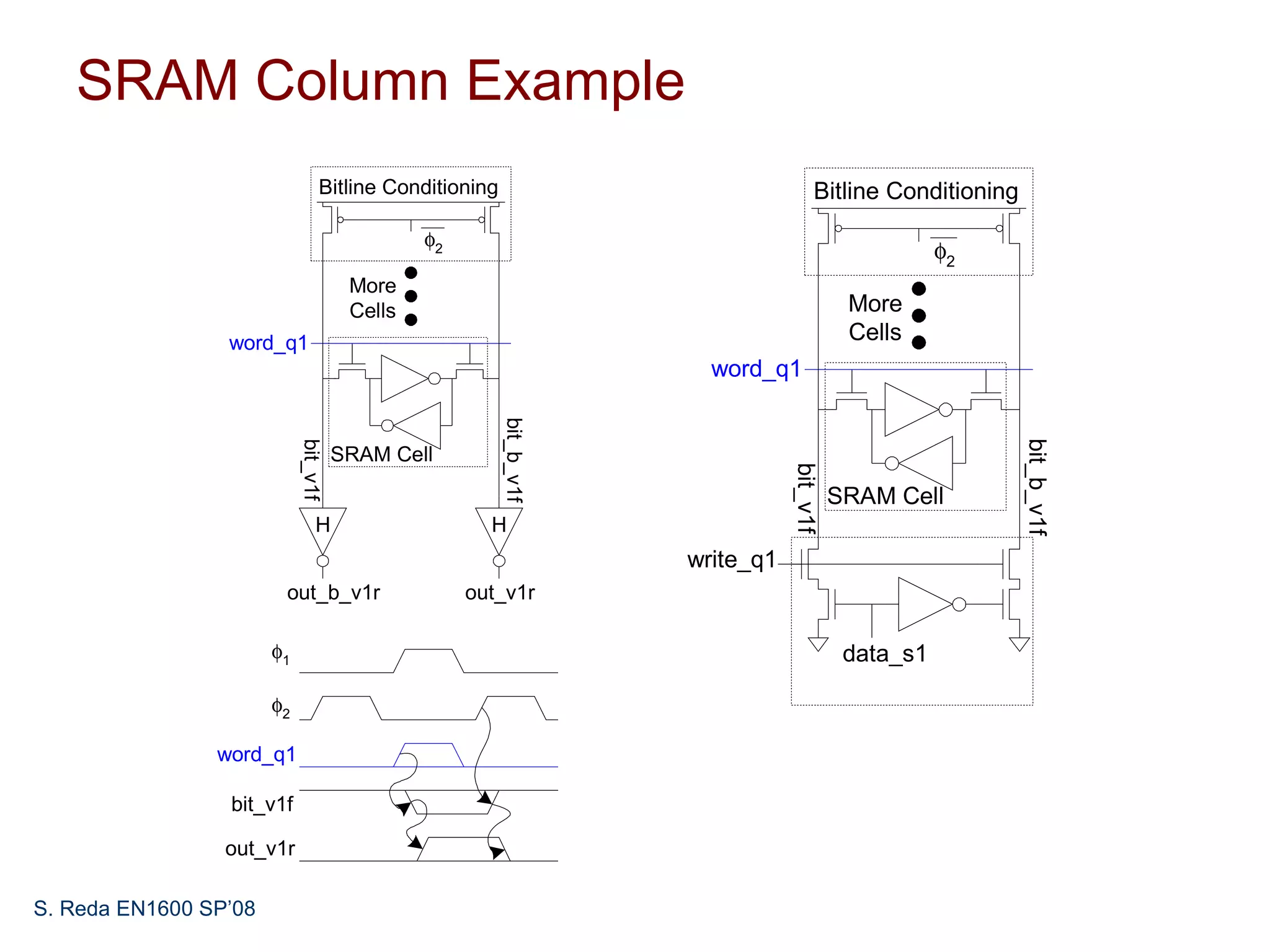
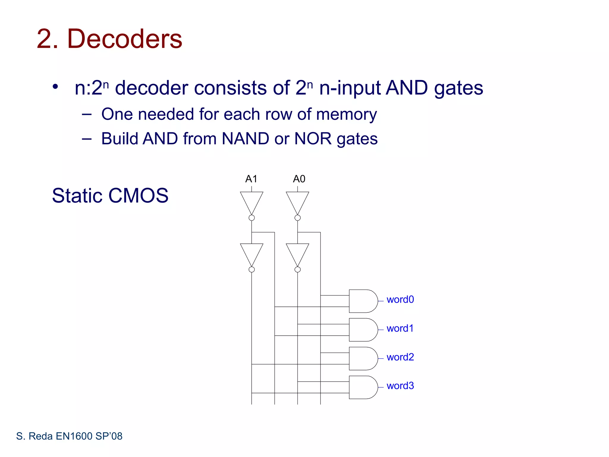
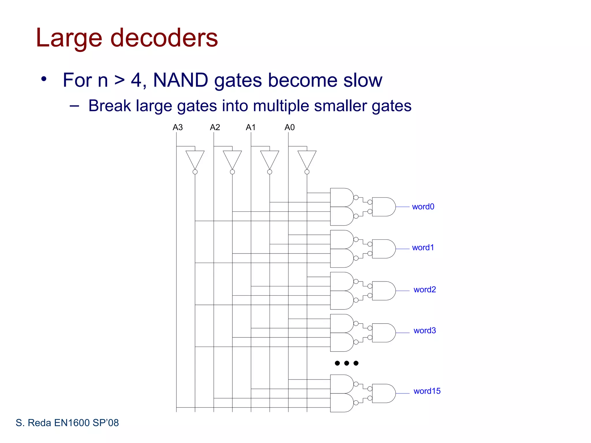
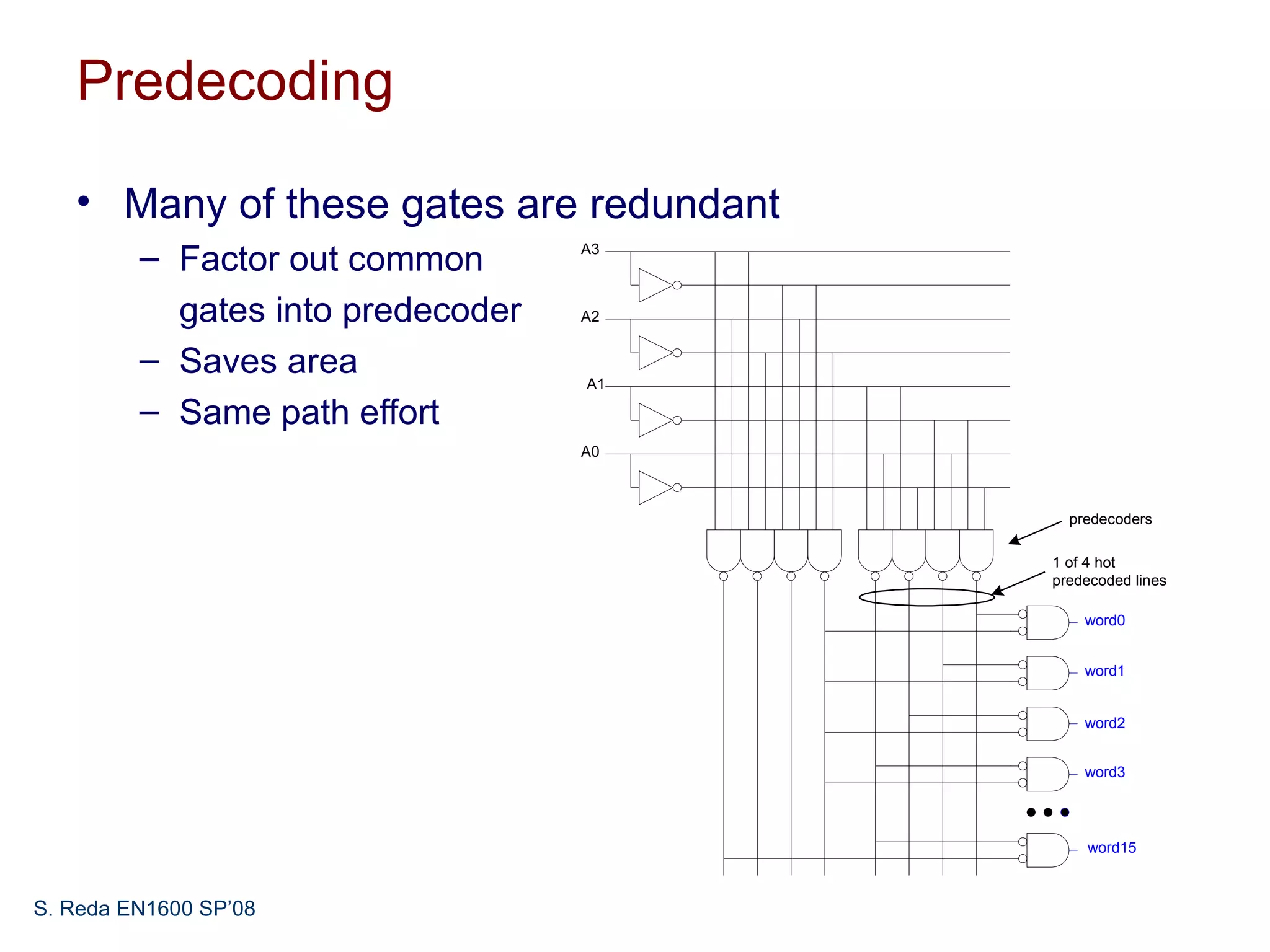
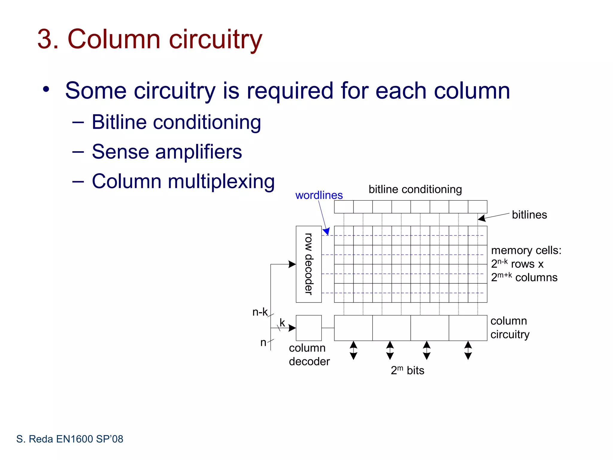
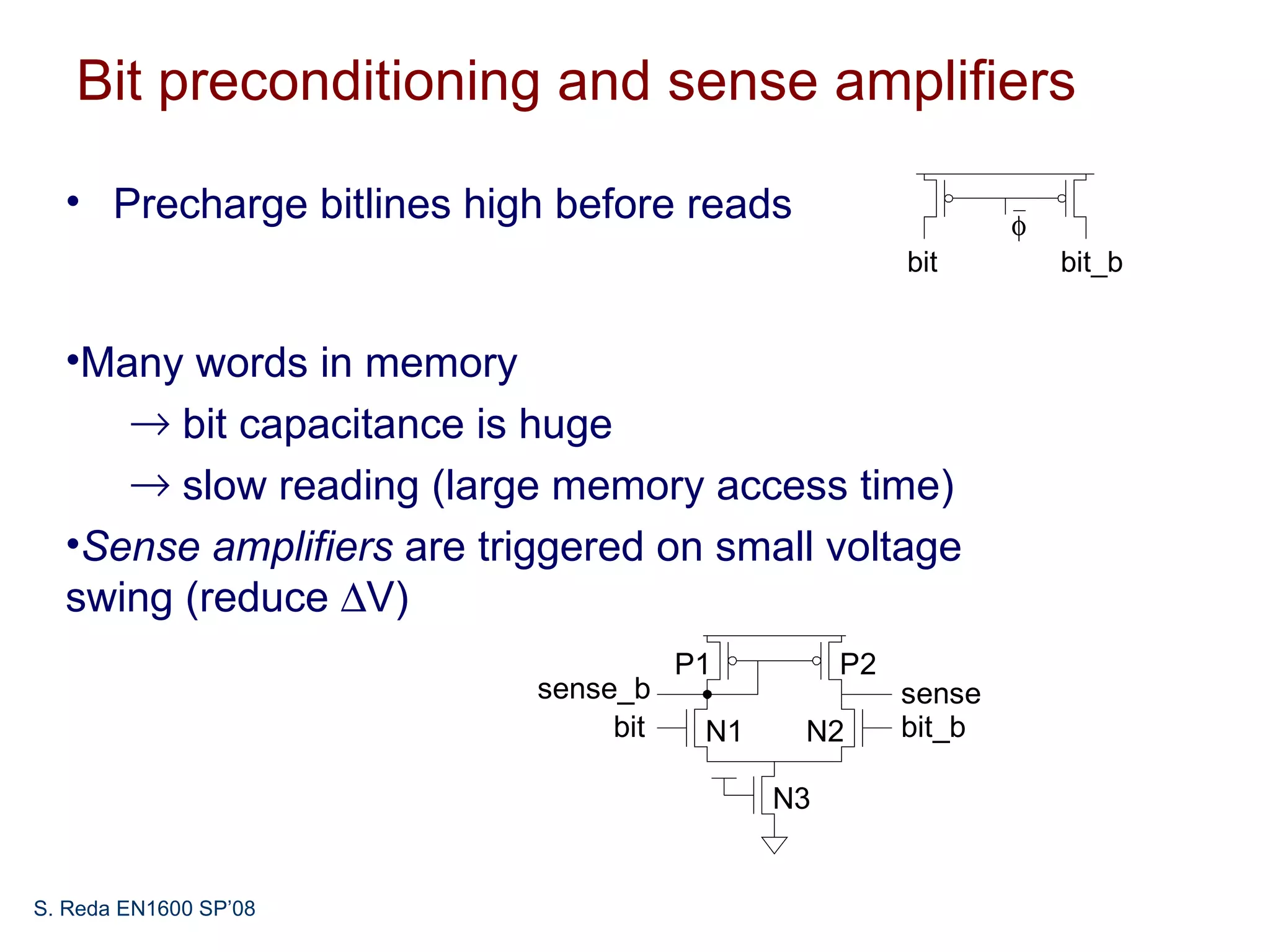
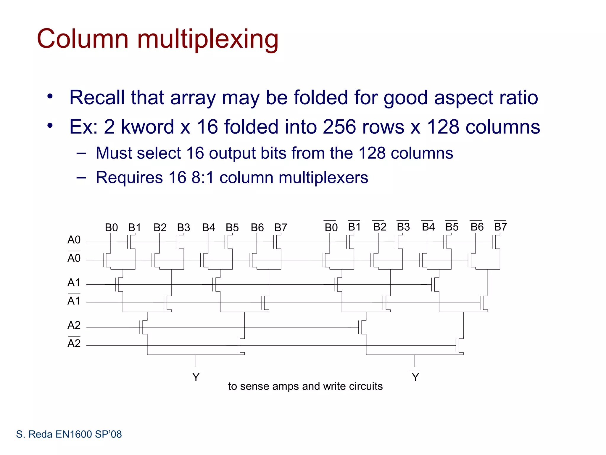
Design and Implementation of VLSI Systems
                   (EN1600)
                Lecture 29: Array Subsystems (SRAM)


S. Reda EN1600 SP’08
Array subsystems


   •    SRAM
   •    DRAM
   •    ROM
   •    FLASH
   •    PLA/FPGA


S. Reda EN1600 SP’08
Array architecture
                               2m bits                                            2m bits

                S0                                                       S0
                              Word 0                                             Word 0
                S1
                              Word 1                  A0                         Word 1
                S2                         Storage                                            Storage
                              Word 2
                                           cell       A1                         Word 2
                                                                                              cell


        word s                                        An-
         N SN -                                             1
                                                                 D ecod er
                       2
                            Word N - 2                                         Word N - 2
               SN -
                            Word N - 1                                         Word N - 1
                       1

                                                     n = log2N


                           Input-O utput                                      Input-O utput
                              (M bits)                                           (M bits)

     Intuitive architecture for N x 2m memory          Decoder reduces the number of select signals
              Too many select signals:
            N words == N select signals
                                                                       n = log 2 N
                                                           Problem: ASPECT RATIO or
                                                           HEIGHT >> WIDTH
S. Reda EN1600 SP’08
Array architecture
      • 2n words of 2m bits each
      • If n >> m, fold by 2k into fewer rows of more columns
                                                 bitline conditioning
                                  wordlines
                                                        3.                  bitlines


                                   row decoder                          memory cells:
                                   2.                1. core            2n-k rows x
                                                                        2m+k columns


                       n-k
                             k                                          column
                                                        3.              circuitry
                        n        column
                                 decoder
                                                     2m bits

      • Good regularity – easy to design
      • Very high density if good cells are used

S. Reda EN1600 SP’08
1. Core. 12T SRAM Cell
    • Basic building block: SRAM Cell
          – Holds one bit of information, like a latch
          – Must be read and written
    • 12-transistor (12T) SRAM cell
          – Use a simple latch connected to bitline
          – 46 x 75 λ unit cell


S. Reda EN1600 SP’08
6T SRAM Cell
   • Cell size accounts for most of array size
         – Reduce cell size at expense of complexity
   • 6T SRAM Cell
         – Used in most commercial chips
         – Data stored in cross-coupled inverters      bit   bit_b
   • Read:                                     word
         – Precharge bit, bit_b
         – Raise wordline
   • Write:
         – Drive data onto bit, bit_b
         – Raise wordline

                                           Size 26 x 45 λ


S. Reda EN1600 SP’08
SRAM Read
    • Precharge both bitlines high
    • Then turn on wordline
    • One of the two bitlines will be
      pulled down by the cell
    • Ex: A = 0, A_b = 1
       – bit discharges, bit_b stays
         high
       – But A bumps up slightly
    • Read stability
       – A must not flip
          N1 stronger than N2
        (N1 has lower resistance)


S. Reda EN1600 SP’08
Reading within the context of a column


S. Reda EN1600 SP’08
SRAM Write

  • Drive one bitline high, the other low         bit                                             bit_b

  • Then turn on wordline                word
                                                                           P1 P2
  • Bitlines overpower cell with new value                N2                                     N4
                                                                     A                     A_b
  • Ex: A = 0, A_b = 1, bit = 1, bit_b = 0                                 N1 N3

     – Force A_b low, then A rises high
                                                                     A_b
  • Writability
                                                                                 A
     – Must overpower feedback inverter
                                                1.5


                                                           bit_b
                                                1.0

               N4 stronger than P2
             (N4 has lower resistance)          0.5
                                                          word

                                                0.0
                                                      0        100       200   300   400    500    600    700
                                                                               time (ps)


S. Reda EN1600 SP’08
SRAM Column Example
                                 Bitline Conditioning                               Bitline Conditioning
                                               φ2
                                                                                                    φ2
                                       More
                                       Cells                                              More
                 word_q1                                                                  Cells
                                                                      word_q1


                                                        bit_b_v1f


                                                                                                           bit_b_v1f
                            bit_v1f


                                      SRAM Cell


                                                                               bit_v1f
                                                                                         SRAM Cell
                                H                     H
                                                                    write_q1
                        out_b_v1r                   out_v1r

                       φ1                                                                 data_s1

                       φ2

                word_q1

                 bit_v1f

                 out_v1r

S. Reda EN1600 SP’08
2. Decoders
      • n:2n decoder consists of 2n n-input AND gates
            – One needed for each row of memory
            – Build AND from NAND or NOR gates

                               A1   A0
      Static CMOS


                                                  word0

                                                  word1

                                                  word2

                                                  word3


S. Reda EN1600 SP’08
Large decoders
    • For n > 4, NAND gates become slow
          – Break large gates into multiple smaller gates
                        A3   A2   A1   A0


                                                            word0


                                                            word1


                                                            word2


                                                            word3


                                                            word15


S. Reda EN1600 SP’08
Predecoding

   • Many of these gates are redundant
         – Factor out common       A3


           gates into predecoder   A2


         – Saves area
                                   A1

         – Same path effort
                                   A0


                                           predecoders

                                         1 of 4 hot
                                         predecoded lines

                                             word0


                                             word1


                                             word2


                                             word3


                                             word15


S. Reda EN1600 SP’08
3. Column circuitry
    • Some circuitry is required for each column
          – Bitline conditioning
          – Sense amplifiers
          – Column multiplexing                        bitline conditioning
                                        wordlines
                                                                                  bitlines


                                         row decoder
                                                                              memory cells:
                                                                              2n-k rows x
                                                                              2m+k columns


                             n-k
                                   k                                          column
                                                                              circuitry
                              n        column
                                       decoder
                                                           2m bits


S. Reda EN1600 SP’08
Bit preconditioning and sense amplifiers

  • Precharge bitlines high before reads                      φ
                                                      bit         bit_b


  •Many words in memory
     → bit capacitance is huge
     → slow reading (large memory access time)
  •Sense amplifiers are triggered on small voltage
  swing (reduce ∆V)
                                      P1         P2
                           sense_b                    sense
                                bit    N1    N2       bit_b

                                            N3


S. Reda EN1600 SP’08
Column multiplexing

     • Recall that array may be folded for good aspect ratio
     • Ex: 2 kword x 16 folded into 256 rows x 128 columns
           – Must select 16 output bits from the 128 columns
           – Requires 16 8:1 column multiplexers

                B0 B1   B2 B3       B4 B5   B6 B7         B0 B1     B2 B3       B4 B5   B6 B7
         A0
         A0

         A1
         A1

         A2
         A2


                                Y                                           Y
                                       to sense amps and write circuits


S. Reda EN1600 SP’08

Lecture29

  • 1.
    Design and Implementationof VLSI Systems (EN1600) Lecture 29: Array Subsystems (SRAM) S. Reda EN1600 SP’08
  • 2.
    Array subsystems • SRAM • DRAM • ROM • FLASH • PLA/FPGA S. Reda EN1600 SP’08
  • 3.
    Array architecture 2m bits 2m bits S0 S0 Word 0 Word 0 S1 Word 1 A0 Word 1 S2 Storage Storage Word 2 cell A1 Word 2 cell word s An- N SN - 1 D ecod er 2 Word N - 2 Word N - 2 SN - Word N - 1 Word N - 1 1 n = log2N Input-O utput Input-O utput (M bits) (M bits) Intuitive architecture for N x 2m memory Decoder reduces the number of select signals Too many select signals: N words == N select signals n = log 2 N Problem: ASPECT RATIO or HEIGHT >> WIDTH S. Reda EN1600 SP’08
  • 4.
    Array architecture • 2n words of 2m bits each • If n >> m, fold by 2k into fewer rows of more columns bitline conditioning wordlines 3. bitlines row decoder memory cells: 2. 1. core 2n-k rows x 2m+k columns n-k k column 3. circuitry n column decoder 2m bits • Good regularity – easy to design • Very high density if good cells are used S. Reda EN1600 SP’08
  • 5.
    1. Core. 12TSRAM Cell • Basic building block: SRAM Cell – Holds one bit of information, like a latch – Must be read and written • 12-transistor (12T) SRAM cell – Use a simple latch connected to bitline – 46 x 75 λ unit cell S. Reda EN1600 SP’08
  • 6.
    6T SRAM Cell • Cell size accounts for most of array size – Reduce cell size at expense of complexity • 6T SRAM Cell – Used in most commercial chips – Data stored in cross-coupled inverters bit bit_b • Read: word – Precharge bit, bit_b – Raise wordline • Write: – Drive data onto bit, bit_b – Raise wordline Size 26 x 45 λ S. Reda EN1600 SP’08
  • 7.
    SRAM Read • Precharge both bitlines high • Then turn on wordline • One of the two bitlines will be pulled down by the cell • Ex: A = 0, A_b = 1 – bit discharges, bit_b stays high – But A bumps up slightly • Read stability – A must not flip N1 stronger than N2 (N1 has lower resistance) S. Reda EN1600 SP’08
  • 8.
    Reading within thecontext of a column S. Reda EN1600 SP’08
  • 9.
    SRAM Write • Drive one bitline high, the other low bit bit_b • Then turn on wordline word P1 P2 • Bitlines overpower cell with new value N2 N4 A A_b • Ex: A = 0, A_b = 1, bit = 1, bit_b = 0 N1 N3 – Force A_b low, then A rises high A_b • Writability A – Must overpower feedback inverter 1.5 bit_b 1.0 N4 stronger than P2 (N4 has lower resistance) 0.5 word 0.0 0 100 200 300 400 500 600 700 time (ps) S. Reda EN1600 SP’08
  • 10.
    SRAM Column Example Bitline Conditioning Bitline Conditioning φ2 φ2 More Cells More word_q1 Cells word_q1 bit_b_v1f bit_b_v1f bit_v1f SRAM Cell bit_v1f SRAM Cell H H write_q1 out_b_v1r out_v1r φ1 data_s1 φ2 word_q1 bit_v1f out_v1r S. Reda EN1600 SP’08
  • 11.
    2. Decoders • n:2n decoder consists of 2n n-input AND gates – One needed for each row of memory – Build AND from NAND or NOR gates A1 A0 Static CMOS word0 word1 word2 word3 S. Reda EN1600 SP’08
  • 12.
    Large decoders • For n > 4, NAND gates become slow – Break large gates into multiple smaller gates A3 A2 A1 A0 word0 word1 word2 word3 word15 S. Reda EN1600 SP’08
  • 13.
    Predecoding • Many of these gates are redundant – Factor out common A3 gates into predecoder A2 – Saves area A1 – Same path effort A0 predecoders 1 of 4 hot predecoded lines word0 word1 word2 word3 word15 S. Reda EN1600 SP’08
  • 14.
    3. Column circuitry • Some circuitry is required for each column – Bitline conditioning – Sense amplifiers – Column multiplexing bitline conditioning wordlines bitlines row decoder memory cells: 2n-k rows x 2m+k columns n-k k column circuitry n column decoder 2m bits S. Reda EN1600 SP’08
  • 15.
    Bit preconditioning andsense amplifiers • Precharge bitlines high before reads φ bit bit_b •Many words in memory → bit capacitance is huge → slow reading (large memory access time) •Sense amplifiers are triggered on small voltage swing (reduce ∆V) P1 P2 sense_b sense bit N1 N2 bit_b N3 S. Reda EN1600 SP’08
  • 16.
    Column multiplexing • Recall that array may be folded for good aspect ratio • Ex: 2 kword x 16 folded into 256 rows x 128 columns – Must select 16 output bits from the 128 columns – Requires 16 8:1 column multiplexers B0 B1 B2 B3 B4 B5 B6 B7 B0 B1 B2 B3 B4 B5 B6 B7 A0 A0 A1 A1 A2 A2 Y Y to sense amps and write circuits S. Reda EN1600 SP’08