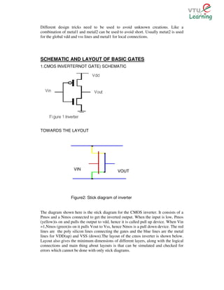
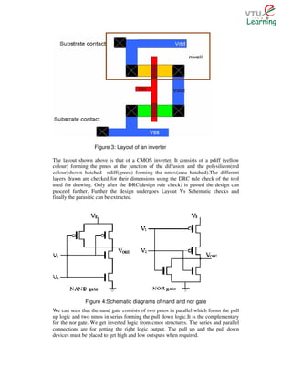
This document provides an overview of the physical design process for integrated circuits. It discusses the steps from schematic design to layout, including floorplanning, placement, routing, and design rule checking. Sample schematics and layouts are shown for basic gates like inverters, NAND gates, and transmission gates. Guidelines are provided for layout optimization to improve performance and density. The layout process involves translating the schematic into distinct layers and ensuring design rules are followed with respect to dimensions, spacing, and connectivity between layers.


![We see that the width is increasing by a factor of f towards the last stage. Now both f
and N can be complementary. If f for each stage is large the number of stages N
reduces but delay per stage increases. Therefore it becomes essential to optimize. Fix
N and find the minimum value of f. For nmos inverters if the input transitions from 0
to 1 the delay is fƐ and if it transitions from 1 to 0 the delay is 4 fƐ. The delay for a
nmos pair is 5 fƐ. For a cmos pair it will be 7fƐ
optimum value of f.
Assume y=CL/ Cg = fN, therefore choice of values of N and f are interdependent.
ロ
We find the value of f to minimize the delay, from the equation of y we have
ln(y)=Nln(f) i.e N=ln(y)/ln(f). If delay per stage is 5fƐ for nmos, then for even
number of stages the total delay is N/2 5fƐ=2.5fƐ. For cmos total delay is N/2 7fƐ =
3.5fƐ
Hence delay ά Nft=ln(y)/ln(f)ft. Delay can be minimized if chose the value of f to be
equal to e which is the base of natural logarithms. It means that each stage is 2.7wider
than its predecessor. If f=e then N= ln(y).The total delay is then given by
1.For N=even
td=2.5NeƐ for nmos, td=3.5NeƐ for cmos
2.For N=odd
transition from 0 to 1 transition from1 to 0
td=[2.5(N-1)+1]eƐ nmos td=[2.5(N-1)+4]eƐ
td=[3.59N-1)+2]eƐ cmos td=[3.5(N-1)+5]eƐ
for example
For N=5 which is odd we can calculate the delay fro vin=1 as td=[2.5(5-1)+1]eƐ
=11e Ɛ
i.e. 1 +4+1+4+1 = 11eƐ
For vin =0 , td=[2.5(5-1)+4]eƐ = 14eƐ
4+1+4+1+4 = 14eƐ
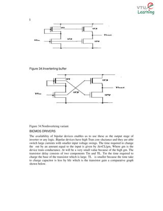
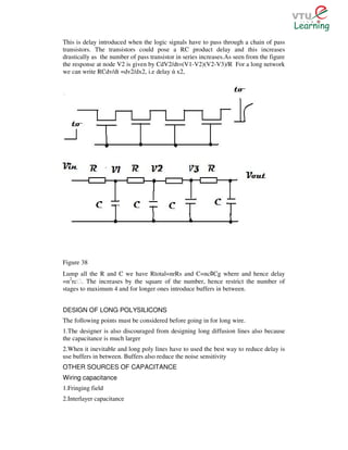
SUPER BUFFER
The asymmetry of the inverters used to solve delay problems is clearly undesirable,
this also leads to more delay problems, super buffer are a better solution. We have a
inverting and non inverting variants of the super buffer. Such arrangements when
used for 5u technology showed that they were capable of driving 2pf capacitance with
2nsec rise time.The figure shown next is the inverting variant.](https://image.slidesharecdn.com/cmosuma-111222025611-phpapp01/85/Cmos-uma-27-320.jpg)


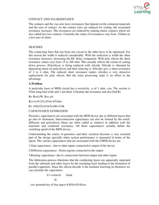
![RF Circuit Design - [Ch2-1] Resonator and Impedance Matching](https://cdn.slidesharecdn.com/ss_thumbnails/ch2-1-150613064353-lva1-app6892-thumbnail.jpg?width=640&height=640&fit=bounds)