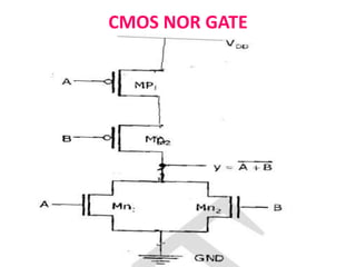
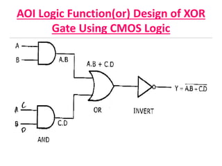
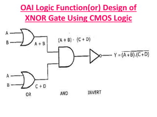
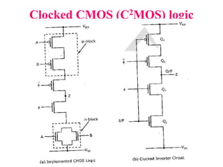
SlideShare a Scribd company logo
VLSI-GATE LEVEL DESIGN
-BY N.C.CHANDU PRASANTH
General Logic Circuit
General Logic Circuit:
CMOS STATIC LOGIC
CMOS INVERTER
WORKING OF CMOS INVERTER
Explanation of Working Operation
CMOS NOR GATE
Working of CMOS NOR Gate
CMOS NAND GATE
Working of CMOS NAND Gate
Complex Gates in CMOS Logic
AOI Logic Function(or) Design of XOR
Gate Using CMOS Logic
CMOS Implementation
Steps for CMOS Implementation
OAI Logic Function(or) Design of
XNOR Gate Using CMOS Logic
CMOS Implementation
Switch Logic
Pass Transistor
Advantages &Disadvantages of Pass
Transistor
Pass Transistor Logic(PTL)
• Only N_MOS Transistors are Used to design the logic.
• Input Signals are Applied to both Gate and
Drain/Source.
When A=1 Upper NMOS is ON, So
o/p is F=B
When A=0 Upper
NMOS is ON, So o/p is F=B
CMOS Transmission Gate
 Actually, It is a Parallel Connection of
N_MOSFET and P-MOSFET that realizes a
simple switch.
 Inputs to the gates of N-MOSFET and P-
MOSFET are Complementary to each other.
Working of CMOS Transmission Gate
Case-1
When C=1 and C^=0
Both NMOS&PMOS--------ON
 Nodes A&B-----------Short Circuited
Input Logic is Transferred to Output
Case-2
When C=10and C^=1
Both NMOS&PMOS--------OFF
 Nodes A&B-----------Open Circuited
Actually ,this is Called High-Impedance State.
Transmission Gate Symbol
Operation of Transmission Gate
Advantages &Disadvantages of
Transmission Gate
2- input Multiplexer using CMOS
Transmission Gates
Working
Alternative Gate Circuits
ALTERNATIVE GATE CIRCUITS
1. Pseudo- NMOS logic
2. Dynamic CMOS logic
(Pseudo –NMOS+NMOS Transistor)
3. Clocked CMOS (C2MOS) logic
4. CMOS domino logic
(Dynamic CMOS + Inveter)
5. n-p CMOS logic
General form of Pseudo- NMOS logic
G
Description
 It is used as a supplement for the CMOS logic circuits.
 In the pseudo-NMOS logic, the PUN is realized by a
single PMOS transistor.
The gate terminal of the PMOS transistor is connected
to the ground.
P-MOS Transistor remains permanently in the ON state
Depending on the input combinations, output goes low
through the PDN.
Only the NMOS logic (Qn) is driven by the input
Voltage
Qp acts as an active load for Qn.
Except for the load device(P-MOS), the Pseudo-NMOS
gate circuit is identical to the pull-down
network(PDN) of the CMOS gate.
Realization of logic circuits using Pseudo-NMOS logic
Advantages & Disadvantages of Pseudo N-MOS Logic
Advantages:
1) Uses less number of transistors as compared to
CMOS logic.
2) Geometrical area and delay gets reduced as it
requires less transistors.
3) Low power dissipation.
Disadvantages
1.The main drawback of using a Pseudo NMOS gate
instead of a CMOS gate is that the always on PMOS
load conducts a steady current when the output
voltage is lower than VDD.
2.Layout problems are critical.
General form of Dynamic CMOS logic
Description
 It is one of the alternate method of reducing
Transistor Count.
It is similar to Pseudo –NMOS Logic except one
additional NMOS Transistor(MN) Connected between
PDN and Ground.
PMOS Transistor in PUN and additional NMOS
Transistor(MN) in PDN are Operated by a Clock Signal
ϕ.
Dynamic Logic Circuit Operates in 2 Phases of Single
Clock Pulse ϕ
Phase-1 (Pre-Charge Phase ϕ =0)
Here, Output is Pre Charged to Logic High Level.
Phase-2 (Evaluation Phase ϕ=1)
Here, Output is evaluated based on applied Input Logic.
Dynamic CMOS Logic Example
Disadvantages of Dynamic CMOS logic
Dynamic CMOS Circuit has a Serious Problem
When they are cascaded.
Advantages of Dynamic CMOS logic
General form of CMOS Domino Logic
(Dynamic Logic + Inverter)
ϕ
Description
 It is a Slightly modified Version of Dynamic CMOS
Logic Circuit.
A Static Inverter is Connected at the Output of
each dynamic CMOS logic blocks.
Addition of Inverter Solves the Problem of
Cascading of dynamic CMOS logic Circuits.
 It is Suitable for only Non-Inverting Logic(the
expression having no complement over whole
expression)
For Inverting the logic the expression must be
reorganized before it can be realized using
Domino CMOS Logic.
Working
Case -1 when ϕ = 0
Output is Pre charged to logic high and O/P of static
Inverter is Low.
Case -2 When ϕ =1
O/P is either 0 (or) 1 Output of static Inverter
can make 0 1 in Evaluation. So, Irrespective of I/P
and O/p of Static Inverter can’t make 1 0 in
Evaluation Phase.
Note:
For, N- Input Logic function we require,
2N Transistors-- Static CMOS
N+2 Transistors- Dynamic CMOS
N+2+2 Transistors Domino CMOS
Example of Domino CMOS Logic
Clocked CMOS (C2MOS) logic
Description
A pull-up p-block and a complementary n-block pull-
down structure represent p and n-transistors
However, the logic in this case is connected to the
output only during the ON period of the clock.
Working
When ø = 1 the circuit acts an inverter , because
transistors Q3 and Q4 are ‘ON’ .
 It is said to be in the “Evaluation mode”. Therefore
the output Z changes its Previous value.
When ø = 0 the circuit is in hold mode, because
transistors Q3 and Q4 ‘OFF’ .
It is said to be in the “Pre Charge mode”. Therefore
the output Z remains its previous value.
n-p CMOS logic (NORA)
Description
In this, logic the actual logic blocks are
alternatively ‘n’ and ‘p’ in a cascaded structure.
The clock ø and ø^ are used alternatively to fed
the Pre Charge and Evaluate transistors.
Disadvantages of N-P CMOS Logic
Here, the P-tree blocks are slower than the
N-tree modules, due to the lower current drive
of the PMOS transistors in the logic network.

More Related Content

What's hot

Vlsi Summer training report pdf
Vlsi Summer training report pdfVlsi Summer training report pdf
Vlsi Summer training report pdf
GirjeshVerma2
 
Lambda design rule
Lambda design ruleLambda design rule
Lambda design rule
Gowri Kishore
 
Driving large capacitive loads
Driving large capacitive loadsDriving large capacitive loads
Driving large capacitive loads
Ravi Selvaraj
 
VLSI Testing Techniques
VLSI Testing TechniquesVLSI Testing Techniques
VLSI Testing Techniques
A B Shinde
 
Layout & Stick Diagram Design Rules
Layout & Stick Diagram Design RulesLayout & Stick Diagram Design Rules
Layout & Stick Diagram Design Rules
varun kumar
 
Mos transistor
Mos transistorMos transistor
Mos transistor
Murali Rai
 
Waveform coding
Waveform codingWaveform coding
Waveform coding
Alapan Banerjee
 
VLSI circuit design process
VLSI circuit design processVLSI circuit design process
VLSI circuit design process
Vishal kakade
 
Stick Diagram and Lambda Based Design Rules
Stick Diagram and Lambda Based Design RulesStick Diagram and Lambda Based Design Rules
Stick Diagram and Lambda Based Design Rules
Tahsin Al Mahi
 
VLSI Design Sequential circuit design
VLSI Design Sequential circuit designVLSI Design Sequential circuit design
VLSI Design Sequential circuit design
tamil arasan
 
Low power vlsi design ppt
Low power vlsi design pptLow power vlsi design ppt
Low power vlsi design ppt
Anil Yadav
 
Combinational Logic
Combinational LogicCombinational Logic
Combinational Logic
Sirat Mahmood
 
CELLULAR MOBILE RADIO SYSTEMS
CELLULAR MOBILE RADIO SYSTEMSCELLULAR MOBILE RADIO SYSTEMS
CELLULAR MOBILE RADIO SYSTEMS
VenkataSatya Manchikalapati
 
VLSI Technology Evolution
VLSI Technology EvolutionVLSI Technology Evolution
VLSI Technology Evolution
A B Shinde
 
BUilt-In-Self-Test for VLSI Design
BUilt-In-Self-Test for VLSI DesignBUilt-In-Self-Test for VLSI Design
BUilt-In-Self-Test for VLSI Design
Usha Mehta
 
Short Channel Effect In MOSFET
Short Channel Effect In MOSFETShort Channel Effect In MOSFET
Short Channel Effect In MOSFET
Sudhanshu Srivastava
 
Hardware description languages
Hardware description languagesHardware description languages
Hardware description languages
Akhila Rahul
 
The cellular concept
The cellular conceptThe cellular concept
The cellular concept
ZunAib Ali
 
Lecture11 combinational logic dynamics
Lecture11 combinational logic dynamicsLecture11 combinational logic dynamics
Lecture11 combinational logic dynamics
vidhya DS
 
Embedded firmware
Embedded firmwareEmbedded firmware
Embedded firmware
Joel P
 

What's hot (20)

Vlsi Summer training report pdf
Vlsi Summer training report pdfVlsi Summer training report pdf
Vlsi Summer training report pdf
 
Lambda design rule
Lambda design ruleLambda design rule
Lambda design rule
 
Driving large capacitive loads
Driving large capacitive loadsDriving large capacitive loads
Driving large capacitive loads
 
VLSI Testing Techniques
VLSI Testing TechniquesVLSI Testing Techniques
VLSI Testing Techniques
 
Layout & Stick Diagram Design Rules
Layout & Stick Diagram Design RulesLayout & Stick Diagram Design Rules
Layout & Stick Diagram Design Rules
 
Mos transistor
Mos transistorMos transistor
Mos transistor
 
Waveform coding
Waveform codingWaveform coding
Waveform coding
 
VLSI circuit design process
VLSI circuit design processVLSI circuit design process
VLSI circuit design process
 
Stick Diagram and Lambda Based Design Rules
Stick Diagram and Lambda Based Design RulesStick Diagram and Lambda Based Design Rules
Stick Diagram and Lambda Based Design Rules
 
VLSI Design Sequential circuit design
VLSI Design Sequential circuit designVLSI Design Sequential circuit design
VLSI Design Sequential circuit design
 
Low power vlsi design ppt
Low power vlsi design pptLow power vlsi design ppt
Low power vlsi design ppt
 
Combinational Logic
Combinational LogicCombinational Logic
Combinational Logic
 
CELLULAR MOBILE RADIO SYSTEMS
CELLULAR MOBILE RADIO SYSTEMSCELLULAR MOBILE RADIO SYSTEMS
CELLULAR MOBILE RADIO SYSTEMS
 
VLSI Technology Evolution
VLSI Technology EvolutionVLSI Technology Evolution
VLSI Technology Evolution
 
BUilt-In-Self-Test for VLSI Design
BUilt-In-Self-Test for VLSI DesignBUilt-In-Self-Test for VLSI Design
BUilt-In-Self-Test for VLSI Design
 
Short Channel Effect In MOSFET
Short Channel Effect In MOSFETShort Channel Effect In MOSFET
Short Channel Effect In MOSFET
 
Hardware description languages
Hardware description languagesHardware description languages
Hardware description languages
 
The cellular concept
The cellular conceptThe cellular concept
The cellular concept
 
Lecture11 combinational logic dynamics
Lecture11 combinational logic dynamicsLecture11 combinational logic dynamics
Lecture11 combinational logic dynamics
 
Embedded firmware
Embedded firmwareEmbedded firmware
Embedded firmware
 

Similar to Vlsi gate level design

CMOS logic circuits
CMOS logic circuitsCMOS logic circuits
CMOS logic circuits
Mahesh_Naidu
 
ppt.ppt on didgital logic design by muskan.s
ppt.ppt on didgital logic design by muskan.sppt.ppt on didgital logic design by muskan.s
ppt.ppt on didgital logic design by muskan.s
muskans14
 
A Survey Analysis on CMOS Integrated Circuits with Clock-Gated Logic Structure
A Survey Analysis on CMOS Integrated Circuits with Clock-Gated Logic StructureA Survey Analysis on CMOS Integrated Circuits with Clock-Gated Logic Structure
A Survey Analysis on CMOS Integrated Circuits with Clock-Gated Logic Structure
IJERA Editor
 
Dynamic CMOS.pdf
Dynamic CMOS.pdfDynamic CMOS.pdf
Dynamic CMOS.pdf
RukminiKatreepalli1
 
MetroScientific Week 1.pptx
MetroScientific Week 1.pptxMetroScientific Week 1.pptx
MetroScientific Week 1.pptx
Bipin Saha
 
2. Unit1-CMOS PTL TGL Logic.pdf
2. Unit1-CMOS PTL TGL Logic.pdf2. Unit1-CMOS PTL TGL Logic.pdf
2. Unit1-CMOS PTL TGL Logic.pdf
theanmolchawla19
 
presentation on high-performance_dynamic_cmos_circuit
presentation on high-performance_dynamic_cmos_circuitpresentation on high-performance_dynamic_cmos_circuit
presentation on high-performance_dynamic_cmos_circuit
JayminSojitra
 
Vlsi
VlsiVlsi
ECE 467 Mini project 1
ECE 467 Mini project 1ECE 467 Mini project 1
ECE 467 Mini project 1
Lakshmi Yasaswi Kamireddy
 
Unit no. 5 cmos logic design
Unit no. 5 cmos logic designUnit no. 5 cmos logic design
Unit no. 5 cmos logic design
swagatkarve
 
Dynamic logic circuits
Dynamic logic circuitsDynamic logic circuits
Dynamic logic circuits
Kalyan Kumar Kalita
 
circuit families in vlsi.pptx
circuit families in vlsi.pptxcircuit families in vlsi.pptx
circuit families in vlsi.pptx
anitha862251
 
CMOS Combinational_Logic_Circuits.pdf
CMOS Combinational_Logic_Circuits.pdfCMOS Combinational_Logic_Circuits.pdf
CMOS Combinational_Logic_Circuits.pdf
SouravRoyElectronics
 
STUCK-OPEN FAULT ANALYSIS IN CMOS TRANSISTOR BASED COMBINATIONAL CIRCUITS
STUCK-OPEN FAULT ANALYSIS IN CMOS TRANSISTOR BASED COMBINATIONAL CIRCUITSSTUCK-OPEN FAULT ANALYSIS IN CMOS TRANSISTOR BASED COMBINATIONAL CIRCUITS
STUCK-OPEN FAULT ANALYSIS IN CMOS TRANSISTOR BASED COMBINATIONAL CIRCUITS
Minh Anh Nguyen
 
STUCK-OPEN FAULT ANALYSIS IN CMOS TRANSISTOR BASED COMBINATIONAL CIRCUITS
STUCK-OPEN FAULT ANALYSIS IN CMOS TRANSISTOR BASED COMBINATIONAL CIRCUITSSTUCK-OPEN FAULT ANALYSIS IN CMOS TRANSISTOR BASED COMBINATIONAL CIRCUITS
STUCK-OPEN FAULT ANALYSIS IN CMOS TRANSISTOR BASED COMBINATIONAL CIRCUITS
Minh Anh Nguyen
 
CMOS Topic 6 -_designing_combinational_logic_circuits
CMOS Topic 6 -_designing_combinational_logic_circuitsCMOS Topic 6 -_designing_combinational_logic_circuits
CMOS Topic 6 -_designing_combinational_logic_circuits
Ikhwan_Fakrudin
 
Pipelining approach
Pipelining approachPipelining approach
Pipelining approach
GopinathD17
 
UNIT-4-Logic styles for low power_part_2.ppt
UNIT-4-Logic styles for low power_part_2.pptUNIT-4-Logic styles for low power_part_2.ppt
UNIT-4-Logic styles for low power_part_2.ppt
Ravi Selvaraj
 
CMOS
CMOS CMOS
Lec4 Intro to Computer Engineering by Hsien-Hsin Sean Lee Georgia Tech -- CMOS
Lec4 Intro to Computer Engineering by Hsien-Hsin Sean Lee Georgia Tech -- CMOSLec4 Intro to Computer Engineering by Hsien-Hsin Sean Lee Georgia Tech -- CMOS
Lec4 Intro to Computer Engineering by Hsien-Hsin Sean Lee Georgia Tech -- CMOS
Hsien-Hsin Sean Lee, Ph.D.
 

Similar to Vlsi gate level design (20)

CMOS logic circuits
CMOS logic circuitsCMOS logic circuits
CMOS logic circuits
 
ppt.ppt on didgital logic design by muskan.s
ppt.ppt on didgital logic design by muskan.sppt.ppt on didgital logic design by muskan.s
ppt.ppt on didgital logic design by muskan.s
 
A Survey Analysis on CMOS Integrated Circuits with Clock-Gated Logic Structure
A Survey Analysis on CMOS Integrated Circuits with Clock-Gated Logic StructureA Survey Analysis on CMOS Integrated Circuits with Clock-Gated Logic Structure
A Survey Analysis on CMOS Integrated Circuits with Clock-Gated Logic Structure
 
Dynamic CMOS.pdf
Dynamic CMOS.pdfDynamic CMOS.pdf
Dynamic CMOS.pdf
 
MetroScientific Week 1.pptx
MetroScientific Week 1.pptxMetroScientific Week 1.pptx
MetroScientific Week 1.pptx
 
2. Unit1-CMOS PTL TGL Logic.pdf
2. Unit1-CMOS PTL TGL Logic.pdf2. Unit1-CMOS PTL TGL Logic.pdf
2. Unit1-CMOS PTL TGL Logic.pdf
 
presentation on high-performance_dynamic_cmos_circuit
presentation on high-performance_dynamic_cmos_circuitpresentation on high-performance_dynamic_cmos_circuit
presentation on high-performance_dynamic_cmos_circuit
 
Vlsi
VlsiVlsi
Vlsi
 
ECE 467 Mini project 1
ECE 467 Mini project 1ECE 467 Mini project 1
ECE 467 Mini project 1
 
Unit no. 5 cmos logic design
Unit no. 5 cmos logic designUnit no. 5 cmos logic design
Unit no. 5 cmos logic design
 
Dynamic logic circuits
Dynamic logic circuitsDynamic logic circuits
Dynamic logic circuits
 
circuit families in vlsi.pptx
circuit families in vlsi.pptxcircuit families in vlsi.pptx
circuit families in vlsi.pptx
 
CMOS Combinational_Logic_Circuits.pdf
CMOS Combinational_Logic_Circuits.pdfCMOS Combinational_Logic_Circuits.pdf
CMOS Combinational_Logic_Circuits.pdf
 
STUCK-OPEN FAULT ANALYSIS IN CMOS TRANSISTOR BASED COMBINATIONAL CIRCUITS
STUCK-OPEN FAULT ANALYSIS IN CMOS TRANSISTOR BASED COMBINATIONAL CIRCUITSSTUCK-OPEN FAULT ANALYSIS IN CMOS TRANSISTOR BASED COMBINATIONAL CIRCUITS
STUCK-OPEN FAULT ANALYSIS IN CMOS TRANSISTOR BASED COMBINATIONAL CIRCUITS
 
STUCK-OPEN FAULT ANALYSIS IN CMOS TRANSISTOR BASED COMBINATIONAL CIRCUITS
STUCK-OPEN FAULT ANALYSIS IN CMOS TRANSISTOR BASED COMBINATIONAL CIRCUITSSTUCK-OPEN FAULT ANALYSIS IN CMOS TRANSISTOR BASED COMBINATIONAL CIRCUITS
STUCK-OPEN FAULT ANALYSIS IN CMOS TRANSISTOR BASED COMBINATIONAL CIRCUITS
 
CMOS Topic 6 -_designing_combinational_logic_circuits
CMOS Topic 6 -_designing_combinational_logic_circuitsCMOS Topic 6 -_designing_combinational_logic_circuits
CMOS Topic 6 -_designing_combinational_logic_circuits
 
Pipelining approach
Pipelining approachPipelining approach
Pipelining approach
 
UNIT-4-Logic styles for low power_part_2.ppt
UNIT-4-Logic styles for low power_part_2.pptUNIT-4-Logic styles for low power_part_2.ppt
UNIT-4-Logic styles for low power_part_2.ppt
 
CMOS
CMOS CMOS
CMOS
 
Lec4 Intro to Computer Engineering by Hsien-Hsin Sean Lee Georgia Tech -- CMOS
Lec4 Intro to Computer Engineering by Hsien-Hsin Sean Lee Georgia Tech -- CMOSLec4 Intro to Computer Engineering by Hsien-Hsin Sean Lee Georgia Tech -- CMOS
Lec4 Intro to Computer Engineering by Hsien-Hsin Sean Lee Georgia Tech -- CMOS
 

Recently uploaded

Nuclear Power Economics and Structuring 2024
Nuclear Power Economics and Structuring 2024Nuclear Power Economics and Structuring 2024
Nuclear Power Economics and Structuring 2024
Massimo Talia
 
Standard Reomte Control Interface - Neometrix
Standard Reomte Control Interface - NeometrixStandard Reomte Control Interface - Neometrix
Standard Reomte Control Interface - Neometrix
Neometrix_Engineering_Pvt_Ltd
 
addressing modes in computer architecture
addressing modes  in computer architectureaddressing modes  in computer architecture
addressing modes in computer architecture
ShahidSultan24
 
Student information management system project report ii.pdf
Student information management system project report ii.pdfStudent information management system project report ii.pdf
Student information management system project report ii.pdf
Kamal Acharya
 
Quality defects in TMT Bars, Possible causes and Potential Solutions.
Quality defects in TMT Bars, Possible causes and Potential Solutions.Quality defects in TMT Bars, Possible causes and Potential Solutions.
Quality defects in TMT Bars, Possible causes and Potential Solutions.
PrashantGoswami42
 
CME397 Surface Engineering- Professional Elective
CME397 Surface Engineering- Professional ElectiveCME397 Surface Engineering- Professional Elective
CME397 Surface Engineering- Professional Elective
karthi keyan
 
Sachpazis:Terzaghi Bearing Capacity Estimation in simple terms with Calculati...
Sachpazis:Terzaghi Bearing Capacity Estimation in simple terms with Calculati...Sachpazis:Terzaghi Bearing Capacity Estimation in simple terms with Calculati...
Sachpazis:Terzaghi Bearing Capacity Estimation in simple terms with Calculati...
Dr.Costas Sachpazis
 
在线办理(ANU毕业证书)澳洲国立大学毕业证录取通知书一模一样
在线办理(ANU毕业证书)澳洲国立大学毕业证录取通知书一模一样在线办理(ANU毕业证书)澳洲国立大学毕业证录取通知书一模一样
在线办理(ANU毕业证书)澳洲国立大学毕业证录取通知书一模一样
obonagu
 
road safety engineering r s e unit 3.pdf
road safety engineering  r s e unit 3.pdfroad safety engineering  r s e unit 3.pdf
road safety engineering r s e unit 3.pdf
VENKATESHvenky89705
 
Forklift Classes Overview by Intella Parts
Forklift Classes Overview by Intella PartsForklift Classes Overview by Intella Parts
Forklift Classes Overview by Intella Parts
Intella Parts
 
一比一原版(SFU毕业证)西蒙菲莎大学毕业证成绩单如何办理
一比一原版(SFU毕业证)西蒙菲莎大学毕业证成绩单如何办理一比一原版(SFU毕业证)西蒙菲莎大学毕业证成绩单如何办理
一比一原版(SFU毕业证)西蒙菲莎大学毕业证成绩单如何办理
bakpo1
 
Halogenation process of chemical process industries
Halogenation process of chemical process industriesHalogenation process of chemical process industries
Halogenation process of chemical process industries
MuhammadTufail242431
 
Democratizing Fuzzing at Scale by Abhishek Arya
Democratizing Fuzzing at Scale by Abhishek AryaDemocratizing Fuzzing at Scale by Abhishek Arya
Democratizing Fuzzing at Scale by Abhishek Arya
abh.arya
 
The Benefits and Techniques of Trenchless Pipe Repair.pdf
The Benefits and Techniques of Trenchless Pipe Repair.pdfThe Benefits and Techniques of Trenchless Pipe Repair.pdf
The Benefits and Techniques of Trenchless Pipe Repair.pdf
Pipe Restoration Solutions
 
Top 10 Oil and Gas Projects in Saudi Arabia 2024.pdf
Top 10 Oil and Gas Projects in Saudi Arabia 2024.pdfTop 10 Oil and Gas Projects in Saudi Arabia 2024.pdf
Top 10 Oil and Gas Projects in Saudi Arabia 2024.pdf
Teleport Manpower Consultant
 
ethical hacking in wireless-hacking1.ppt
ethical hacking in wireless-hacking1.pptethical hacking in wireless-hacking1.ppt
ethical hacking in wireless-hacking1.ppt
Jayaprasanna4
 
power quality voltage fluctuation UNIT - I.pptx
power quality voltage fluctuation UNIT - I.pptxpower quality voltage fluctuation UNIT - I.pptx
power quality voltage fluctuation UNIT - I.pptx
ViniHema
 
Water Industry Process Automation and Control Monthly - May 2024.pdf
Water Industry Process Automation and Control Monthly - May 2024.pdfWater Industry Process Automation and Control Monthly - May 2024.pdf
Water Industry Process Automation and Control Monthly - May 2024.pdf
Water Industry Process Automation & Control
 
Final project report on grocery store management system..pdf
Final project report on grocery store management system..pdfFinal project report on grocery store management system..pdf
Final project report on grocery store management system..pdf
Kamal Acharya
 
ASME IX(9) 2007 Full Version .pdf
ASME IX(9)  2007 Full Version       .pdfASME IX(9)  2007 Full Version       .pdf
ASME IX(9) 2007 Full Version .pdf
AhmedHussein950959
 

Recently uploaded (20)

Nuclear Power Economics and Structuring 2024
Nuclear Power Economics and Structuring 2024Nuclear Power Economics and Structuring 2024
Nuclear Power Economics and Structuring 2024
 
Standard Reomte Control Interface - Neometrix
Standard Reomte Control Interface - NeometrixStandard Reomte Control Interface - Neometrix
Standard Reomte Control Interface - Neometrix
 
addressing modes in computer architecture
addressing modes  in computer architectureaddressing modes  in computer architecture
addressing modes in computer architecture
 
Student information management system project report ii.pdf
Student information management system project report ii.pdfStudent information management system project report ii.pdf
Student information management system project report ii.pdf
 
Quality defects in TMT Bars, Possible causes and Potential Solutions.
Quality defects in TMT Bars, Possible causes and Potential Solutions.Quality defects in TMT Bars, Possible causes and Potential Solutions.
Quality defects in TMT Bars, Possible causes and Potential Solutions.
 
CME397 Surface Engineering- Professional Elective
CME397 Surface Engineering- Professional ElectiveCME397 Surface Engineering- Professional Elective
CME397 Surface Engineering- Professional Elective
 
Sachpazis:Terzaghi Bearing Capacity Estimation in simple terms with Calculati...
Sachpazis:Terzaghi Bearing Capacity Estimation in simple terms with Calculati...Sachpazis:Terzaghi Bearing Capacity Estimation in simple terms with Calculati...
Sachpazis:Terzaghi Bearing Capacity Estimation in simple terms with Calculati...
 
在线办理(ANU毕业证书)澳洲国立大学毕业证录取通知书一模一样
在线办理(ANU毕业证书)澳洲国立大学毕业证录取通知书一模一样在线办理(ANU毕业证书)澳洲国立大学毕业证录取通知书一模一样
在线办理(ANU毕业证书)澳洲国立大学毕业证录取通知书一模一样
 
road safety engineering r s e unit 3.pdf
road safety engineering  r s e unit 3.pdfroad safety engineering  r s e unit 3.pdf
road safety engineering r s e unit 3.pdf
 
Forklift Classes Overview by Intella Parts
Forklift Classes Overview by Intella PartsForklift Classes Overview by Intella Parts
Forklift Classes Overview by Intella Parts
 
一比一原版(SFU毕业证)西蒙菲莎大学毕业证成绩单如何办理
一比一原版(SFU毕业证)西蒙菲莎大学毕业证成绩单如何办理一比一原版(SFU毕业证)西蒙菲莎大学毕业证成绩单如何办理
一比一原版(SFU毕业证)西蒙菲莎大学毕业证成绩单如何办理
 
Halogenation process of chemical process industries
Halogenation process of chemical process industriesHalogenation process of chemical process industries
Halogenation process of chemical process industries
 
Democratizing Fuzzing at Scale by Abhishek Arya
Democratizing Fuzzing at Scale by Abhishek AryaDemocratizing Fuzzing at Scale by Abhishek Arya
Democratizing Fuzzing at Scale by Abhishek Arya
 
The Benefits and Techniques of Trenchless Pipe Repair.pdf
The Benefits and Techniques of Trenchless Pipe Repair.pdfThe Benefits and Techniques of Trenchless Pipe Repair.pdf
The Benefits and Techniques of Trenchless Pipe Repair.pdf
 
Top 10 Oil and Gas Projects in Saudi Arabia 2024.pdf
Top 10 Oil and Gas Projects in Saudi Arabia 2024.pdfTop 10 Oil and Gas Projects in Saudi Arabia 2024.pdf
Top 10 Oil and Gas Projects in Saudi Arabia 2024.pdf
 
ethical hacking in wireless-hacking1.ppt
ethical hacking in wireless-hacking1.pptethical hacking in wireless-hacking1.ppt
ethical hacking in wireless-hacking1.ppt
 
power quality voltage fluctuation UNIT - I.pptx
power quality voltage fluctuation UNIT - I.pptxpower quality voltage fluctuation UNIT - I.pptx
power quality voltage fluctuation UNIT - I.pptx
 
Water Industry Process Automation and Control Monthly - May 2024.pdf
Water Industry Process Automation and Control Monthly - May 2024.pdfWater Industry Process Automation and Control Monthly - May 2024.pdf
Water Industry Process Automation and Control Monthly - May 2024.pdf
 
Final project report on grocery store management system..pdf
Final project report on grocery store management system..pdfFinal project report on grocery store management system..pdf
Final project report on grocery store management system..pdf
 
ASME IX(9) 2007 Full Version .pdf
ASME IX(9)  2007 Full Version       .pdfASME IX(9)  2007 Full Version       .pdf
ASME IX(9) 2007 Full Version .pdf
 

Vlsi gate level design

  • 1. VLSI-GATE LEVEL DESIGN -BY N.C.CHANDU PRASANTH
  • 4.
  • 6. WORKING OF CMOS INVERTER
  • 9. Working of CMOS NOR Gate
  • 11. Working of CMOS NAND Gate
  • 12. Complex Gates in CMOS Logic
  • 13. AOI Logic Function(or) Design of XOR Gate Using CMOS Logic
  • 15. Steps for CMOS Implementation
  • 16.
  • 17.
  • 18. OAI Logic Function(or) Design of XNOR Gate Using CMOS Logic
  • 22.
  • 23. Advantages &Disadvantages of Pass Transistor
  • 24. Pass Transistor Logic(PTL) • Only N_MOS Transistors are Used to design the logic. • Input Signals are Applied to both Gate and Drain/Source. When A=1 Upper NMOS is ON, So o/p is F=B When A=0 Upper NMOS is ON, So o/p is F=B
  • 25. CMOS Transmission Gate  Actually, It is a Parallel Connection of N_MOSFET and P-MOSFET that realizes a simple switch.  Inputs to the gates of N-MOSFET and P- MOSFET are Complementary to each other.
  • 26. Working of CMOS Transmission Gate Case-1 When C=1 and C^=0 Both NMOS&PMOS--------ON  Nodes A&B-----------Short Circuited Input Logic is Transferred to Output Case-2 When C=10and C^=1 Both NMOS&PMOS--------OFF  Nodes A&B-----------Open Circuited Actually ,this is Called High-Impedance State.
  • 30. 2- input Multiplexer using CMOS Transmission Gates
  • 32. ALTERNATIVE GATE CIRCUITS 1. Pseudo- NMOS logic 2. Dynamic CMOS logic (Pseudo –NMOS+NMOS Transistor) 3. Clocked CMOS (C2MOS) logic 4. CMOS domino logic (Dynamic CMOS + Inveter) 5. n-p CMOS logic
  • 33. General form of Pseudo- NMOS logic G
  • 34. Description  It is used as a supplement for the CMOS logic circuits.  In the pseudo-NMOS logic, the PUN is realized by a single PMOS transistor. The gate terminal of the PMOS transistor is connected to the ground. P-MOS Transistor remains permanently in the ON state Depending on the input combinations, output goes low through the PDN. Only the NMOS logic (Qn) is driven by the input Voltage Qp acts as an active load for Qn. Except for the load device(P-MOS), the Pseudo-NMOS gate circuit is identical to the pull-down network(PDN) of the CMOS gate.
  • 35. Realization of logic circuits using Pseudo-NMOS logic
  • 36. Advantages & Disadvantages of Pseudo N-MOS Logic Advantages: 1) Uses less number of transistors as compared to CMOS logic. 2) Geometrical area and delay gets reduced as it requires less transistors. 3) Low power dissipation. Disadvantages 1.The main drawback of using a Pseudo NMOS gate instead of a CMOS gate is that the always on PMOS load conducts a steady current when the output voltage is lower than VDD. 2.Layout problems are critical.
  • 37. General form of Dynamic CMOS logic
  • 38. Description  It is one of the alternate method of reducing Transistor Count. It is similar to Pseudo –NMOS Logic except one additional NMOS Transistor(MN) Connected between PDN and Ground. PMOS Transistor in PUN and additional NMOS Transistor(MN) in PDN are Operated by a Clock Signal ϕ. Dynamic Logic Circuit Operates in 2 Phases of Single Clock Pulse ϕ Phase-1 (Pre-Charge Phase ϕ =0) Here, Output is Pre Charged to Logic High Level. Phase-2 (Evaluation Phase ϕ=1) Here, Output is evaluated based on applied Input Logic.
  • 40. Disadvantages of Dynamic CMOS logic Dynamic CMOS Circuit has a Serious Problem When they are cascaded.
  • 41. Advantages of Dynamic CMOS logic
  • 42. General form of CMOS Domino Logic (Dynamic Logic + Inverter) ϕ
  • 43. Description  It is a Slightly modified Version of Dynamic CMOS Logic Circuit. A Static Inverter is Connected at the Output of each dynamic CMOS logic blocks. Addition of Inverter Solves the Problem of Cascading of dynamic CMOS logic Circuits.  It is Suitable for only Non-Inverting Logic(the expression having no complement over whole expression) For Inverting the logic the expression must be reorganized before it can be realized using Domino CMOS Logic.
  • 44. Working Case -1 when ϕ = 0 Output is Pre charged to logic high and O/P of static Inverter is Low. Case -2 When ϕ =1 O/P is either 0 (or) 1 Output of static Inverter can make 0 1 in Evaluation. So, Irrespective of I/P and O/p of Static Inverter can’t make 1 0 in Evaluation Phase. Note: For, N- Input Logic function we require, 2N Transistors-- Static CMOS N+2 Transistors- Dynamic CMOS N+2+2 Transistors Domino CMOS
  • 45. Example of Domino CMOS Logic
  • 47. Description A pull-up p-block and a complementary n-block pull- down structure represent p and n-transistors However, the logic in this case is connected to the output only during the ON period of the clock. Working When ø = 1 the circuit acts an inverter , because transistors Q3 and Q4 are ‘ON’ .  It is said to be in the “Evaluation mode”. Therefore the output Z changes its Previous value. When ø = 0 the circuit is in hold mode, because transistors Q3 and Q4 ‘OFF’ . It is said to be in the “Pre Charge mode”. Therefore the output Z remains its previous value.
  • 48. n-p CMOS logic (NORA)
  • 49. Description In this, logic the actual logic blocks are alternatively ‘n’ and ‘p’ in a cascaded structure. The clock ø and ø^ are used alternatively to fed the Pre Charge and Evaluate transistors.
  • 50. Disadvantages of N-P CMOS Logic Here, the P-tree blocks are slower than the N-tree modules, due to the lower current drive of the PMOS transistors in the logic network.