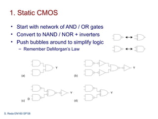
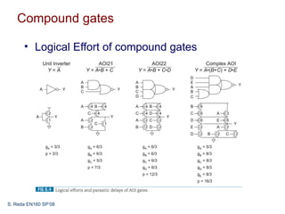
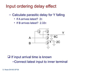
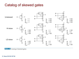
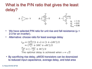
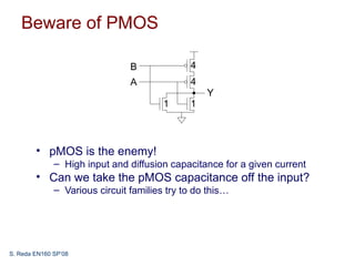
Design and Implementation of VLSI Systems
                  (EN01600)
        Lecture 19: Combinational Circuit Design (1/3)


S. Reda EN160 SP’08
Circuit Families


      1. Static CMOS
      2. Ratioed Circuits
      3. Cascode Voltage Switch Logic
      4. Dynamic Circuits
      5. Pass-transistor Circuits


S. Reda EN160 SP’08
1. Static CMOS
    • Start with network of AND / OR gates
    • Convert to NAND / NOR + inverters
    • Push bubbles around to simplify logic
          – Remember DeMorgan’s Law


                         Y                        Y

            (a)                    (b)


                               Y              Y

                  D
            (c)                    (d)


S. Reda EN160 SP’08
Compound gates

      • Logical Effort of compound gates


S. Reda EN160 SP’08
Input ordering delay effect
       – Calculate parasitic delay for Y falling
             • If A arrives latest? 2τ
             • If B arrives latest? 2.33τ


                                  2         2          Y
                         A                  2    6C

                         B                  2x    2C


      If input arrival time is known
        –Connect latest input to inner terminal

S. Reda EN160 SP’08
Asymmetric gates

    • Asymmetric gates favor one input over another
    • Ex: suppose input A of a NAND gate is most critical
          – Use smaller transistor on A (less capacitance)
          – Boost size of noncritical input
          – So total resistance is same
    • gA = 10/9
    • gB = 2
    • gavg = (gA + gB)/2 = 14/9
    • Asymmetric gate approaches g = 1 on critical input
    • But total logical effort goes up


S. Reda EN160 SP’08
Symmetric gates

      • Inputs can be made perfectly symmetric


                          2       2
                                       Y
                      A   1       1
                      B   1       1


S. Reda EN160 SP’08
Skewed gates
    • Skewed gates favor one transition over another
    • Ex: suppose rising output of inverter is most critical
          – Downsize noncritical nMOS transistor


    • Calculate logical effort by comparing to unskewed
      inverter with same effective resistance on that edge.
          – gu = 2.5 / 3 = 5/6
          – gd = 2.5 / 1.5 = 5/3


S. Reda EN160 SP’08
Hi- and Lo-Skew

      • Definition: Logical effort of a skewed gate for a
        particular transition is the ratio of the input
        capacitance of the skewed gate to the input
        capacitance of an unskewed inverter with equal drive
        for the same transition.

      • Skewed gates reduce size of noncritical transistors
            – HI-skew gates favor rising output (small nMOS)
            – LO-skew gates favor falling output (small pMOS)
      • Logical effort is smaller for favored direction
      • But larger for the other direction


S. Reda EN160 SP’08
Catalog of skewed gates


S. Reda EN160 SP’08
What is the P/N ratio that gives the least
   delay?


   • We have selected P/N ratio for unit rise and fall resistance (µ =
     2-3 for an inverter).
   • Alternative: choose ratio for least average delay


    • By sacrificing rise delay, pMOS transistors can be downsized
      to reduced input capacitance, average delay, and total area

S. Reda EN160 SP’08
Beware of PMOS

                                B             4
                                A             4
                                                  Y
                                        1     1


        • pMOS is the enemy!
              – High input and diffusion capacitance for a given current
        • Can we take the pMOS capacitance off the input?
              – Various circuit families try to do this…


S. Reda EN160 SP’08

Lecture19

  • 1.
    Design and Implementationof VLSI Systems (EN01600) Lecture 19: Combinational Circuit Design (1/3) S. Reda EN160 SP’08
  • 2.
    Circuit Families 1. Static CMOS 2. Ratioed Circuits 3. Cascode Voltage Switch Logic 4. Dynamic Circuits 5. Pass-transistor Circuits S. Reda EN160 SP’08
  • 3.
    1. Static CMOS • Start with network of AND / OR gates • Convert to NAND / NOR + inverters • Push bubbles around to simplify logic – Remember DeMorgan’s Law Y Y (a) (b) Y Y D (c) (d) S. Reda EN160 SP’08
  • 4.
    Compound gates • Logical Effort of compound gates S. Reda EN160 SP’08
  • 5.
    Input ordering delayeffect – Calculate parasitic delay for Y falling • If A arrives latest? 2τ • If B arrives latest? 2.33τ 2 2 Y A 2 6C B 2x 2C  If input arrival time is known –Connect latest input to inner terminal S. Reda EN160 SP’08
  • 6.
    Asymmetric gates • Asymmetric gates favor one input over another • Ex: suppose input A of a NAND gate is most critical – Use smaller transistor on A (less capacitance) – Boost size of noncritical input – So total resistance is same • gA = 10/9 • gB = 2 • gavg = (gA + gB)/2 = 14/9 • Asymmetric gate approaches g = 1 on critical input • But total logical effort goes up S. Reda EN160 SP’08
  • 7.
    Symmetric gates • Inputs can be made perfectly symmetric 2 2 Y A 1 1 B 1 1 S. Reda EN160 SP’08
  • 8.
    Skewed gates • Skewed gates favor one transition over another • Ex: suppose rising output of inverter is most critical – Downsize noncritical nMOS transistor • Calculate logical effort by comparing to unskewed inverter with same effective resistance on that edge. – gu = 2.5 / 3 = 5/6 – gd = 2.5 / 1.5 = 5/3 S. Reda EN160 SP’08
  • 9.
    Hi- and Lo-Skew • Definition: Logical effort of a skewed gate for a particular transition is the ratio of the input capacitance of the skewed gate to the input capacitance of an unskewed inverter with equal drive for the same transition. • Skewed gates reduce size of noncritical transistors – HI-skew gates favor rising output (small nMOS) – LO-skew gates favor falling output (small pMOS) • Logical effort is smaller for favored direction • But larger for the other direction S. Reda EN160 SP’08
  • 10.
    Catalog of skewedgates S. Reda EN160 SP’08
  • 11.
    What is theP/N ratio that gives the least delay? • We have selected P/N ratio for unit rise and fall resistance (µ = 2-3 for an inverter). • Alternative: choose ratio for least average delay • By sacrificing rise delay, pMOS transistors can be downsized to reduced input capacitance, average delay, and total area S. Reda EN160 SP’08
  • 12.
    Beware of PMOS B 4 A 4 Y 1 1 • pMOS is the enemy! – High input and diffusion capacitance for a given current • Can we take the pMOS capacitance off the input? – Various circuit families try to do this… S. Reda EN160 SP’08