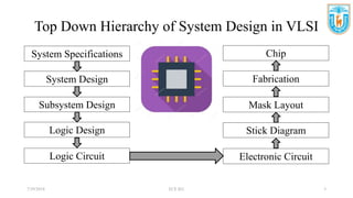
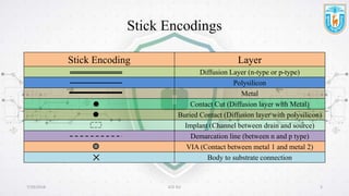
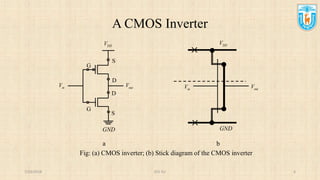
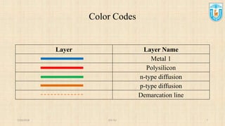
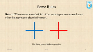
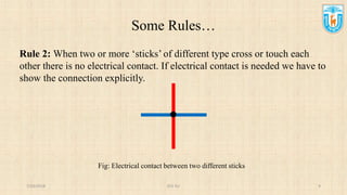
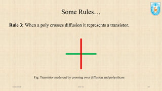
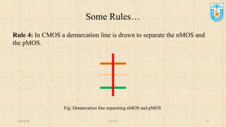
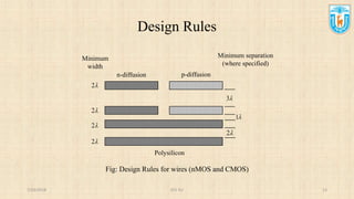
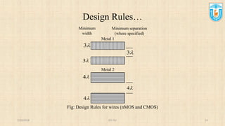
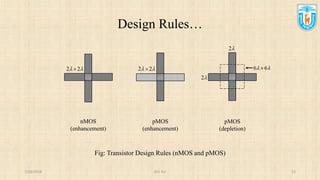
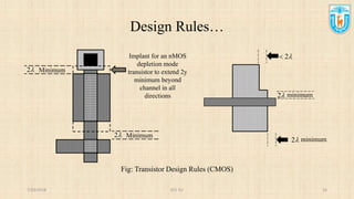
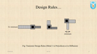
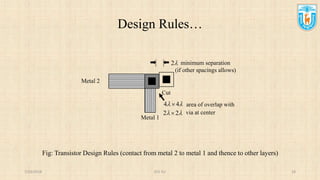
Stick Diagram
&
Lambda Based Design Rules
Presented by:
TAHSIN AL MAHI
Student ID: 140934
Year: 4 Term: I
ECE Discipline
Khulna University
Khulna
7/29/2018 ECE KU 1
7/29/2018 ECE KU 2
Presentation Outline
Top Down Hierarchy of System Design in VLSI
What is Stick Diagram
Stick Encodings
A CMOS inverter
Color Codes
Some Rules
What is Lambda Based Design Rule
Design Rules
7/29/2018 ECE KU 3
Top Down Hierarchy of System Design in VLSI
System Specifications
System Design
Subsystem Design
Logic Design
Logic Circuit Electronic Circuit
Stick Diagram
Mask Layout
Fabrication
Chip
7/29/2018 ECE KU 4
What is Stick Diagram?
o Stick diagram is a cartoon of a layout.
o Conveying layer information through the use of a color code or
monochrome encoding.
o Monochrome encodings are black and white lines.
D
S
G G
S
D
a b
Fig: (a) nMOS; (b) Stick Diagram of the nMOS
7/29/2018 ECE KU 5
Stick Encoding Layer
Diffusion Layer (n-type or p-type)
Polysilicon
Metal
Contact Cut (Diffusion layer with Metal)
Buried Contact (Diffusion layer with polysilicon)
Implant (Channel between drain and source)
Demarcation line (between n and p type)
VIA (Contact between metal 1 and metal 2)
Body to substrate connection
Stick Encodings
7/29/2018 ECE KU 6
A CMOS Inverter
D
S
G
S
D
G
a b
Fig: (a) CMOS inverter; (b) Stick diagram of the CMOS inverter
DDV
outVinV
GND
DDV
GND
inV outV
7/29/2018 ECE KU 7
Color Codes
Layer Layer Name
Metal 1
Polysilicon
n-type diffusion
p-type diffusion
Demarcation line
7/29/2018 ECE KU 8
Some Rules
Rule 1: When two or more ‘sticks’ of the same type cross or touch each
other that represents electrical contact.
Fig: Same type of sticks are crossing
7/29/2018 ECE KU 9
Some Rules…
Rule 2: When two or more ‘sticks’ of different type cross or touch each
other there is no electrical contact. If electrical contact is needed we have to
show the connection explicitly.
Fig: Electrical contact between two different sticks
7/29/2018 ECE KU 10
Some Rules…
Rule 3: When a poly crosses diffusion it represents a transistor.
Fig: Transistor made out by crossing over diffusion and polysilicon
7/29/2018 ECE KU 11
Some Rules…
Rule 4: In CMOS a demarcation line is drawn to separate the nMOS and
the pMOS.
Fig: Demarcation line separating nMOS and pMOS
7/29/2018 ECE KU 12
What is Lambda Based Design Rule
o Setting out mask dimensions along a size-independent way.
o Mead and Conway provided these rules.
o (Lambda) is a unit and can be of any value.
o According this rule line widths, separations and extensions are
expressed in terms of .
o Mask layout is designed according to Lambda Based Designed Rule.
o Nowadays, .


nm14
7/29/2018 ECE KU 13
Design Rules
Fig: Design Rules for wires (nMOS and CMOS)
3
2
2
2
2
1
2
n-diffusion p-diffusion
Minimum
width
Minimum separation
(where specified)
Polysilicon
7/29/2018 ECE KU 14
Design Rules…
Fig: Design Rules for wires (nMOS and CMOS)
3
Minimum
width
3
4
4
Minimum separation
(where specified)
4
Metal 2
Metal 1
3
7/29/2018 ECE KU 15
Design Rules…
Fig: Transistor Design Rules (nMOS and pMOS)
 22   22 
2
2
 66 
nMOS
(enhancement)
pMOS
(enhancement)
pMOS
(depletion)
7/29/2018 ECE KU 16
Design Rules…
2 Minimum
Implant for an nMOS
depletion mode
transistor to extend 2y
minimum beyond
channel in all
directions
2 Minimum
minimum
2
2 minimum
2
Fig: Transistor Design Rules (CMOS)
7/29/2018 ECE KU 17
Design Rules…
minimum3
2
minimum
Fig: Transistor Design Rules (Metal 1 to Polysilicon or to Diffusion)
7/29/2018 ECE KU 18
Design Rules…
Metal 2
Metal 1
2 minimum separation
(if other spacings allows)
Cut
 44  area of overlap with
 22  via at center
Fig: Transistor Design Rules (contact from metal 2 to metal 1 and thence to other layers)
7/29/2018 ECE KU 19
Reference
 Basic VLSI Design by Douglas A. Pucknell & Kamran Eshraghian
 Stick Diagrams, Maharishi Markandeshwar University, Haryana, India
7/29/2018 ECE KU 20
Any Questions?
7/29/2018 ECE KU 21

Stick Diagram and Lambda Based Design Rules

  • 1.
    Stick Diagram & Lambda BasedDesign Rules Presented by: TAHSIN AL MAHI Student ID: 140934 Year: 4 Term: I ECE Discipline Khulna University Khulna 7/29/2018 ECE KU 1
  • 2.
    7/29/2018 ECE KU2 Presentation Outline Top Down Hierarchy of System Design in VLSI What is Stick Diagram Stick Encodings A CMOS inverter Color Codes Some Rules What is Lambda Based Design Rule Design Rules
  • 3.
    7/29/2018 ECE KU3 Top Down Hierarchy of System Design in VLSI System Specifications System Design Subsystem Design Logic Design Logic Circuit Electronic Circuit Stick Diagram Mask Layout Fabrication Chip
  • 4.
    7/29/2018 ECE KU4 What is Stick Diagram? o Stick diagram is a cartoon of a layout. o Conveying layer information through the use of a color code or monochrome encoding. o Monochrome encodings are black and white lines. D S G G S D a b Fig: (a) nMOS; (b) Stick Diagram of the nMOS
  • 5.
    7/29/2018 ECE KU5 Stick Encoding Layer Diffusion Layer (n-type or p-type) Polysilicon Metal Contact Cut (Diffusion layer with Metal) Buried Contact (Diffusion layer with polysilicon) Implant (Channel between drain and source) Demarcation line (between n and p type) VIA (Contact between metal 1 and metal 2) Body to substrate connection Stick Encodings
  • 6.
    7/29/2018 ECE KU6 A CMOS Inverter D S G S D G a b Fig: (a) CMOS inverter; (b) Stick diagram of the CMOS inverter DDV outVinV GND DDV GND inV outV
  • 7.
    7/29/2018 ECE KU7 Color Codes Layer Layer Name Metal 1 Polysilicon n-type diffusion p-type diffusion Demarcation line
  • 8.
    7/29/2018 ECE KU8 Some Rules Rule 1: When two or more ‘sticks’ of the same type cross or touch each other that represents electrical contact. Fig: Same type of sticks are crossing
  • 9.
    7/29/2018 ECE KU9 Some Rules… Rule 2: When two or more ‘sticks’ of different type cross or touch each other there is no electrical contact. If electrical contact is needed we have to show the connection explicitly. Fig: Electrical contact between two different sticks
  • 10.
    7/29/2018 ECE KU10 Some Rules… Rule 3: When a poly crosses diffusion it represents a transistor. Fig: Transistor made out by crossing over diffusion and polysilicon
  • 11.
    7/29/2018 ECE KU11 Some Rules… Rule 4: In CMOS a demarcation line is drawn to separate the nMOS and the pMOS. Fig: Demarcation line separating nMOS and pMOS
  • 12.
    7/29/2018 ECE KU12 What is Lambda Based Design Rule o Setting out mask dimensions along a size-independent way. o Mead and Conway provided these rules. o (Lambda) is a unit and can be of any value. o According this rule line widths, separations and extensions are expressed in terms of . o Mask layout is designed according to Lambda Based Designed Rule. o Nowadays, .   nm14
  • 13.
    7/29/2018 ECE KU13 Design Rules Fig: Design Rules for wires (nMOS and CMOS) 3 2 2 2 2 1 2 n-diffusion p-diffusion Minimum width Minimum separation (where specified) Polysilicon
  • 14.
    7/29/2018 ECE KU14 Design Rules… Fig: Design Rules for wires (nMOS and CMOS) 3 Minimum width 3 4 4 Minimum separation (where specified) 4 Metal 2 Metal 1 3
  • 15.
    7/29/2018 ECE KU15 Design Rules… Fig: Transistor Design Rules (nMOS and pMOS)  22   22  2 2  66  nMOS (enhancement) pMOS (enhancement) pMOS (depletion)
  • 16.
    7/29/2018 ECE KU16 Design Rules… 2 Minimum Implant for an nMOS depletion mode transistor to extend 2y minimum beyond channel in all directions 2 Minimum minimum 2 2 minimum 2 Fig: Transistor Design Rules (CMOS)
  • 17.
    7/29/2018 ECE KU17 Design Rules… minimum3 2 minimum Fig: Transistor Design Rules (Metal 1 to Polysilicon or to Diffusion)
  • 18.
    7/29/2018 ECE KU18 Design Rules… Metal 2 Metal 1 2 minimum separation (if other spacings allows) Cut  44  area of overlap with  22  via at center Fig: Transistor Design Rules (contact from metal 2 to metal 1 and thence to other layers)
  • 19.
    7/29/2018 ECE KU19 Reference  Basic VLSI Design by Douglas A. Pucknell & Kamran Eshraghian  Stick Diagrams, Maharishi Markandeshwar University, Haryana, India
  • 20.
    7/29/2018 ECE KU20 Any Questions?
  • 21.