Downloaded 272 times
![EE415 VLSI Design
COMBINATIONAL
LOGIC DYNAMICS
[Adapted from Rabaey’s Digital Integrated Circuits, ©2002, J. Rabaey et al.]](https://image.slidesharecdn.com/lecture11combinationallogicdynamics-150625111023-lva1-app6891/85/Lecture11-combinational-logic-dynamics-1-320.jpg)
![EE415 VLSI Design
COMBINATIONAL
LOGIC DYNAMICS
[Adapted from Rabaey’s Digital Integrated Circuits, ©2002, J. Rabaey et al.]](https://image.slidesharecdn.com/lecture11combinationallogicdynamics-150625111023-lva1-app6891/75/Lecture11-combinational-logic-dynamics-1-2048.jpg)
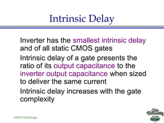
![EE415 VLSI Design
Pseudo-NMOS VTC
Noise margin low
is significantly
reduced comparing
to CMOS
0.0 0.5 1.0 1.5 2.0 2.5
0.0
0.5
1.0
1.5
2.0
2.5
3.0
Vin [V]
Vout[V]
W/Lp = 4
W/Lp = 2
W/Lp = 1
W/Lp = 0.25
W/Lp = 0.5
NL
Vin_low
Vin_highVin_low](https://image.slidesharecdn.com/lecture11combinationallogicdynamics-150625111023-lva1-app6891/85/Lecture11-combinational-logic-dynamics-31-320.jpg)
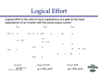
![EE415 VLSI Design
DCVSL Transient Response
0 0.2 0.4 0.6 0.8 1.0-0.5
0.5
1.5
2.5
Time [ns]
Voltage[V]
A B
A B
A,B
A,B
DCVSL transient response of AND/NAND gate](https://image.slidesharecdn.com/lecture11combinationallogicdynamics-150625111023-lva1-app6891/85/Lecture11-combinational-logic-dynamics-36-320.jpg)
![EE415 VLSI Design
NMOS-Only Logic
VDD
In
Out
x
0.5µm/0.25µm
0.5µm/0.25µm
1.5µm/0.25µm
0 0.5 1 1.5 2
0.0
1.0
2.0
3.0
Time [ns]
Voltage[V]
x
Out
In](https://image.slidesharecdn.com/lecture11combinationallogicdynamics-150625111023-lva1-app6891/85/Lecture11-combinational-logic-dynamics-39-320.jpg)
![EE415 VLSI Design
Restorer Transistor Sizing
0 100 200 300 400 500
0.0
1.0
2.0
W/Lr
=1.0/0.25 W /Lr
=1.25/0.25
W /Lr
=1.50/0.25
W /Lr
=1.75/0.25
Voltage[V]
Time [ps]
3.0
•Level restoring transistor
cannot be too strong otherwise
it will prevent output from
reaching VDD value
•Upper limit on restorer size
•Pass-transistor pull-down
can have several transistors in
stack](https://image.slidesharecdn.com/lecture11combinationallogicdynamics-150625111023-lva1-app6891/85/Lecture11-combinational-logic-dynamics-42-320.jpg)
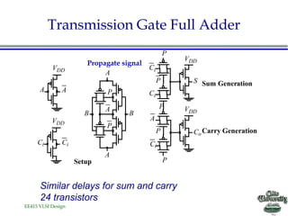

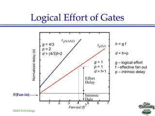
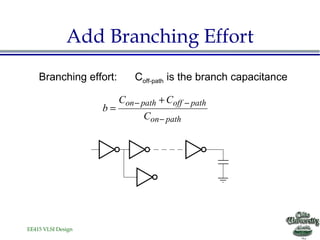
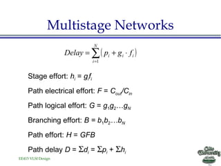
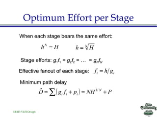
- The document discusses various techniques for designing fast complex logic gates in VLSI circuits. - Two transistor sizing techniques are presented: progressive transistor sizing and transistor ordering to reduce signal delay. - Alternative logic structures, buffer insertion, and reducing voltage swing are additional techniques described. - The concept of logical effort is introduced as a way to optimize logic paths for speed based on the topology rather than transistor sizing.