Fan-in and Fan-out.ppt
•
0 likes•1,577 views
Fan in and Fan out related to vlsi design basic circuit concepts. This will be used for IC design process. By using such key methods, the performance of the circuit in IC will be improved in a better manner.
Report
Share
Report
Share

Recommended
Pass Transistor Logic
This presentation discusses the basics of Pass Transistor Logic, its advantages, limitation and finally implementation of Boolean functions/Combinational Logic circuits using Pass Transistor Logic.
4. single stage amplifier
The document discusses single-stage amplifiers, specifically common source amplifiers. It covers the basics of common source amplifiers and different types of loads that can be used, including resistive loads. It analyzes the gain of common source amplifiers with resistive loads using both small-signal and large-signal models, taking into account effects such as channel length modulation. The analysis shows tradeoffs between gain, bandwidth, and voltage swing that must be considered in amplifier design.
Vlsi ppt priyanka
In this presentation of mine, a basic Design approach of VLSI has been explained. The ppt explains the market level of VLSI and also the fabrication process and also its various applications. An integration of various switches, gates, etc on Ic's has also been showcased in the same.
Combinational Logic
Combinational Logic
Pass Transistors
Transmission Gates
Pseudo nMOS Logic
Tri-state Logic
Dynamic Logic
Domino Logic
Dynamic logic circuits
This document discusses dynamic logic circuits. It notes that dynamic logic circuits offer advantages over static logic circuits by temporarily storing charge in parasitic capacitances rather than relying on steady-state behavior. Dynamic logic circuits require periodic clock signals to control charge refreshing and allow for simple sequential circuits with memory. They can implement logic in smaller areas and thus consume less power than static logic. The document then discusses several examples of dynamic logic circuits like dynamic CMOS TG logic, domino CMOS logic, NORA logic, and their operating principles. It also covers issues like charge leakage and charge sharing that need to be addressed in dynamic logic circuits.
VLSI Technology Trends
This document provides an overview of VLSI technology trends over time. It discusses how Moore's Law has been sustained through transistor scaling down to the nanometer level enabled by various techniques like strained silicon, high-k dielectrics, metal gates, SOI, multi-gate transistors like FinFETs. It outlines the evolution from bipolar junction transistors to MOSFETs to integrated circuits. Short channel effects posed challenges to scaling which were addressed through new device architectures in the second generation of scaling.
Packaging of vlsi devices
This document discusses package design considerations and types of semiconductor packages. It covers key factors in package design like the number of terminals, electrical, thermal, and reliability requirements. The main package types discussed are through-hole packages like DIP and QFP, and surface mount packages like SOP, PLCC, and LCCC. Through-hole packages use precision holes drilled through the board while surface mount packages solder directly to the board surface.
ASIC DESIGN : PLACEMENT
This document discusses ASIC placement, which involves assigning exact locations to circuit components within a chip's core area. The goals of placement are to minimize the total interconnect length and costs while meeting timing requirements. It describes two main placement techniques - global placement, which groups cells to minimize interconnect between groups, and detailed placement, which further optimizes placement objectives. The document outlines various placement algorithms, goals, and trends like mixed-size placement and whitespace distribution to improve routability and performance.
Interconnect timing model
This document discusses different interconnect timing models used to model delays caused by interconnects in integrated circuits. It describes lumped capacitor, transmission line, lumped RC, Elmore delay, distributed RC, and RLC models. The lumped capacitor and transmission line models treat interconnects as either purely capacitive or propagating waves, while the lumped RC, distributed RC, and RLC models account for resistive and inductive effects at higher frequencies. The Elmore delay model provides a simplified yet accurate way to calculate delays in RC networks. Overall, the choice of timing model depends on factors like the operating frequency and interconnect geometry.
Analog to digital converter
This document provides an overview of analog to digital converters (ADCs). It discusses the basic process of converting a continuous analog signal to discrete digital values. It then describes several common types of ADCs - successive approximation ADCs, dual slope ADCs, flash ADCs, and pipeline ADCs. For each type, it provides details on how the conversion process works, as well as advantages and disadvantages. It explains key steps and components involved, such as sampling and holding, quantizing, encoding, comparators and resistors. The document serves to introduce the fundamental concept and major implementation techniques for analog to digital conversion.
CMOS TG
The document summarizes the operation of a CMOS transmission gate (TG). A TG consists of a parallel nMOS and pMOS transistor that act as a bidirectional switch controlled by complementary signals on the gates. When the control input is high, both transistors are off and the TG acts as a high impedance state. When the control input is low, one transistor is on providing a conduction path from input to output. The document further analyzes the DC characteristics of a TG under different bias conditions.
Packaging of vlsi devices
This document discusses packaging considerations for VLSI devices. It covers package types like through-hole packages, surface-mounted packages, flip chip packages, and chip-scale packages. Key package design considerations include the number of terminals, electrical design to minimize signal degradation, thermal design to dissipate heat, reliability over temperature cycles, and testability to ensure quality. The ideal package is compact with low-inductance connections to transfer heat efficiently while withstanding stresses.
VLSI Power Reduction
Semiconductor engineering is becoming more dynamic fiels since the technology scaling is taking place. Power reduction techniques are lucrative solutions to the performance, area and power trade off. Therefore Power reduction of VLSI designs are critical.
VLSI routing
Routing in Integrated circuits is an important task which requires extreme care while placing the modules and circuits and connecting them with each other.
IC Technology
This document discusses integrated circuit technology. It begins with an overview of the IC market breakdown by sector. It then discusses advantages of ICs such as smaller size, higher speed, lower power consumption compared to discrete components. The document provides a history of important IC inventions from 1904 to the present. It also discusses transistor scaling that has allowed achieving more complex ICs through reduced dimensions over time. Finally, it covers different IC design styles such as full custom, standard cell, gate array, and FPGA and their tradeoffs in terms of performance, cost, area, and time-to-market.
Pulse shaping
In electronics and telecommunications, pulse shaping is the process of changing the waveform of transmitted pulses.
Two cavity klystron
A Klystron is a vacuum tube that can be used either as a generator or as an amplifier or as an oscillator, at microwave frequencies.The Klystron is a linear beam device; that is, the electron flow is in a straight line focused by an axial magnetic field.
Overview of digital design with Verilog HDL
Evolution of Computer Aided Digital Design
Emergence of HDLs
Typical Design flow
Importance of HDLs
Popularity of Verilog HDL
Trends in HDLs
Double Patterning (4/2 update)
This document discusses double patterning lithography techniques. It introduces how optical lithography is approaching its limits and double patterning is needed for smaller feature sizes. It describes the double patterning process and challenges including feature distortion and decreased yield. The document outlines techniques for polygon cutting, priority search trees, and decomposing conflict graphs into tri-connected components to solve the layout splitting problem. Experimental results on test cases including a 320k polygon design show the method achieves 3-10x speedup.
FPGA
This document discusses field programmable gate arrays (FPGAs). It begins by describing FPGA basics and architecture, including configurable logic blocks (CLBs), I/O blocks, and switch matrices. It then discusses FPGA advantages such as low cost, fast prototyping, and reusability. The document also covers FPGA process technologies including SRAM, antifuse, and EPROM/EEPROM/Flash. It provides details on FPGA architectures, logic elements, routing, memory blocks, and examples of Xilinx FPGAs.
Fpga architectures and applications
FPGAs can be programmed after manufacturing to implement custom logic functions. They contain programmable logic blocks and interconnects that can be configured to create custom circuits. FPGAs provide flexibility compared to ASICs but have higher per-unit costs. The FPGA architecture consists of configurable logic blocks, programmable interconnects, and I/O blocks. Configurable logic blocks contain LUTs that implement logic functions. Programmable interconnects connect the logic blocks, and I/O blocks interface with external components. FPGAs are commonly used for prototyping, emulation, parallel computing, and other applications that require customizable hardware.
faults in digital systems
Faults can occur in digital circuits due to processing errors, material defects, time-dependent failures, or packaging issues. A fault is a physical defect, an error is the manifestation of a fault causing incorrect outputs, and a failure occurs when a circuit deviates from its specified behavior due to an error. The single stuck-at fault model assumes a line is permanently stuck at 0 or 1, and is commonly used due to its simplicity and ability to model many defects. Bridging faults occur when two lines are accidentally connected, and can be modeled as ANDing or ORing the signals. Feedback bridging can cause circuits to oscillate or behave asynchronously under certain input conditions.
Asic design
An application-specific IC (ASIC) can be either a digital or an analog circuit. As their name implies, ASICs are not reconfigurable; they perform only one specific function. For example, a speed controller IC for a remote control car is hard-wired to do one job and could never become a microprocessor. An ASIC does not contain any ability to follow alternate instructions.
digital logic_families
Digital logic families classify integrated circuits by their circuit technology. A logic family consists of chips that perform logic functions like AND and OR with similar input/output characteristics. Popular families include TTL, ECL, MOS, and CMOS. CMOS uses fewer transistors than other families for inversion and is known for low power. Logic levels and noise margins define input and output voltage thresholds. Transition times and capacitive loading affect a circuit's propagation delay.
Low Power Techniques
This document discusses various low power techniques for integrated circuits. It begins by describing the increasing challenges of power consumption as device densities and clock frequencies increase while supply voltages and threshold voltages decrease. It then discusses different types of power consumption, including dynamic power, static power, leakage power from different sources, and how they can be reduced. The document covers many low power design techniques like multi-threshold CMOS, clock gating, multi-voltage, DVFS, and more. It discusses the evolution of these techniques and challenges in their implementation like timing issues, level shifters, and floorplanning for multi-voltage designs.
3673 mosfet
The document discusses the MOS transistor and its operation. It begins by describing the components and structure of the MOS transistor, including the polysilicon gate, aluminum contacts, and silicon dioxide layer. It then discusses the energy band diagrams and how applying different gate voltages results in accumulation, depletion, or inversion at the surface. The document also covers the threshold voltage, its dependence on factors like doping and oxide thickness, and its impact on MOSFET operation. It concludes by deriving the MOSFET drain current equation using the gradual channel approximation approach.
Second order effects
The document discusses four topics related to transistors:
1. Threshold voltage is the minimum gate voltage needed to create a conducting path between source and drain, and depends on oxide thickness, temperature, and random dopant fluctuations.
2. Latchup refers to a short circuit formed between power and ground rails in an integrated circuit, caused by interaction between parasitic bipolar transistors.
3. Electromigration is the forced movement of metal ions due to an electric field, with atoms traveling toward the positive conductor end and vacancies toward the negative end.
4. Mobility degradation occurs due to lateral and vertical electric fields scattering carriers, reducing surface mobility as channel lengths shrink.
LBC Presentation May 7, 2011(COMP04)
This document outlines an agenda for a seminar on structured cabling systems. The agenda includes an overview of structured cabling system subsystems and transmission line diagrams. It also covers horizontal subsystem design, including the components, types of horizontal cabling, and a sample design. Finally, it discusses cabling installation and practical applications. The presentation slides provide additional details on topics like the structured cabling subsystem architecture, transmission line diagrams, cable and connector types for different subsystem levels, and horizontal subsystem design considerations.
Ly3620482052
International Journal of Engineering Research and Applications (IJERA) aims to cover the latest outstanding developments in the field of all Engineering Technologies & science.
International Journal of Engineering Research and Applications (IJERA) is a team of researchers not publication services or private publications running the journals for monetary benefits, we are association of scientists and academia who focus only on supporting authors who want to publish their work. The articles published in our journal can be accessed online, all the articles will be archived for real time access.
Our journal system primarily aims to bring out the research talent and the works done by sciaentists, academia, engineers, practitioners, scholars, post graduate students of engineering and science. This journal aims to cover the scientific research in a broader sense and not publishing a niche area of research facilitating researchers from various verticals to publish their papers. It is also aimed to provide a platform for the researchers to publish in a shorter of time, enabling them to continue further All articles published are freely available to scientific researchers in the Government agencies,educators and the general public. We are taking serious efforts to promote our journal across the globe in various ways, we are sure that our journal will act as a scientific platform for all researchers to publish their works online.
More Related Content
What's hot
ASIC DESIGN : PLACEMENT
This document discusses ASIC placement, which involves assigning exact locations to circuit components within a chip's core area. The goals of placement are to minimize the total interconnect length and costs while meeting timing requirements. It describes two main placement techniques - global placement, which groups cells to minimize interconnect between groups, and detailed placement, which further optimizes placement objectives. The document outlines various placement algorithms, goals, and trends like mixed-size placement and whitespace distribution to improve routability and performance.
Interconnect timing model
This document discusses different interconnect timing models used to model delays caused by interconnects in integrated circuits. It describes lumped capacitor, transmission line, lumped RC, Elmore delay, distributed RC, and RLC models. The lumped capacitor and transmission line models treat interconnects as either purely capacitive or propagating waves, while the lumped RC, distributed RC, and RLC models account for resistive and inductive effects at higher frequencies. The Elmore delay model provides a simplified yet accurate way to calculate delays in RC networks. Overall, the choice of timing model depends on factors like the operating frequency and interconnect geometry.
Analog to digital converter
This document provides an overview of analog to digital converters (ADCs). It discusses the basic process of converting a continuous analog signal to discrete digital values. It then describes several common types of ADCs - successive approximation ADCs, dual slope ADCs, flash ADCs, and pipeline ADCs. For each type, it provides details on how the conversion process works, as well as advantages and disadvantages. It explains key steps and components involved, such as sampling and holding, quantizing, encoding, comparators and resistors. The document serves to introduce the fundamental concept and major implementation techniques for analog to digital conversion.
CMOS TG
The document summarizes the operation of a CMOS transmission gate (TG). A TG consists of a parallel nMOS and pMOS transistor that act as a bidirectional switch controlled by complementary signals on the gates. When the control input is high, both transistors are off and the TG acts as a high impedance state. When the control input is low, one transistor is on providing a conduction path from input to output. The document further analyzes the DC characteristics of a TG under different bias conditions.
Packaging of vlsi devices
This document discusses packaging considerations for VLSI devices. It covers package types like through-hole packages, surface-mounted packages, flip chip packages, and chip-scale packages. Key package design considerations include the number of terminals, electrical design to minimize signal degradation, thermal design to dissipate heat, reliability over temperature cycles, and testability to ensure quality. The ideal package is compact with low-inductance connections to transfer heat efficiently while withstanding stresses.
VLSI Power Reduction
Semiconductor engineering is becoming more dynamic fiels since the technology scaling is taking place. Power reduction techniques are lucrative solutions to the performance, area and power trade off. Therefore Power reduction of VLSI designs are critical.
VLSI routing
Routing in Integrated circuits is an important task which requires extreme care while placing the modules and circuits and connecting them with each other.
IC Technology
This document discusses integrated circuit technology. It begins with an overview of the IC market breakdown by sector. It then discusses advantages of ICs such as smaller size, higher speed, lower power consumption compared to discrete components. The document provides a history of important IC inventions from 1904 to the present. It also discusses transistor scaling that has allowed achieving more complex ICs through reduced dimensions over time. Finally, it covers different IC design styles such as full custom, standard cell, gate array, and FPGA and their tradeoffs in terms of performance, cost, area, and time-to-market.
Pulse shaping
In electronics and telecommunications, pulse shaping is the process of changing the waveform of transmitted pulses.
Two cavity klystron
A Klystron is a vacuum tube that can be used either as a generator or as an amplifier or as an oscillator, at microwave frequencies.The Klystron is a linear beam device; that is, the electron flow is in a straight line focused by an axial magnetic field.
Overview of digital design with Verilog HDL
Evolution of Computer Aided Digital Design
Emergence of HDLs
Typical Design flow
Importance of HDLs
Popularity of Verilog HDL
Trends in HDLs
Double Patterning (4/2 update)
This document discusses double patterning lithography techniques. It introduces how optical lithography is approaching its limits and double patterning is needed for smaller feature sizes. It describes the double patterning process and challenges including feature distortion and decreased yield. The document outlines techniques for polygon cutting, priority search trees, and decomposing conflict graphs into tri-connected components to solve the layout splitting problem. Experimental results on test cases including a 320k polygon design show the method achieves 3-10x speedup.
FPGA
This document discusses field programmable gate arrays (FPGAs). It begins by describing FPGA basics and architecture, including configurable logic blocks (CLBs), I/O blocks, and switch matrices. It then discusses FPGA advantages such as low cost, fast prototyping, and reusability. The document also covers FPGA process technologies including SRAM, antifuse, and EPROM/EEPROM/Flash. It provides details on FPGA architectures, logic elements, routing, memory blocks, and examples of Xilinx FPGAs.
Fpga architectures and applications
FPGAs can be programmed after manufacturing to implement custom logic functions. They contain programmable logic blocks and interconnects that can be configured to create custom circuits. FPGAs provide flexibility compared to ASICs but have higher per-unit costs. The FPGA architecture consists of configurable logic blocks, programmable interconnects, and I/O blocks. Configurable logic blocks contain LUTs that implement logic functions. Programmable interconnects connect the logic blocks, and I/O blocks interface with external components. FPGAs are commonly used for prototyping, emulation, parallel computing, and other applications that require customizable hardware.
faults in digital systems
Faults can occur in digital circuits due to processing errors, material defects, time-dependent failures, or packaging issues. A fault is a physical defect, an error is the manifestation of a fault causing incorrect outputs, and a failure occurs when a circuit deviates from its specified behavior due to an error. The single stuck-at fault model assumes a line is permanently stuck at 0 or 1, and is commonly used due to its simplicity and ability to model many defects. Bridging faults occur when two lines are accidentally connected, and can be modeled as ANDing or ORing the signals. Feedback bridging can cause circuits to oscillate or behave asynchronously under certain input conditions.
Asic design
An application-specific IC (ASIC) can be either a digital or an analog circuit. As their name implies, ASICs are not reconfigurable; they perform only one specific function. For example, a speed controller IC for a remote control car is hard-wired to do one job and could never become a microprocessor. An ASIC does not contain any ability to follow alternate instructions.
digital logic_families
Digital logic families classify integrated circuits by their circuit technology. A logic family consists of chips that perform logic functions like AND and OR with similar input/output characteristics. Popular families include TTL, ECL, MOS, and CMOS. CMOS uses fewer transistors than other families for inversion and is known for low power. Logic levels and noise margins define input and output voltage thresholds. Transition times and capacitive loading affect a circuit's propagation delay.
Low Power Techniques
This document discusses various low power techniques for integrated circuits. It begins by describing the increasing challenges of power consumption as device densities and clock frequencies increase while supply voltages and threshold voltages decrease. It then discusses different types of power consumption, including dynamic power, static power, leakage power from different sources, and how they can be reduced. The document covers many low power design techniques like multi-threshold CMOS, clock gating, multi-voltage, DVFS, and more. It discusses the evolution of these techniques and challenges in their implementation like timing issues, level shifters, and floorplanning for multi-voltage designs.
3673 mosfet
The document discusses the MOS transistor and its operation. It begins by describing the components and structure of the MOS transistor, including the polysilicon gate, aluminum contacts, and silicon dioxide layer. It then discusses the energy band diagrams and how applying different gate voltages results in accumulation, depletion, or inversion at the surface. The document also covers the threshold voltage, its dependence on factors like doping and oxide thickness, and its impact on MOSFET operation. It concludes by deriving the MOSFET drain current equation using the gradual channel approximation approach.
Second order effects
The document discusses four topics related to transistors:
1. Threshold voltage is the minimum gate voltage needed to create a conducting path between source and drain, and depends on oxide thickness, temperature, and random dopant fluctuations.
2. Latchup refers to a short circuit formed between power and ground rails in an integrated circuit, caused by interaction between parasitic bipolar transistors.
3. Electromigration is the forced movement of metal ions due to an electric field, with atoms traveling toward the positive conductor end and vacancies toward the negative end.
4. Mobility degradation occurs due to lateral and vertical electric fields scattering carriers, reducing surface mobility as channel lengths shrink.
What's hot (20)
Similar to Fan-in and Fan-out.ppt
LBC Presentation May 7, 2011(COMP04)
This document outlines an agenda for a seminar on structured cabling systems. The agenda includes an overview of structured cabling system subsystems and transmission line diagrams. It also covers horizontal subsystem design, including the components, types of horizontal cabling, and a sample design. Finally, it discusses cabling installation and practical applications. The presentation slides provide additional details on topics like the structured cabling subsystem architecture, transmission line diagrams, cable and connector types for different subsystem levels, and horizontal subsystem design considerations.
Ly3620482052
International Journal of Engineering Research and Applications (IJERA) aims to cover the latest outstanding developments in the field of all Engineering Technologies & science.
International Journal of Engineering Research and Applications (IJERA) is a team of researchers not publication services or private publications running the journals for monetary benefits, we are association of scientists and academia who focus only on supporting authors who want to publish their work. The articles published in our journal can be accessed online, all the articles will be archived for real time access.
Our journal system primarily aims to bring out the research talent and the works done by sciaentists, academia, engineers, practitioners, scholars, post graduate students of engineering and science. This journal aims to cover the scientific research in a broader sense and not publishing a niche area of research facilitating researchers from various verticals to publish their papers. It is also aimed to provide a platform for the researchers to publish in a shorter of time, enabling them to continue further All articles published are freely available to scientific researchers in the Government agencies,educators and the general public. We are taking serious efforts to promote our journal across the globe in various ways, we are sure that our journal will act as a scientific platform for all researchers to publish their works online.
Chpt 4 (presentation 2)
To learn the definition of Static CMOS Logic Circuit, truly know how to apply in use of the function of Static CMOS Logic Circuit in life.
Layout design
Lecture 4
18-322 Fall 2003
Textbook: Design Methodology Insert A
[Portions adapted from J. P. Uyemura “Introduction to VLSI Circuits and Systems”, Wiley 2001.]
Design & Performance Analysis of DG-MOSFET for Reduction of Short Channel Eff...
An aggressive scaling of conventional MOSFETs channel length reduces below 100nm and gate oxide thickness below 3nm to improved performance and packaging density. Due to this scaling short channel effect (SCEs) like threshold voltage, Subthreshold slope, ON current and OFF current plays a major role in determining the performance of scaled devices. The double gate (DG) MOSFETS are electro-statically superior to a single gate (SG) MOSFET and allows for additional gate length scaling. Simulation work on both devices has been carried out and presented in paper. The comparative study had been carried out for threshold voltage (VT), Subthreshold slope (Sub VT), ION and IOFF Current. It is observed that DG MOSFET provide good control on leakage current over conventional Bulk (Single Gate) MOSFET. The VT (Threshold Voltage) is 2.7 times greater than & ION of DG MOSFET is 2.2 times smaller than the conventional Bulk (Single Gate) MOSFET.
2m bp filter yu1 lm
This document describes the design of a band pass filter for the 2 meter amateur radio band with low insertion loss. The filter uses surface mount capacitor and inductor components to create a band pass response that attenuates signals outside of the 2m band, including FM radio and TV bands, by at least 40 dB. It is intended to improve the performance of the author's 2m software defined radio receiver by reducing overload from out of band signals. Construction details are provided for building the filter using inexpensive surface mount components on a double sided printed circuit board.
FUNDAMENTALS OF HIGH SPEED DESIGN.pdf
This document discusses fundamentals of high speed PCB design. It covers topics like what constitutes a high speed design, signal propagation, transmission lines, impedance matching, stackup selection, routing guidelines, and do's/don'ts. Key aspects addressed include maintaining consistent impedance, minimizing reflections, controlling skew, ensuring return current paths, and using proper termination and vias. Designing high speed circuits requires attention to these factors to optimize signal integrity.
CMOS Topic 6 -_designing_combinational_logic_circuits
This document discusses designing combinational logic circuits using static complementary CMOS design. It explains how to construct static CMOS circuits for logic gates like NAND and NOR by using pull-up and pull-down networks of PMOS and NMOS transistors respectively. Issues related to pass-transistor design like noise margins and static power consumption are also covered. The document provides details on implementing various logic functions using pass-transistor logic and differential pass-transistor logic. It discusses solutions to overcome the disadvantages of pass-transistor logic like level restoration and use of multiple threshold transistors.
Bo q supply of two steel modular tanks - galvanized finish for kadugli urba...
This document is a bill of quantities for supplying and installing two modular steel tanks for water storage in Kadugli, Sudan. It specifies the requirements for the tanks, including dimensions, materials, coatings, and plumbing features. It also outlines responsibilities for supplying labor, transport, and documentation. The supplier must provide structural analysis, shop drawings, installation supervision and spare parts. The client is responsible for the foundation, casual labor, and facilitating the supplier's work in Sudan. The completion period is two months after the tanks arrive in Sudan.
City gas distribution- Complete Overview
This document provides an overview of city gas distribution systems. It discusses what city gas distribution is, the basic concepts of distribution systems including developing pipeline networks and maintaining different pressure levels. It outlines the key steps in designing distribution systems such as demand estimation, network design, and route surveys. The document also covers system components including city gate stations, pipelines, regulating stations, meters, and CNG stations. It concludes by discussing applicable codes, standards, and regulations for city gas distribution.
P1121110526
This document discusses surround gate MOSFETs as an approach to reduce short channel effects in transistors. It begins with an overview of MOSFET operation and Moore's Law. It then discusses the motivation to find alternatives to planar transistors as scaling limits are approached. Short channel effects in bulk MOSFETs are introduced as a major barrier to scaling. The document reviews SOI and multi-gate transistor technologies, such as double gate, tri-gate, and gate-all-around designs, as ways to better control the channel and reduce short channel effects. A new dual-material surround gate structure is proposed and its potential to further suppress short channel effects through gate material engineering is explained. Two-dimensional modeling of the new structure
ComNet FDX70EAM1 Data Sheet
Buy the ComNet FDX70EAM1 at JMAC Supply.
http://www.jmac.com/ComNet_FDX70EAM1_p/comnet-fdx70eam1.htm?=slideshare
ComNet FDX72M1SHR Data Sheet
Buy the ComNet FDX72M1SHR at JMAC Supply.
http://www.jmac.com/ComNet_FDX72M1SHR_p/comnet-fdx72m1shr.htm?=slideshare
Metal Insulator Semiconductor devices
The document discusses MOSFET transistors. It describes their basic structure as having a gate, source and drain, with the gate separated from the semiconductor material by an insulating oxide layer. MOSFETs can be either n-channel or p-channel and either enhancement or depletion mode. Their operation depends on the voltage applied to the gate, which controls the flow of current between the source and drain. MOSFETs are widely used in applications like microprocessors and memories due to their low cost, small size and low power consumption. The CMOS inverter circuit is also discussed, which uses complementary n-channel and p-channel MOSFETs.
MOSFET_Scaling0803.ppt
MOSFET scaling involves decreasing the transistor length (L) and voltage (VDD) over generations according to scaling factors (a) and (b), respectively. To maintain device operation, the doping concentration must increase by a factor of a. As lengths decrease, tunneling current increases due to highly doped source/drain junctions and thin gate oxides. Using high-k dielectrics allows a physically thicker gate oxide to reduce tunneling. FinFET structures improve channel control and decrease spreading resistance issues compared to planar MOSFETs. Future devices will focus on techniques like SOI and raised source/drains to further scaling limits.
MOSFET_Scaling5012.ppt
MOSFET scaling involves decreasing the transistor length (L) and voltage (VDD) over generations according to scaling factors (a) and (b), respectively. To maintain device operation, the doping concentration must increase by a factor of a. As lengths decrease, tunneling current increases due to highly doped source/drain junctions and thin gate oxides. Using high-k dielectrics and fully depleted devices like FinFETs can help mitigate these tunneling issues to allow continued scaling. Future devices will focus on improving subthreshold current, spreading resistance, and multi-gate control to enable further miniaturization.
BlueOptics Bo66jxx660d 10gbase cwdm xfp transceiver 1271nm 1451nm 60 km singl...
BlueOptics Bo66jxx660d 10gbase cwdm xfp transceiver 1271nm 1451nm 60 km singlemode lc duplex 10 gigabit
HYC Co., Ltd 2019 New Product Manual
HYC Co., Ltd, 2019 new products is including LC push-pull connector, lc polarity revisable uniboot connector,lc duplex sll connector, lc internal shutter adapter,mpo connector,mpo adapter,1U/2U/4U rack mount enclosure for data center solutions, plc splitter, aawg module, awg cwdm4 designed for 40G/100G active optical module, wdm lgx module, CCWDM module, Mini WDM, AOC series, SC optical reflector, FTTH box, MEMS optical switch, MCS module, and so on. Get more: http://www.hyc-system.com
HYC Co., Ltd 2019 New Product Manual
HYC is a manufacturer of fiber optic connectivity products including push-pull connectors, duplex connectors, MPO connectors, adapters, splitters, wavelength division multiplexing devices, and other solutions for data centers and fiber to the home applications. Their products are compliant with relevant standards and have features such as low insertion loss, compact size, customizable logos, and polarity switching capabilities.
VLSI D PPT.pdf
This document discusses MOSFET and BiCMOS technologies. It begins by introducing the basic electrical properties of MOS and BiCMOS circuits, including current-voltage relationships and threshold voltages. It then discusses MOS transistor regions of operation and how a channel is formed. The document also covers the fabrication processes for monolithic ICs such as oxidation, photolithography, diffusion, and metallization. Finally, it discusses BiCMOS inverters and compares the characteristics and advantages of bipolar, CMOS, and BiCMOS technologies.
Similar to Fan-in and Fan-out.ppt (20)
Design & Performance Analysis of DG-MOSFET for Reduction of Short Channel Eff...
Design & Performance Analysis of DG-MOSFET for Reduction of Short Channel Eff...
CMOS Topic 6 -_designing_combinational_logic_circuits
CMOS Topic 6 -_designing_combinational_logic_circuits
Bo q supply of two steel modular tanks - galvanized finish for kadugli urba...
Bo q supply of two steel modular tanks - galvanized finish for kadugli urba...
BlueOptics Bo66jxx660d 10gbase cwdm xfp transceiver 1271nm 1451nm 60 km singl...
BlueOptics Bo66jxx660d 10gbase cwdm xfp transceiver 1271nm 1451nm 60 km singl...
Recently uploaded
Your Skill Boost Masterclass: Strategies for Effective Upskilling
Your Skill Boost Masterclass: Strategies for Effective UpskillingExcellence Foundation for South Sudan
Strategies for Effective Upskilling is a presentation by Chinwendu Peace in a Your Skill Boost Masterclass organisation by the Excellence Foundation for South Sudan on 08th and 09th June 2024 from 1 PM to 3 PM on each day.Types of Herbal Cosmetics its standardization.
Physiology and chemistry of skin and pigmentation, hairs, scalp, lips and nail, Cleansing cream, Lotions, Face powders, Face packs, Lipsticks, Bath products, soaps and baby product,
Preparation and standardization of the following : Tonic, Bleaches, Dentifrices and Mouth washes & Tooth Pastes, Cosmetics for Nails.
A Strategic Approach: GenAI in Education
Artificial Intelligence (AI) technologies such as Generative AI, Image Generators and Large Language Models have had a dramatic impact on teaching, learning and assessment over the past 18 months. The most immediate threat AI posed was to Academic Integrity with Higher Education Institutes (HEIs) focusing their efforts on combating the use of GenAI in assessment. Guidelines were developed for staff and students, policies put in place too. Innovative educators have forged paths in the use of Generative AI for teaching, learning and assessments leading to pockets of transformation springing up across HEIs, often with little or no top-down guidance, support or direction.
This Gasta posits a strategic approach to integrating AI into HEIs to prepare staff, students and the curriculum for an evolving world and workplace. We will highlight the advantages of working with these technologies beyond the realm of teaching, learning and assessment by considering prompt engineering skills, industry impact, curriculum changes, and the need for staff upskilling. In contrast, not engaging strategically with Generative AI poses risks, including falling behind peers, missed opportunities and failing to ensure our graduates remain employable. The rapid evolution of AI technologies necessitates a proactive and strategic approach if we are to remain relevant.
ANATOMY AND BIOMECHANICS OF HIP JOINT.pdf
it describes the bony anatomy including the femoral head , acetabulum, labrum . also discusses the capsule , ligaments . muscle that act on the hip joint and the range of motion are outlined. factors affecting hip joint stability and weight transmission through the joint are summarized.
How to Build a Module in Odoo 17 Using the Scaffold Method
Odoo provides an option for creating a module by using a single line command. By using this command the user can make a whole structure of a module. It is very easy for a beginner to make a module. There is no need to make each file manually. This slide will show how to create a module using the scaffold method.
Azure Interview Questions and Answers PDF By ScholarHat
Azure Interview Questions and Answers PDF By ScholarHat
How to Fix the Import Error in the Odoo 17
An import error occurs when a program fails to import a module or library, disrupting its execution. In languages like Python, this issue arises when the specified module cannot be found or accessed, hindering the program's functionality. Resolving import errors is crucial for maintaining smooth software operation and uninterrupted development processes.
Natural birth techniques - Mrs.Akanksha Trivedi Rama University
Natural birth techniques - Mrs.Akanksha Trivedi Rama UniversityAkanksha trivedi rama nursing college kanpur.
Natural birth techniques are various type such as/ water birth , alexender method, hypnosis, bradley method, lamaze method etcThe simplified electron and muon model, Oscillating Spacetime: The Foundation...
Discover the Simplified Electron and Muon Model: A New Wave-Based Approach to Understanding Particles delves into a groundbreaking theory that presents electrons and muons as rotating soliton waves within oscillating spacetime. Geared towards students, researchers, and science buffs, this book breaks down complex ideas into simple explanations. It covers topics such as electron waves, temporal dynamics, and the implications of this model on particle physics. With clear illustrations and easy-to-follow explanations, readers will gain a new outlook on the universe's fundamental nature.
clinical examination of hip joint (1).pdf
described clinical examination all orthopeadic conditions .
ISO/IEC 27001, ISO/IEC 42001, and GDPR: Best Practices for Implementation and...
Denis is a dynamic and results-driven Chief Information Officer (CIO) with a distinguished career spanning information systems analysis and technical project management. With a proven track record of spearheading the design and delivery of cutting-edge Information Management solutions, he has consistently elevated business operations, streamlined reporting functions, and maximized process efficiency.
Certified as an ISO/IEC 27001: Information Security Management Systems (ISMS) Lead Implementer, Data Protection Officer, and Cyber Risks Analyst, Denis brings a heightened focus on data security, privacy, and cyber resilience to every endeavor.
His expertise extends across a diverse spectrum of reporting, database, and web development applications, underpinned by an exceptional grasp of data storage and virtualization technologies. His proficiency in application testing, database administration, and data cleansing ensures seamless execution of complex projects.
What sets Denis apart is his comprehensive understanding of Business and Systems Analysis technologies, honed through involvement in all phases of the Software Development Lifecycle (SDLC). From meticulous requirements gathering to precise analysis, innovative design, rigorous development, thorough testing, and successful implementation, he has consistently delivered exceptional results.
Throughout his career, he has taken on multifaceted roles, from leading technical project management teams to owning solutions that drive operational excellence. His conscientious and proactive approach is unwavering, whether he is working independently or collaboratively within a team. His ability to connect with colleagues on a personal level underscores his commitment to fostering a harmonious and productive workplace environment.
Date: May 29, 2024
Tags: Information Security, ISO/IEC 27001, ISO/IEC 42001, Artificial Intelligence, GDPR
-------------------------------------------------------------------------------
Find out more about ISO training and certification services
Training: ISO/IEC 27001 Information Security Management System - EN | PECB
ISO/IEC 42001 Artificial Intelligence Management System - EN | PECB
General Data Protection Regulation (GDPR) - Training Courses - EN | PECB
Webinars: https://pecb.com/webinars
Article: https://pecb.com/article
-------------------------------------------------------------------------------
For more information about PECB:
Website: https://pecb.com/
LinkedIn: https://www.linkedin.com/company/pecb/
Facebook: https://www.facebook.com/PECBInternational/
Slideshare: http://www.slideshare.net/PECBCERTIFICATION
Advanced Java[Extra Concepts, Not Difficult].docx
This is part 2 of my Java Learning Journey. This contains Hashing, ArrayList, LinkedList, Date and Time Classes, Calendar Class and more.
Executive Directors Chat Leveraging AI for Diversity, Equity, and Inclusion
Let’s explore the intersection of technology and equity in the final session of our DEI series. Discover how AI tools, like ChatGPT, can be used to support and enhance your nonprofit's DEI initiatives. Participants will gain insights into practical AI applications and get tips for leveraging technology to advance their DEI goals.
Recently uploaded (20)
Your Skill Boost Masterclass: Strategies for Effective Upskilling
Your Skill Boost Masterclass: Strategies for Effective Upskilling
How to Build a Module in Odoo 17 Using the Scaffold Method
How to Build a Module in Odoo 17 Using the Scaffold Method
Azure Interview Questions and Answers PDF By ScholarHat
Azure Interview Questions and Answers PDF By ScholarHat
Natural birth techniques - Mrs.Akanksha Trivedi Rama University
Natural birth techniques - Mrs.Akanksha Trivedi Rama University
The simplified electron and muon model, Oscillating Spacetime: The Foundation...
The simplified electron and muon model, Oscillating Spacetime: The Foundation...
ISO/IEC 27001, ISO/IEC 42001, and GDPR: Best Practices for Implementation and...
ISO/IEC 27001, ISO/IEC 42001, and GDPR: Best Practices for Implementation and...
Executive Directors Chat Leveraging AI for Diversity, Equity, and Inclusion
Executive Directors Chat Leveraging AI for Diversity, Equity, and Inclusion
Fan-in and Fan-out.ppt
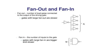
- 2. It is a basic concept of that deals with the speed of transistor. Two additional factors that influence the operational speed of a gate need to be considered and they are 1.FAN-IN 2.FAN-OUT Note:- 1.As fan-in have indicating that if no of inputs to gate increases then it increases the delay. 2.As fan-out have indicating no. of loads driven by the output the gate delay substantially increases.
- 6. Fan-in and Fan-out Characteristics
- 7. Choice of Layers:- • In order to meet a given specification of a designer will have several possible ways to choice the layers. • And any designer should have commonsense constraints to be considered. 1. VDD and Vss (GND) should be distributed on metal layers wherever possible. 2. Long lengths of polysilicon should be used only after careful consideration because of the relatively high RS value . Polysilicon is unsuitable for routing VDD or Vss other than for very small distances. 3. Diffusion layer will have moderate resistance