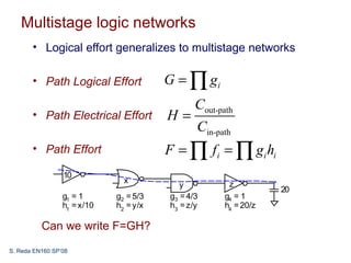
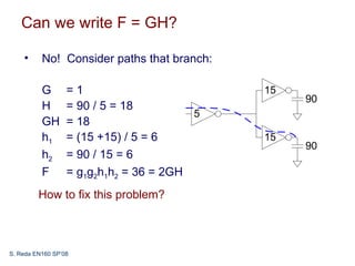
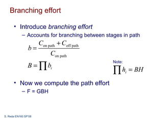
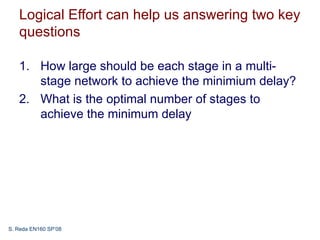
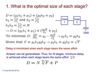
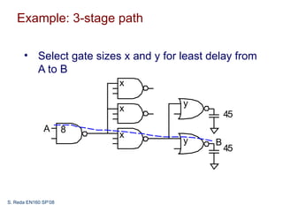
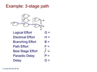
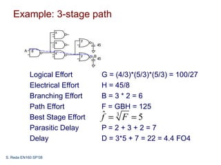
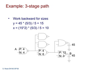
Design and Implementation of VLSI Systems
                   (EN1600)
                      Lecture 13: Logical Effort (2/2)


S. Reda EN160 SP’08
Multistage logic networks
       • Logical effort generalizes to multistage networks

       • Path Logical Effort            G = ∏ gi
                                               Cout-path
       • Path Electrical Effort         H=
                                               Cin-path
       • Path Effort                    F = ∏ f i = ∏ gi hi
                 10
                               x                       z
                                           y
                                                                  20
                 g1 = 1      g2 = 5/3   g3 = 4/3      g4 = 1
                 h1 = x/10   h2 = y/x   h3 = z/y      h4 = 20/z

          Can we write F=GH?
S. Reda EN160 SP’08
Can we write F = GH?

    •     No! Consider paths that branch:

          G       =1                        15
                                                 90
          H       = 90 / 5 = 18
                                        5
          GH      = 18
          h1      = (15 +15) / 5 = 6        15
                                                 90
          h2      = 90 / 15 = 6
          F       = g1g2h1h2 = 36 = 2GH
         How to fix this problem?


S. Reda EN160 SP’08
Branching effort

      • Introduce branching effort
            – Accounts for branching between stages in path
                      Con path + Coff path
                b=
                           Con path
                B = ∏ bi
                                                Note:

                                                ∏h      i   = BH
      • Now we compute the path effort
            – F = GBH


S. Reda EN160 SP’08
Logical Effort can help us answering two key
   questions

   1. How large should be each stage in a multi-
      stage network to achieve the minimium delay?
   2. What is the optimal number of stages to
      achieve the minimum delay


S. Reda EN160 SP’08
1. What is the optimal size of each stage?

                                              Gate      Gate
                                               1         2


                                                               GND


   Delay is minimized when each stage bears the same effort

    Answer can be generalized. Thus, for N stages, minimum delay
    is achieved when each stage bears the same effort


S. Reda EN160 SP’08
Example: 3-stage path

      • Select gate sizes x and y for least delay from
        A to B
                          x

                                      y
                          x
                                                 45
              A       8
                          x
                                      y      B
                                                 45


S. Reda EN160 SP’08
Example: 3-stage path
                      x

                            y
                      x
                                     45
         A   8
                      x
                            y    B
                                     45


             Logical Effort               G=
             Electrical Effort            H=
             Branching Effort             B=
             Path Effort                  F=
             Best Stage Effort            ˆ
                                          f =
             Parasitic Delay              P=
             Delay                        D=

S. Reda EN160 SP’08
Example: 3-stage path
                      x

                            y
                      x
                                     45
         A   8
                      x
                            y    B
                                     45


             Logical Effort               G = (4/3)*(5/3)*(5/3) = 100/27
             Electrical Effort            H = 45/8
             Branching Effort             B=3*2=6
             Path Effort                  F = GBH = 125
             Best Stage Effort            ˆ
                                          f = 3 F =5
             Parasitic Delay              P=2+3+2=7
             Delay                        D = 3*5 + 7 = 22 = 4.4 FO4

S. Reda EN160 SP’08
Example: 3-stage path

      •     Work backward for sizes
            y = 45 * (5/3) / 5 = 15
            x = (15*2) * (5/3) / 5 = 10


                                                      45
              A P: 4
                               P: 4
                N: 4                      P: 12   B
                               N: 6                   45
                                          N: 3


S. Reda EN160 SP’08
2. What is the optimal number of stages?

      • Consider adding inverters to end of path
            – How many give least delay?      Logic Block:
                                                              N - n1 ExtraInverters

                                               n1Stages
                           n1                 Path Effort F

          D = NF + ∑ pi + ( N − n1 ) pinv
                      1
                      N


                           i =1
          ∂D      1    1   1
             = − F ln F + F + pinv = 0
                  N    N   N

          ∂N
                                                 1
           Define best stage effort ρ = F        N


                  pinv + ρ ( 1 − ln ρ ) = 0


S. Reda EN160 SP’08
Optimal number of stages
    •      pinv + ρ ( 1 − ln ρ ) = 0 has no closed-form solution
    • Neglecting parasitics (pinv = 0), we find r = 2.718 (e)
    • For pinv = 1, solve numerically for r = 3.59
    • A path achieves least delay by using               stages
    • How sensitive is delay to using exactly the best number
      of stages?                               1.6
                                                     1.51


                                  D(N) /D(N)
    • ρ = 4 is reasonable                      1.4

                                               1.2                        1.15
                                                                                 1.26


                                               1.0

                                                                  (ρ=6)           (ρ =2.4)


                                               0.0
                                                            0.5   0.7     1.0      1.4       2.0

                                                                          N/ N

S. Reda EN160 SP’08

Lecture13

  • 1.
    Design and Implementationof VLSI Systems (EN1600) Lecture 13: Logical Effort (2/2) S. Reda EN160 SP’08
  • 2.
    Multistage logic networks • Logical effort generalizes to multistage networks • Path Logical Effort G = ∏ gi Cout-path • Path Electrical Effort H= Cin-path • Path Effort F = ∏ f i = ∏ gi hi 10 x z y 20 g1 = 1 g2 = 5/3 g3 = 4/3 g4 = 1 h1 = x/10 h2 = y/x h3 = z/y h4 = 20/z Can we write F=GH? S. Reda EN160 SP’08
  • 3.
    Can we writeF = GH? • No! Consider paths that branch: G =1 15 90 H = 90 / 5 = 18 5 GH = 18 h1 = (15 +15) / 5 = 6 15 90 h2 = 90 / 15 = 6 F = g1g2h1h2 = 36 = 2GH How to fix this problem? S. Reda EN160 SP’08
  • 4.
    Branching effort • Introduce branching effort – Accounts for branching between stages in path Con path + Coff path b= Con path B = ∏ bi Note: ∏h i = BH • Now we compute the path effort – F = GBH S. Reda EN160 SP’08
  • 5.
    Logical Effort canhelp us answering two key questions 1. How large should be each stage in a multi- stage network to achieve the minimium delay? 2. What is the optimal number of stages to achieve the minimum delay S. Reda EN160 SP’08
  • 6.
    1. What isthe optimal size of each stage? Gate Gate 1 2 GND Delay is minimized when each stage bears the same effort Answer can be generalized. Thus, for N stages, minimum delay is achieved when each stage bears the same effort S. Reda EN160 SP’08
  • 7.
    Example: 3-stage path • Select gate sizes x and y for least delay from A to B x y x 45 A 8 x y B 45 S. Reda EN160 SP’08
  • 8.
    Example: 3-stage path x y x 45 A 8 x y B 45 Logical Effort G= Electrical Effort H= Branching Effort B= Path Effort F= Best Stage Effort ˆ f = Parasitic Delay P= Delay D= S. Reda EN160 SP’08
  • 9.
    Example: 3-stage path x y x 45 A 8 x y B 45 Logical Effort G = (4/3)*(5/3)*(5/3) = 100/27 Electrical Effort H = 45/8 Branching Effort B=3*2=6 Path Effort F = GBH = 125 Best Stage Effort ˆ f = 3 F =5 Parasitic Delay P=2+3+2=7 Delay D = 3*5 + 7 = 22 = 4.4 FO4 S. Reda EN160 SP’08
  • 10.
    Example: 3-stage path • Work backward for sizes y = 45 * (5/3) / 5 = 15 x = (15*2) * (5/3) / 5 = 10 45 A P: 4 P: 4 N: 4 P: 12 B N: 6 45 N: 3 S. Reda EN160 SP’08
  • 11.
    2. What isthe optimal number of stages? • Consider adding inverters to end of path – How many give least delay? Logic Block: N - n1 ExtraInverters n1Stages n1 Path Effort F D = NF + ∑ pi + ( N − n1 ) pinv 1 N i =1 ∂D 1 1 1 = − F ln F + F + pinv = 0 N N N ∂N 1 Define best stage effort ρ = F N pinv + ρ ( 1 − ln ρ ) = 0 S. Reda EN160 SP’08
  • 12.
    Optimal number ofstages • pinv + ρ ( 1 − ln ρ ) = 0 has no closed-form solution • Neglecting parasitics (pinv = 0), we find r = 2.718 (e) • For pinv = 1, solve numerically for r = 3.59 • A path achieves least delay by using stages • How sensitive is delay to using exactly the best number of stages? 1.6 1.51 D(N) /D(N) • ρ = 4 is reasonable 1.4 1.2 1.15 1.26 1.0 (ρ=6) (ρ =2.4) 0.0 0.5 0.7 1.0 1.4 2.0 N/ N S. Reda EN160 SP’08