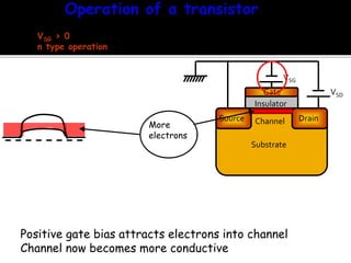
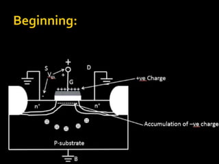
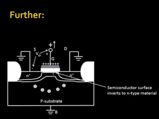
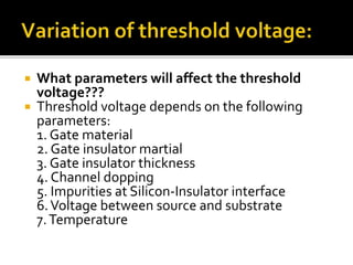
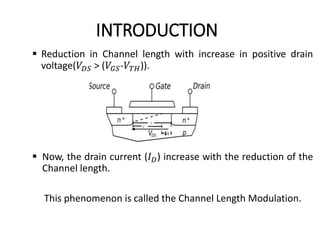
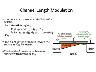
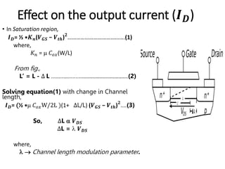
Threshold Voltage
&
Channel Length Modulation
1.ThresholdVoltage Introduction
1. 1st Stage
2. 2nd Stage
2. Factors for variation inThesholdVoltage
3.SubthresholdVoltage
4. Channel Length Modulation
a) Introduction
b) Effect on output current.
Substrate
Channel Drain
Insulator
Gate
VSG > 0
n type operation
Positive gate bias attracts electrons into channel
Channel now becomes more conductive
More
electrons
Source
VSD
VSG
 What parameters will affect the threshold
voltage???
 Threshold voltage depends on the following
parameters:
1. Gate material
2. Gate insulator martial
3. Gate insulator thickness
4. Channel dopping
5. Impurities at Silicon-Insulator interface
6.Voltage between source and substrate
7.Temperature
CHANNEL LENGTH MODULATION
INTRODUCTION
 Reduction in Channel length with increase in positive drain
voltage(𝑉𝐷𝑆 > (𝑉𝐺𝑆-𝑉𝑇𝐻)).
 Now, the drain current (𝐼 𝐷) increase with the reduction of the
Channel length.
This phenomenon is called the Channel Length Modulation.
Channel Length Modulation
 It occurs when transistor is in Saturation
region.
i.e. Saturation region,
𝑉𝐺𝑆>𝑉𝑡ℎ and 𝑉𝐷𝑆> 𝑉𝐺𝑆 - 𝑉𝑡ℎ
𝐼 𝐷 increases slightly with increasing
𝑉𝐷𝑆 .
 The pinch-off point moves toward the
source as 𝑉𝐷𝑆 increases.
 The length of the channel becomes
shorter with increasing 𝑉𝐷𝑆.
Effect on the output current (𝑰 𝑫)
• In Saturation region,
𝑰 𝑫= ½ ∗𝑲 𝒏(𝑽 𝑮𝑺 − 𝑽 𝒕𝒉) 𝟐
………………………………….(1)
where,
𝐾 𝑛 =  𝐶 𝑜𝑥(W/L)
From fig.,
L’ = L - ∆ L ………………….................................(2)
Solving equation(1) with change in Channel
length,
𝑰 𝑫= (½ ∗ 𝐶 𝑜𝑥W/2L )(1+ ∆L/L) (𝑽 𝑮𝑺 − 𝑽 𝒕𝒉) 𝟐
….(3)
So, ∆L  𝑽 𝑫𝑺
∆L =  𝑽 𝑫𝑺
where,
  Channel length modulation parameter.
Contd………
Therefore,
𝑰 𝑫= ½ ∗𝑲 𝒏(𝑽 𝑮𝑺 − 𝑽 𝒕𝒉) 𝟐
(1 +𝑽 𝑫𝑺)............(4)
 The early voltage,
-𝑽 𝑨 = - 1/ 
 Output resistance between source
and drain is given by,
𝒓 𝒐= 1/(𝑰 𝑫) = 𝑽 𝑨/𝑰 𝑫
REFERENCES:
[1] http://www.onmyphd.com/print.php?p=channel.length.modulation
[2] Modern VLSI Design-by Yuan Taur and Tak H. Ning
[3] https://ecee.colorado.edu/~bart/book/book/chapter7/ch7_3
[4] https://www.researchgate.net/post/
[5] http://nptel.ac.in/courses/117103063/17
Threshold Voltage & Channel Length Modulation

Threshold Voltage & Channel Length Modulation

  • 1.
  • 2.
    1.ThresholdVoltage Introduction 1. 1stStage 2. 2nd Stage 2. Factors for variation inThesholdVoltage 3.SubthresholdVoltage 4. Channel Length Modulation a) Introduction b) Effect on output current.
  • 3.
    Substrate Channel Drain Insulator Gate VSG >0 n type operation Positive gate bias attracts electrons into channel Channel now becomes more conductive More electrons Source VSD VSG
  • 7.
     What parameterswill affect the threshold voltage???  Threshold voltage depends on the following parameters: 1. Gate material 2. Gate insulator martial 3. Gate insulator thickness 4. Channel dopping 5. Impurities at Silicon-Insulator interface 6.Voltage between source and substrate 7.Temperature
  • 9.
  • 10.
    INTRODUCTION  Reduction inChannel length with increase in positive drain voltage(𝑉𝐷𝑆 > (𝑉𝐺𝑆-𝑉𝑇𝐻)).  Now, the drain current (𝐼 𝐷) increase with the reduction of the Channel length. This phenomenon is called the Channel Length Modulation.
  • 11.
    Channel Length Modulation It occurs when transistor is in Saturation region. i.e. Saturation region, 𝑉𝐺𝑆>𝑉𝑡ℎ and 𝑉𝐷𝑆> 𝑉𝐺𝑆 - 𝑉𝑡ℎ 𝐼 𝐷 increases slightly with increasing 𝑉𝐷𝑆 .  The pinch-off point moves toward the source as 𝑉𝐷𝑆 increases.  The length of the channel becomes shorter with increasing 𝑉𝐷𝑆.
  • 12.
    Effect on theoutput current (𝑰 𝑫) • In Saturation region, 𝑰 𝑫= ½ ∗𝑲 𝒏(𝑽 𝑮𝑺 − 𝑽 𝒕𝒉) 𝟐 ………………………………….(1) where, 𝐾 𝑛 =  𝐶 𝑜𝑥(W/L) From fig., L’ = L - ∆ L ………………….................................(2) Solving equation(1) with change in Channel length, 𝑰 𝑫= (½ ∗ 𝐶 𝑜𝑥W/2L )(1+ ∆L/L) (𝑽 𝑮𝑺 − 𝑽 𝒕𝒉) 𝟐 ….(3) So, ∆L  𝑽 𝑫𝑺 ∆L =  𝑽 𝑫𝑺 where,   Channel length modulation parameter.
  • 13.
    Contd……… Therefore, 𝑰 𝑫= ½∗𝑲 𝒏(𝑽 𝑮𝑺 − 𝑽 𝒕𝒉) 𝟐 (1 +𝑽 𝑫𝑺)............(4)  The early voltage, -𝑽 𝑨 = - 1/   Output resistance between source and drain is given by, 𝒓 𝒐= 1/(𝑰 𝑫) = 𝑽 𝑨/𝑰 𝑫
  • 14.
    REFERENCES: [1] http://www.onmyphd.com/print.php?p=channel.length.modulation [2] ModernVLSI Design-by Yuan Taur and Tak H. Ning [3] https://ecee.colorado.edu/~bart/book/book/chapter7/ch7_3 [4] https://www.researchgate.net/post/ [5] http://nptel.ac.in/courses/117103063/17