Downloaded 376 times
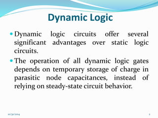
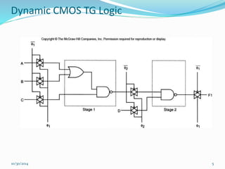
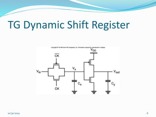
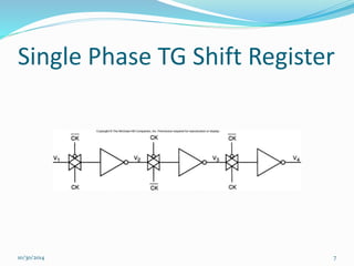
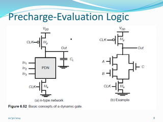
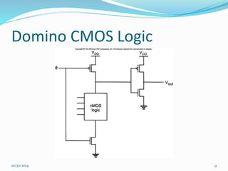
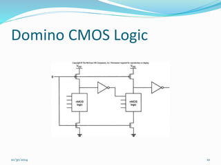
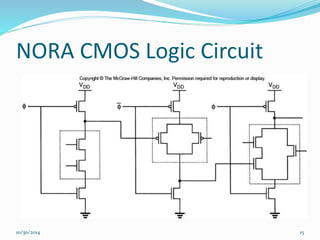
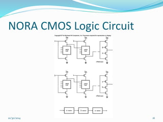
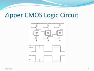
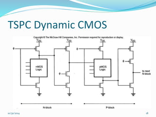
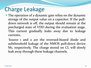
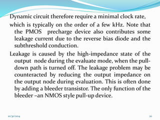
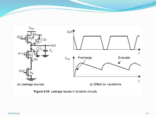
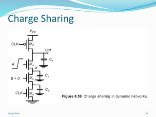
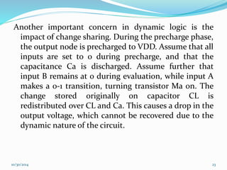


This document discusses dynamic logic circuits. It notes that dynamic logic circuits offer advantages over static logic circuits by temporarily storing charge in parasitic capacitances rather than relying on steady-state behavior. Dynamic logic circuits require periodic clock signals to control charge refreshing and allow for simple sequential circuits with memory. They can implement logic in smaller areas and thus consume less power than static logic. The document then discusses several examples of dynamic logic circuits like dynamic CMOS TG logic, domino CMOS logic, NORA logic, and their operating principles. It also covers issues like charge leakage and charge sharing that need to be addressed in dynamic logic circuits.