Download to read offline
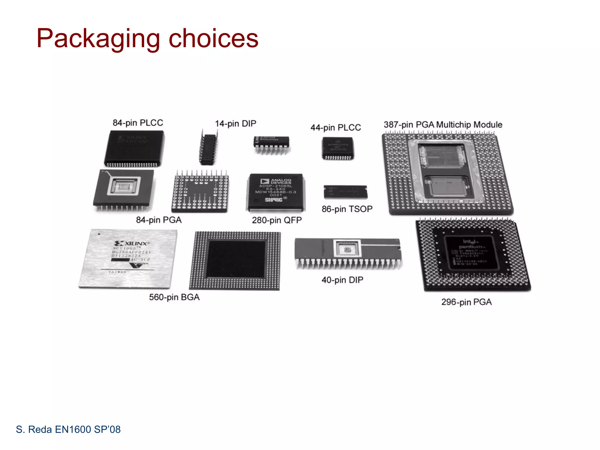
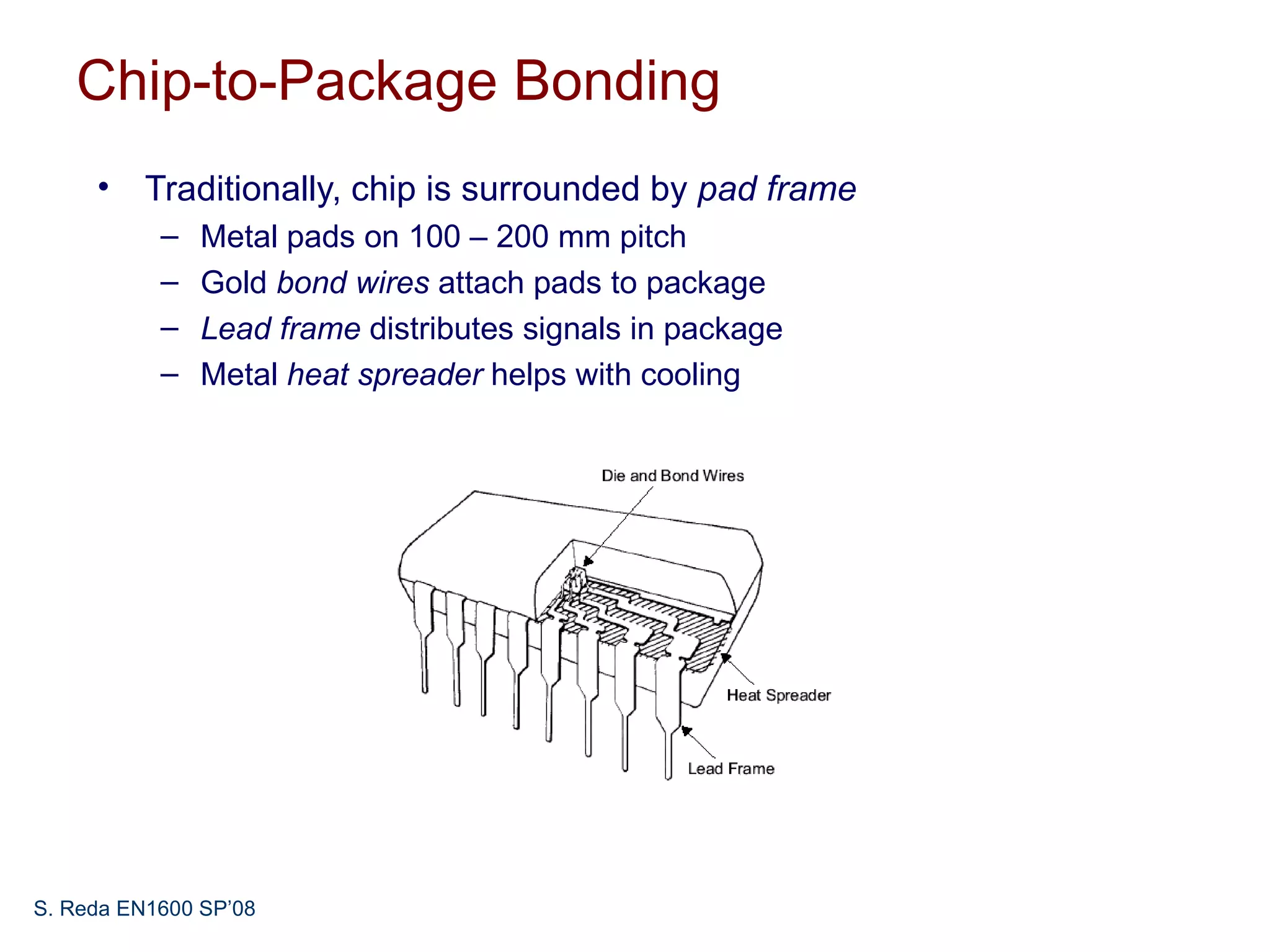
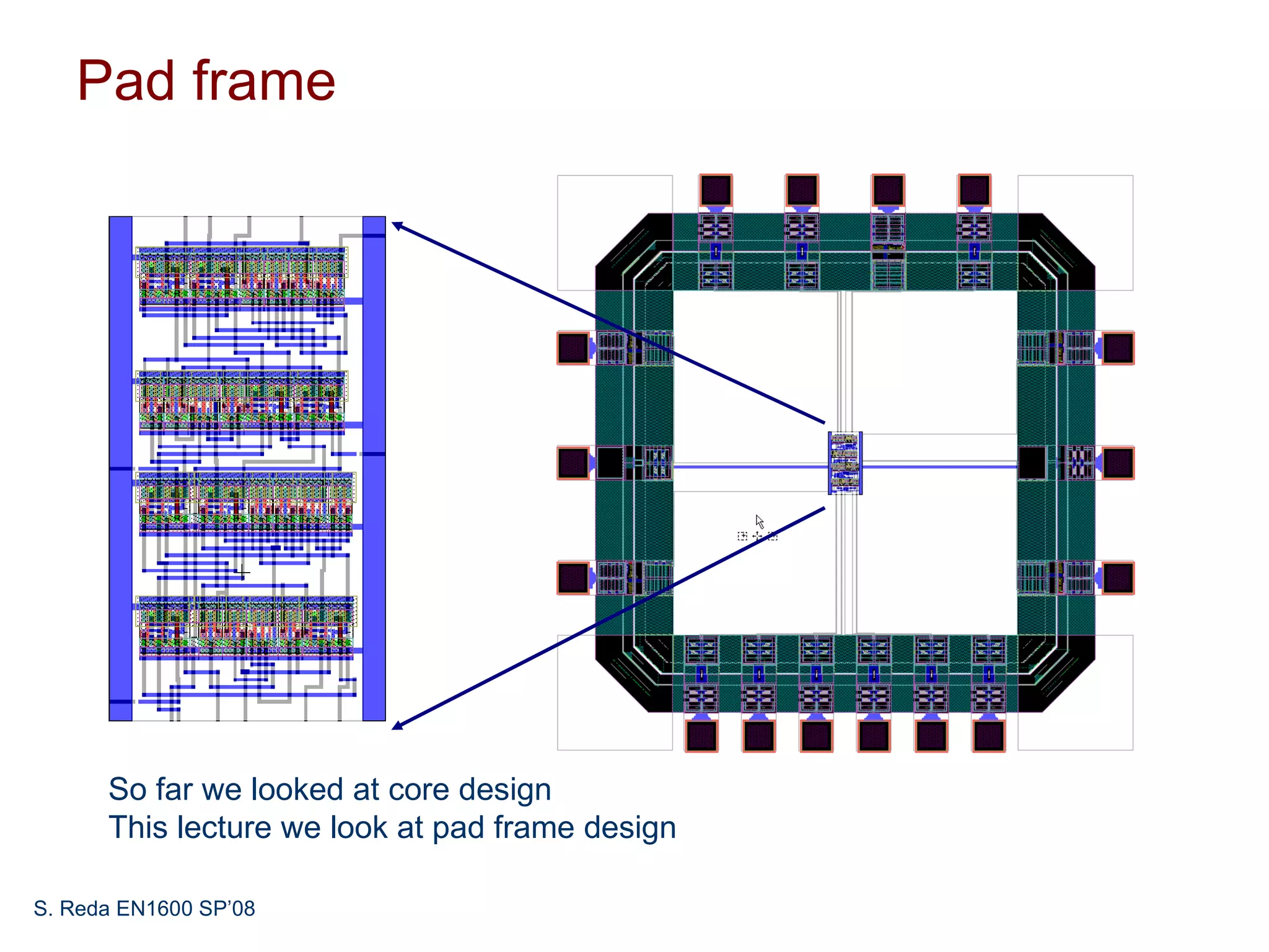
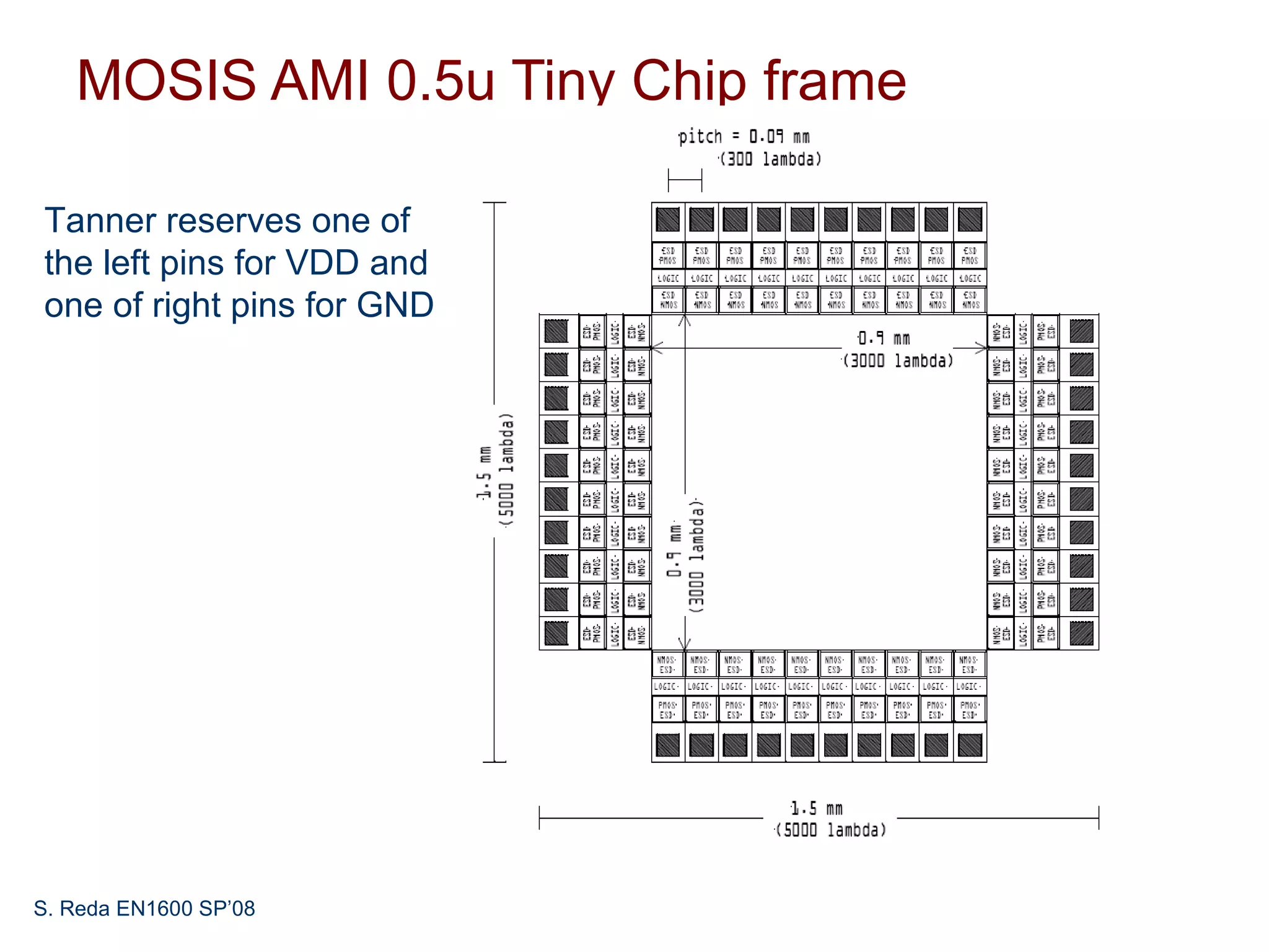
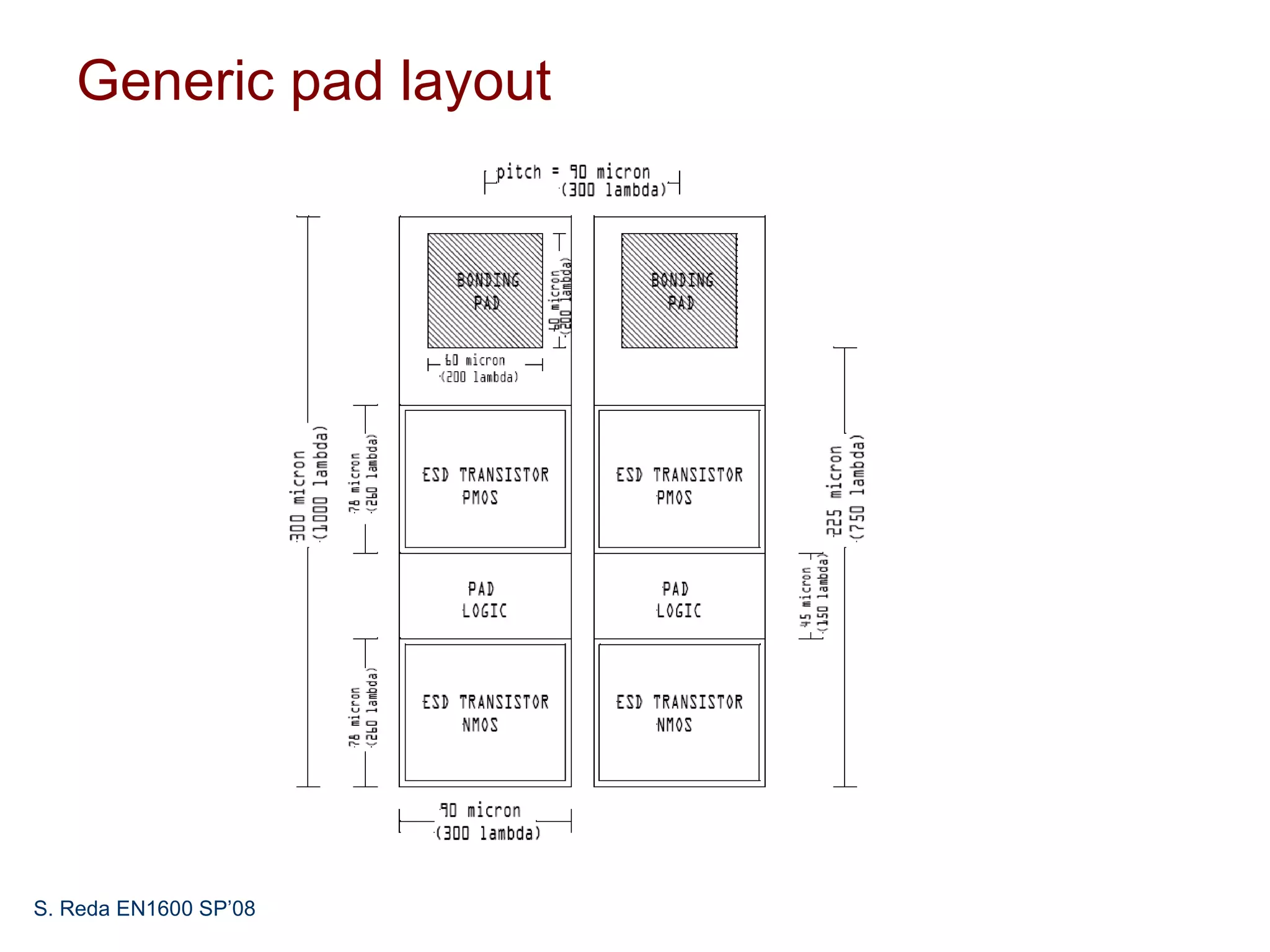
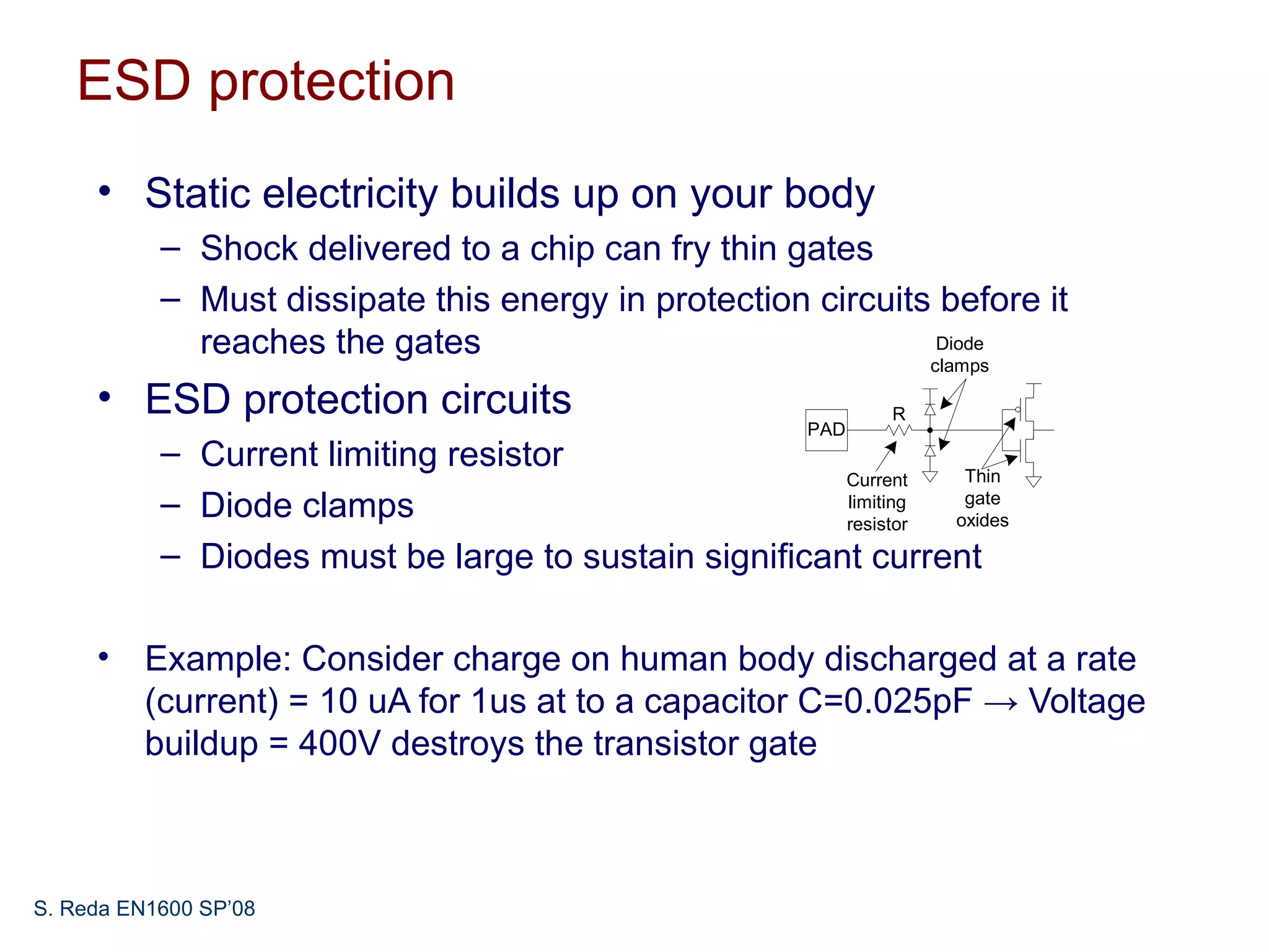
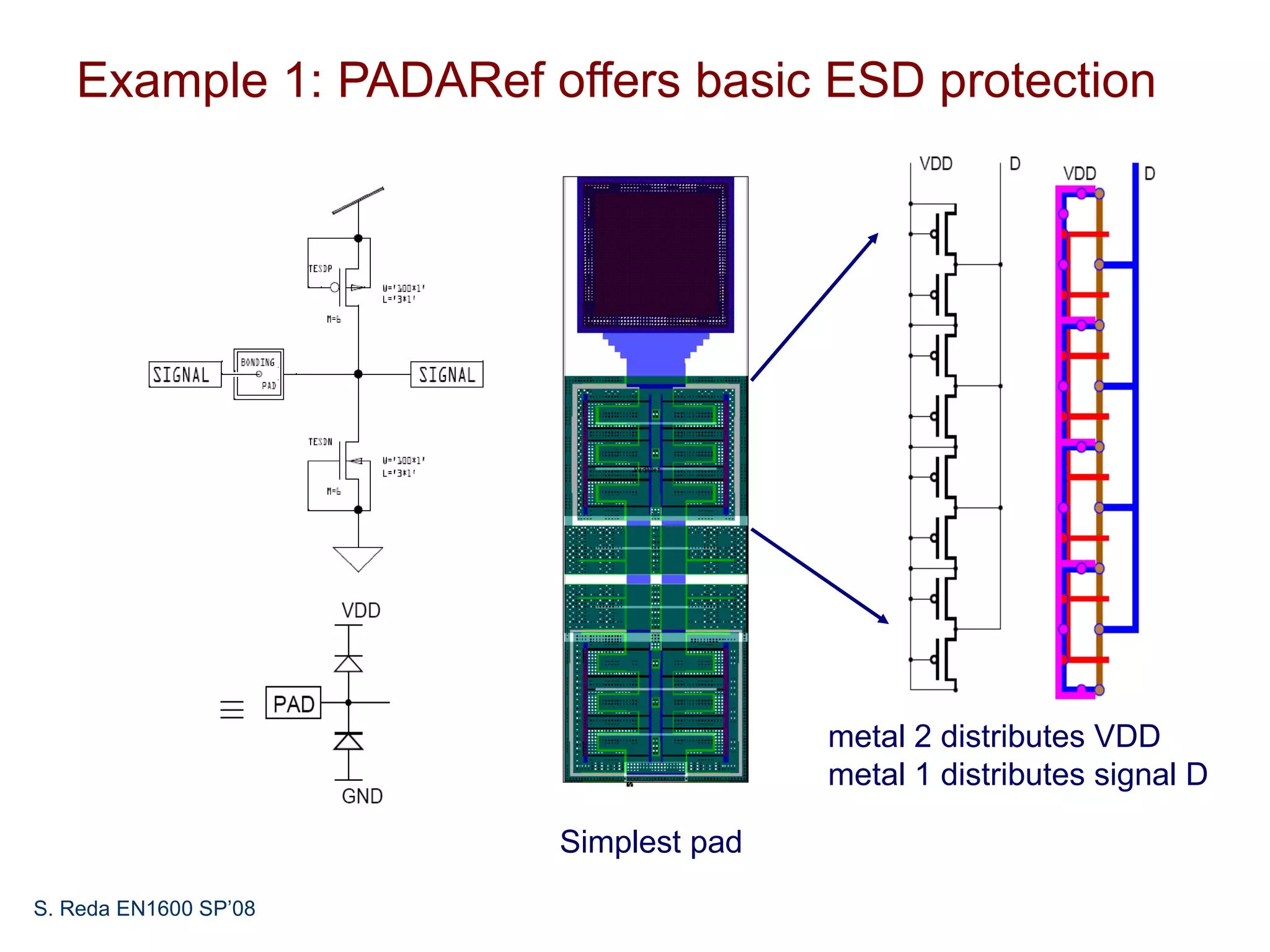
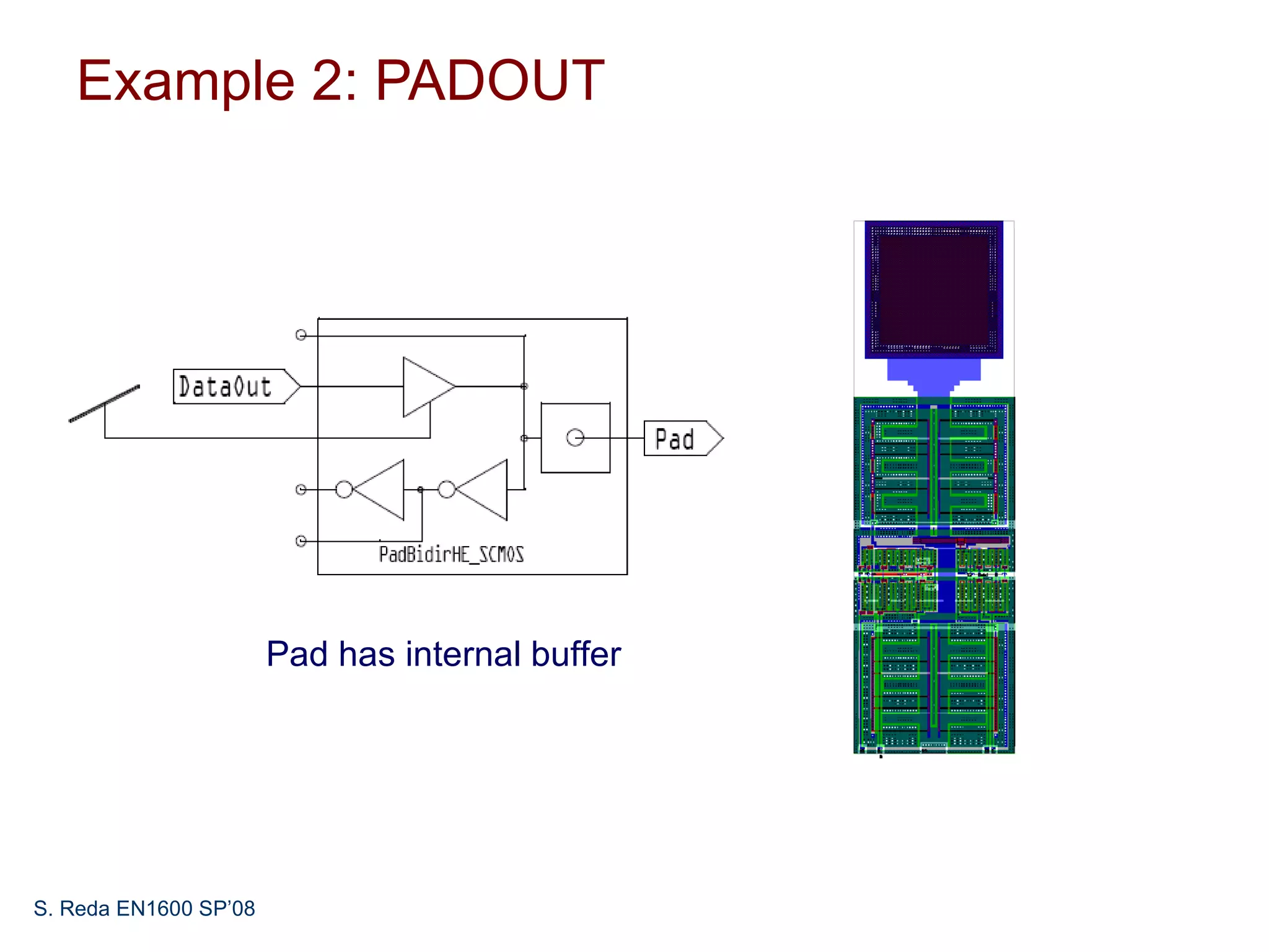
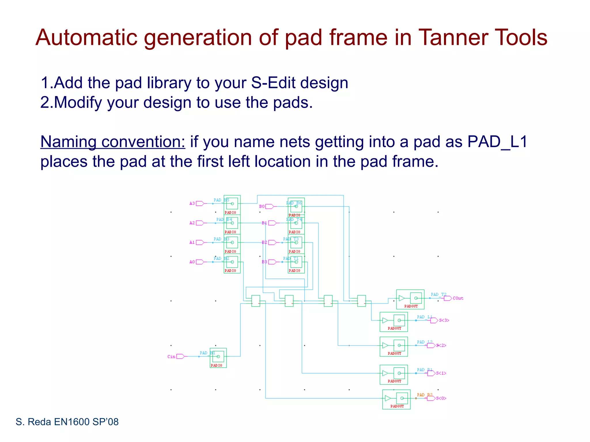
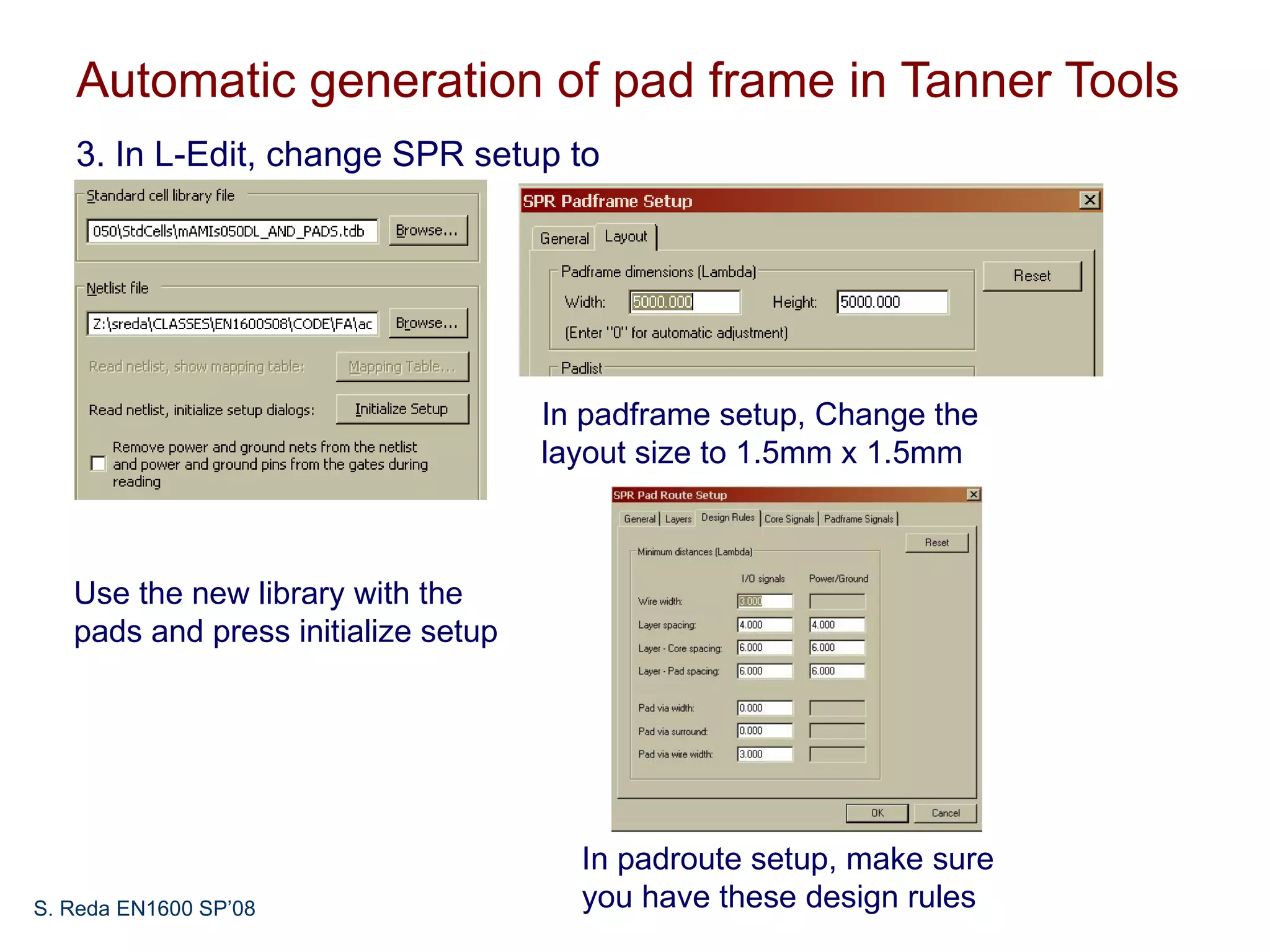
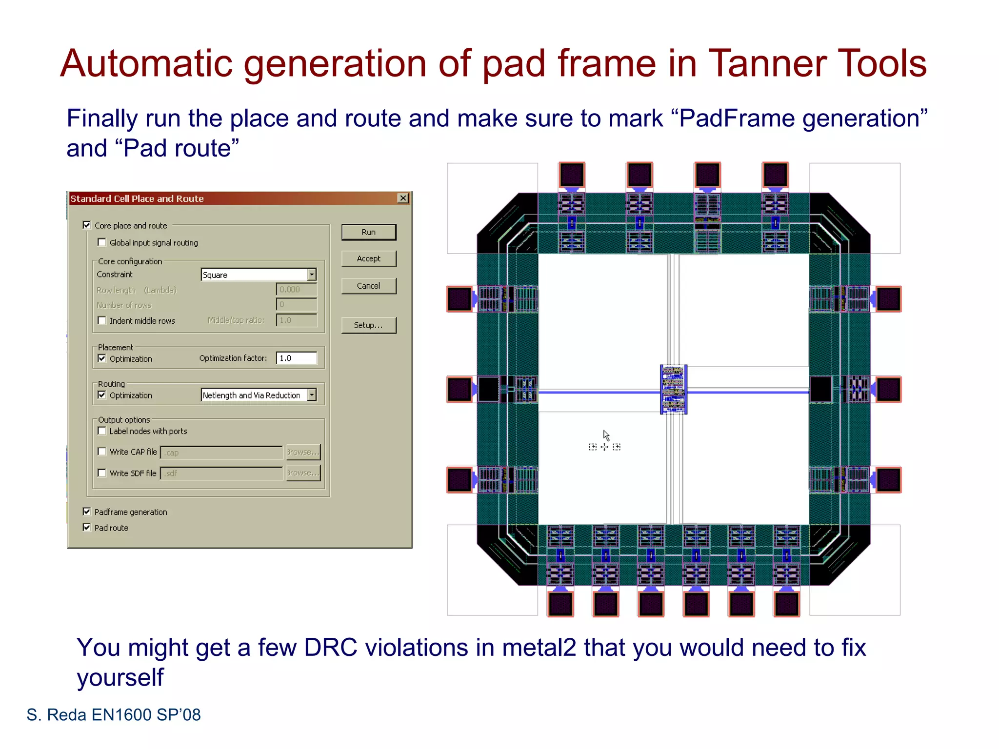

This document discusses pad frame design and packaging for VLSI systems. It covers chip-to-package bonding using gold bond wires to connect pads on the chip to the package. The pad frame distributes signals to the package and helps with cooling. The document provides an example of a MOSIS pad frame layout and discusses generic pad layout considerations. It also covers ESD protection circuits needed on pads to protect from static discharge and provides two examples of pad designs with ESD protection. Finally, it discusses automatically generating a pad frame in Tanner Tools by adding a pad library, modifying the design to use pads, and running the place and route while selecting options to generate the pad frame and route pads.