Downloaded 1,158 times

Diode-Transistor Logic (DTL) was an early logic family that used diodes and bipolar transistors. It suffered from voltage degradation between stages. Transistor-Transistor Logic (TTL) replaced the diode inputs of DTL with a single multi-emitter bipolar transistor, making it more area efficient. TTL also had faster switching speeds than DTL due to its use of an active pull-up transistor and totem-pole output. Standard TTL gates like the 7400 series had propagation delays of 12ns, fanout of 10, and power dissipation of 10mW.
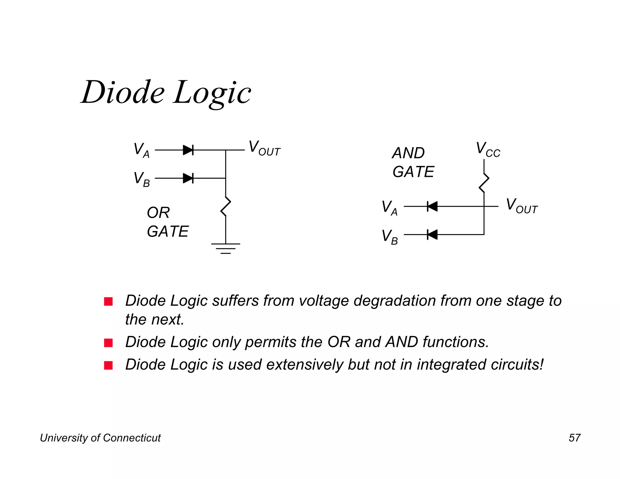
Introduction to DTL, discussing diode logic functions (AND, OR), voltage degradation, and limitations in integrated circuits.
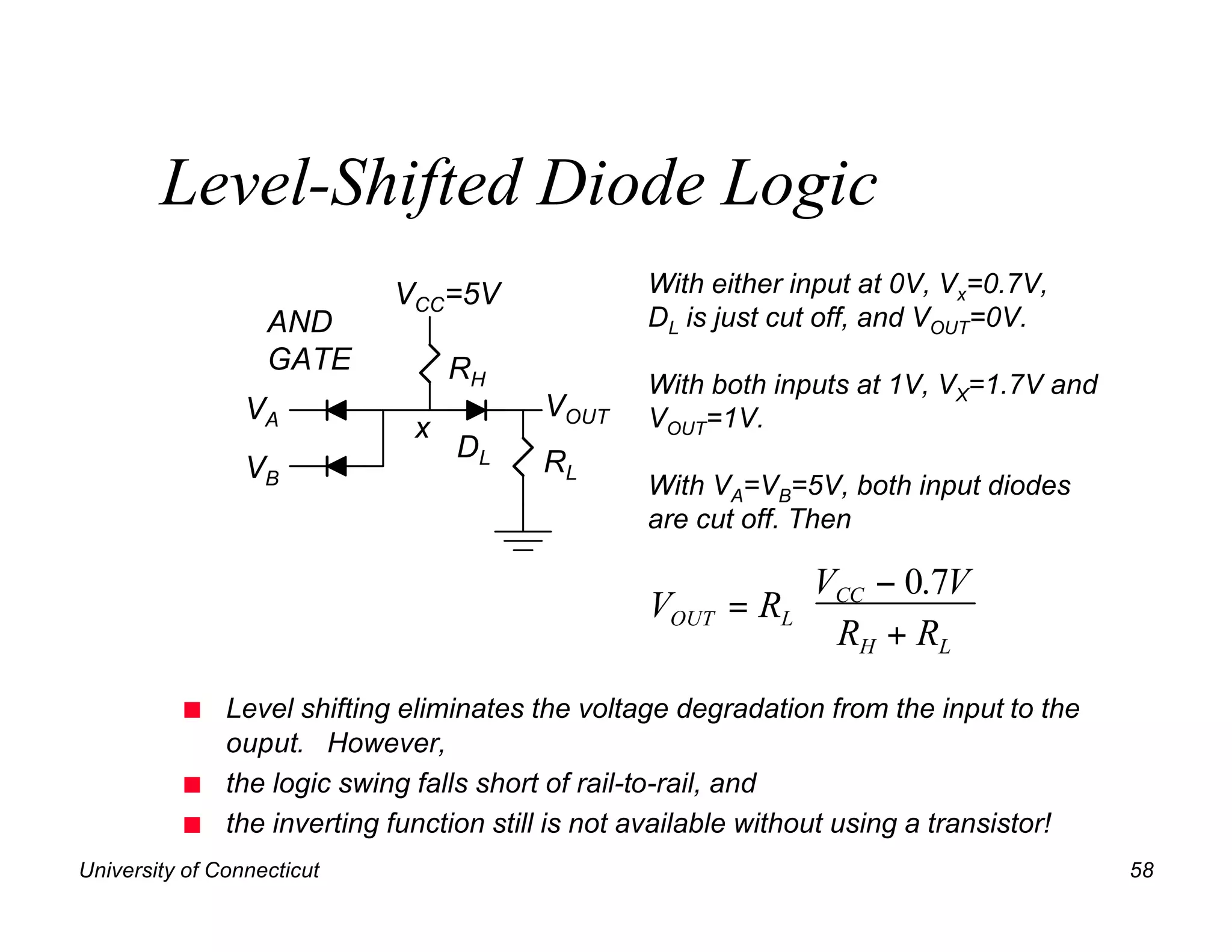
Explains level-shifted diode logic which avoids voltage degradation, and limitations like rail-to-rail logic and needing transistors for inversion.
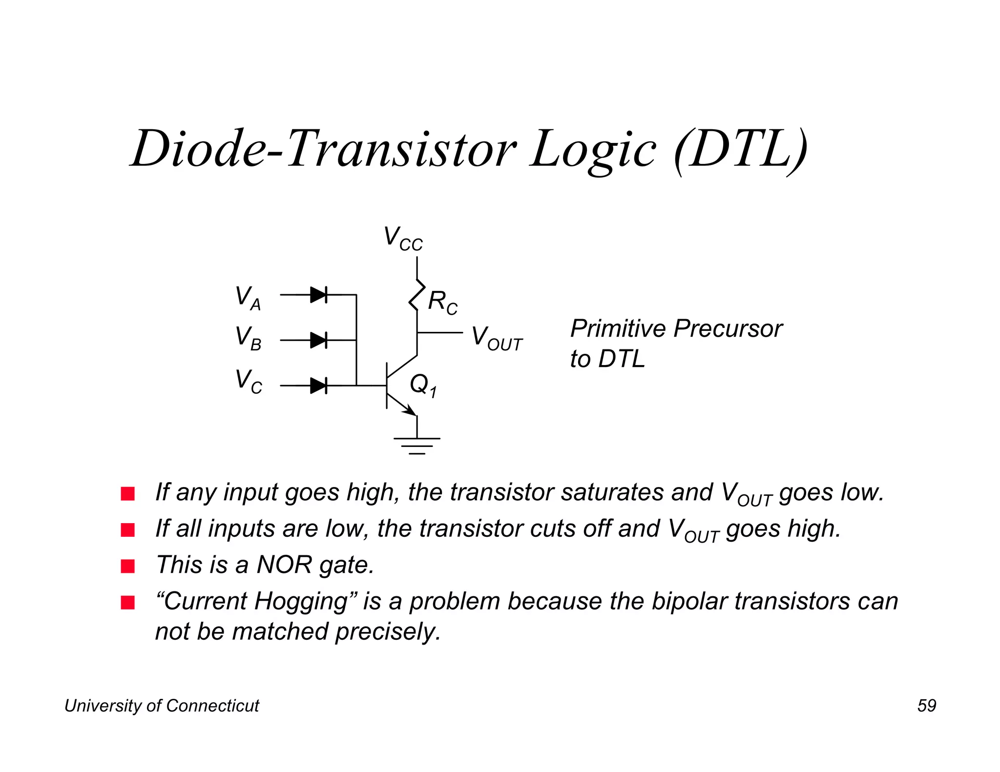
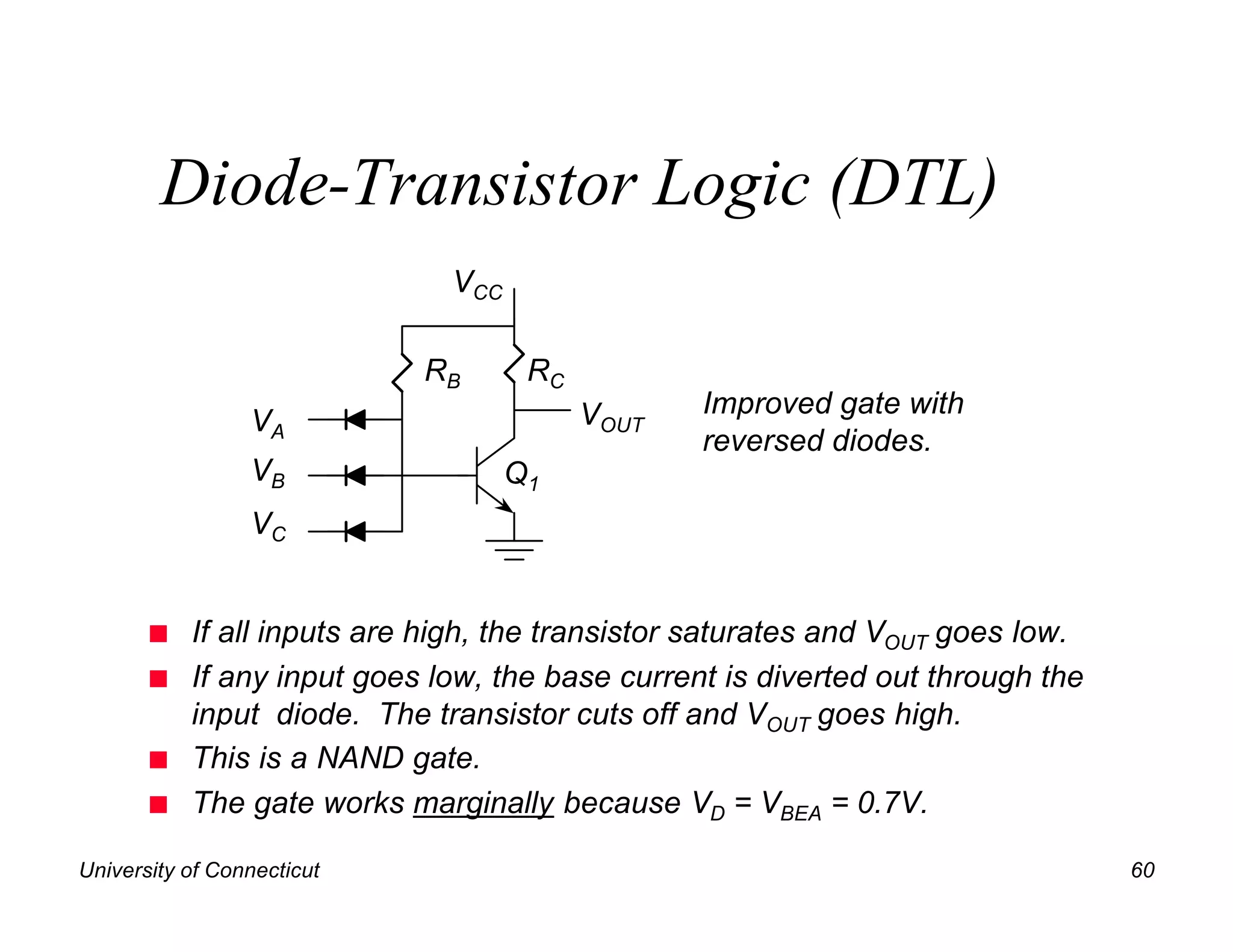
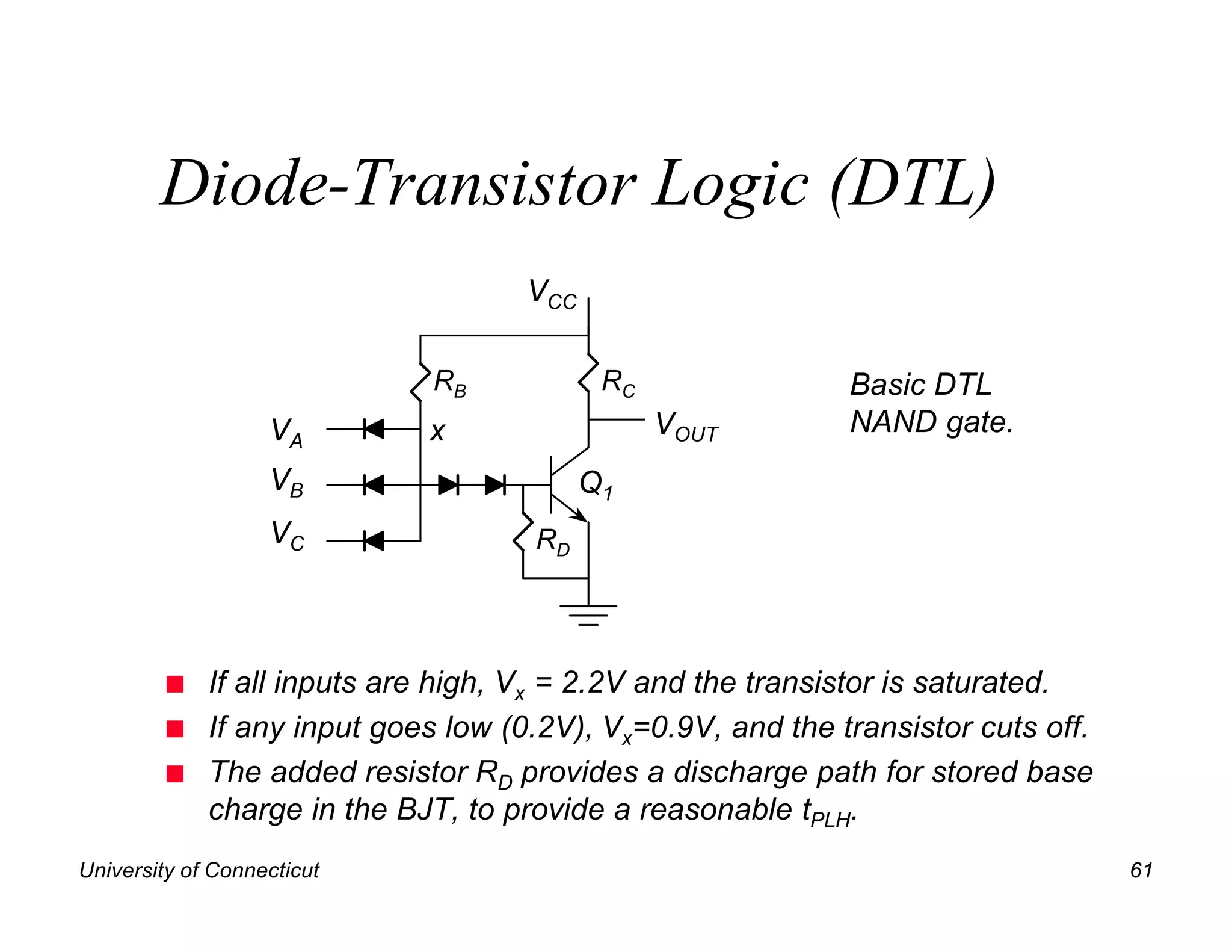
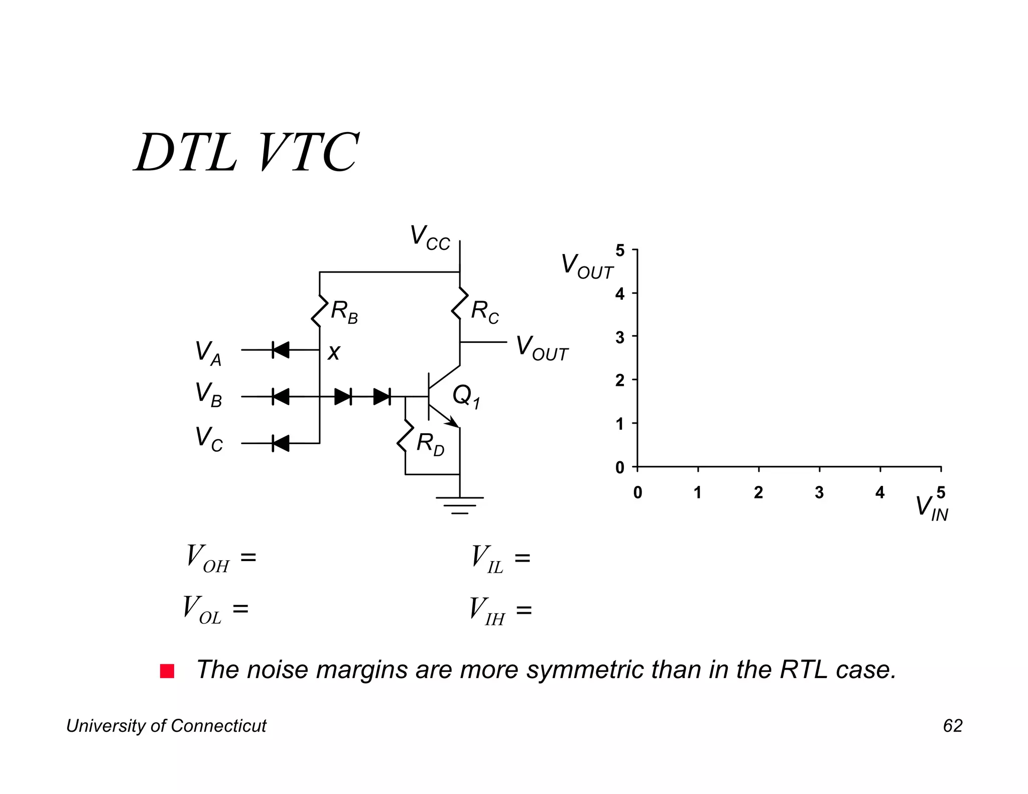
DTL structure, NOR and NAND gate operations, with emphasis on voltage outputs and current hogging challenges.
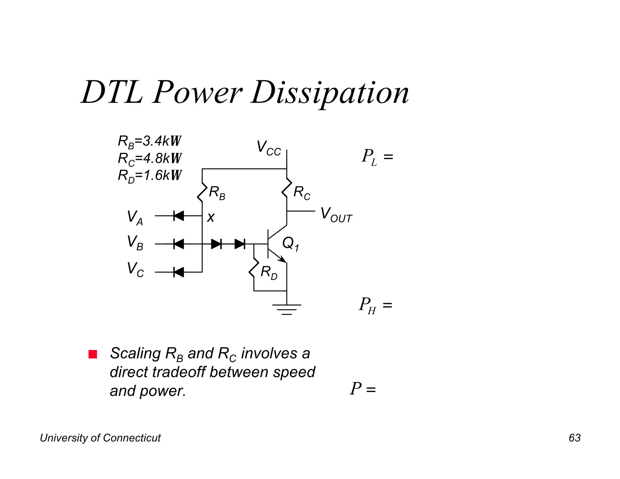
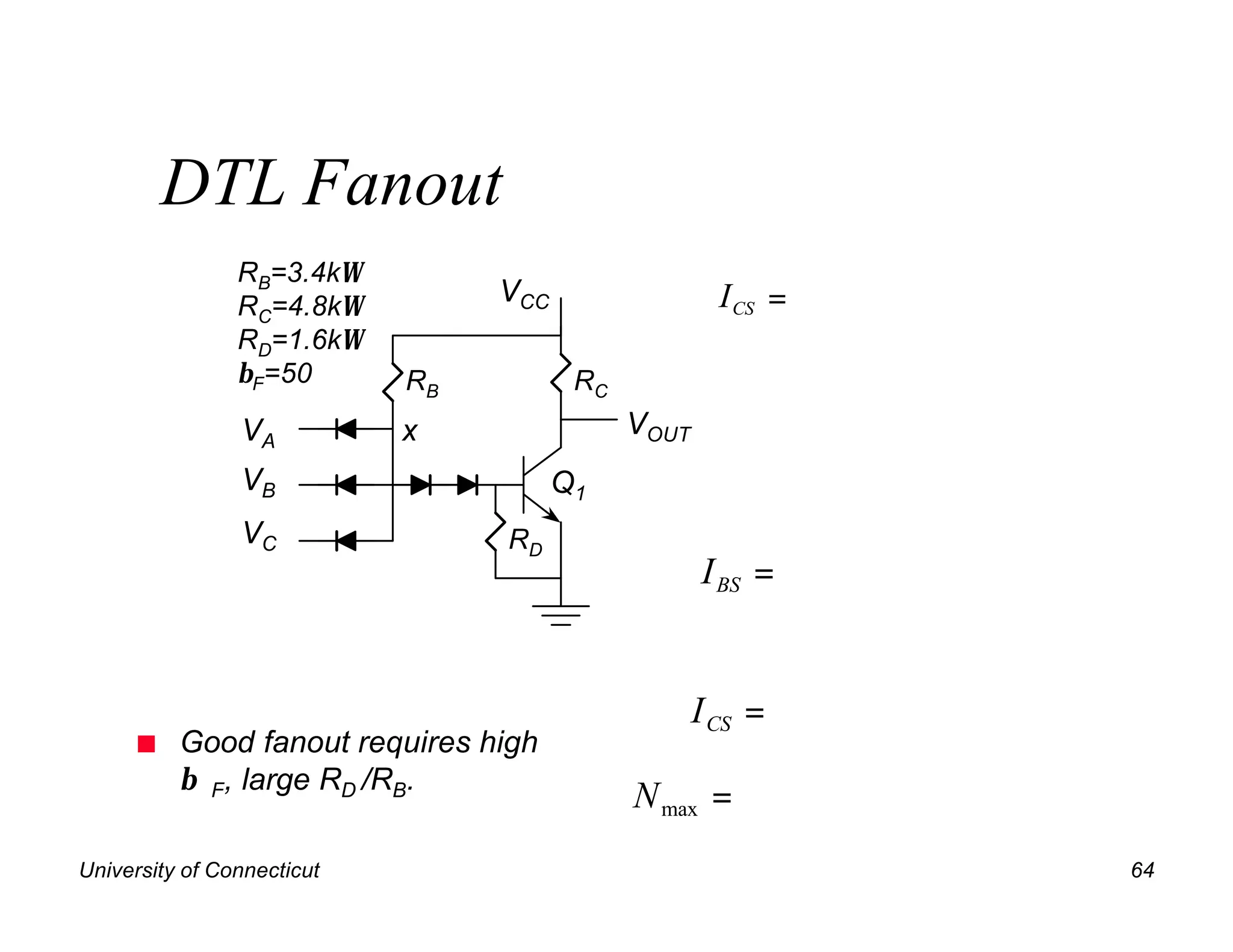
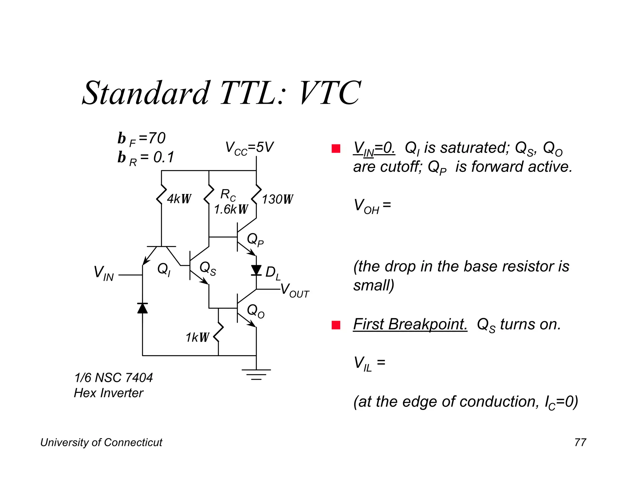
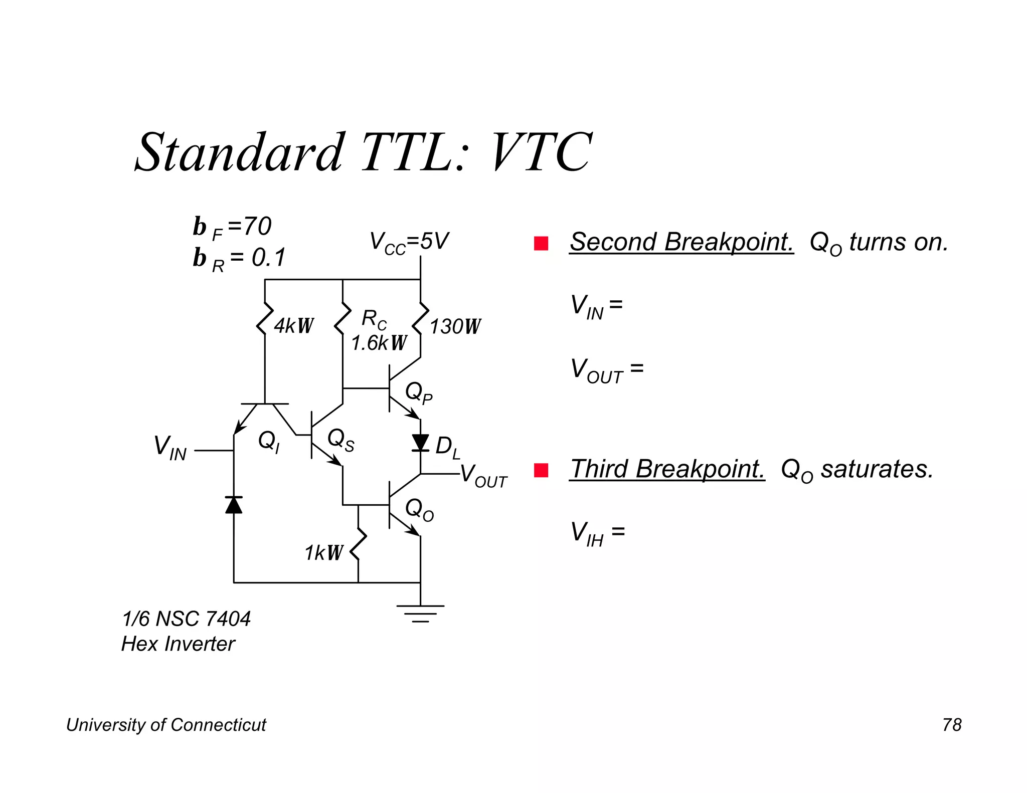
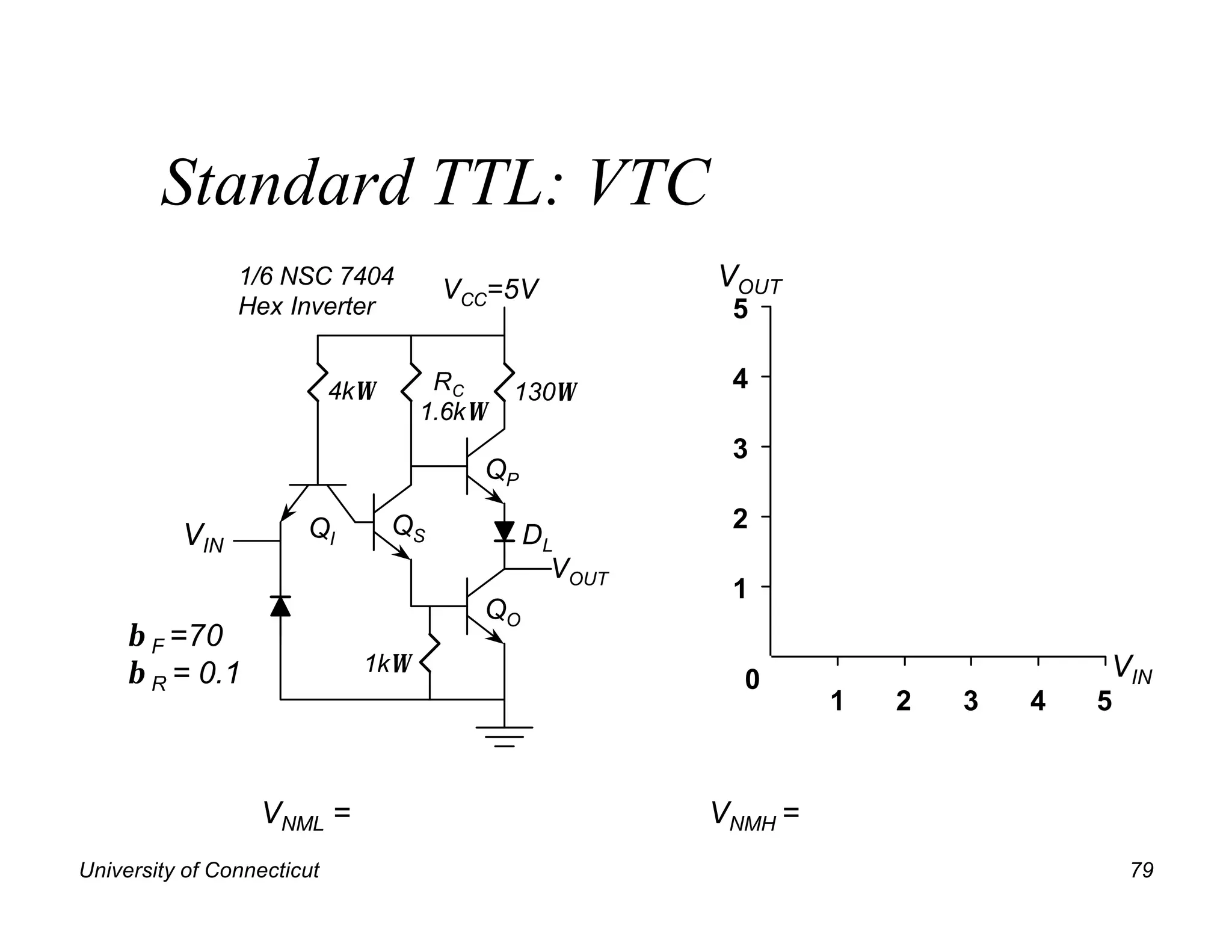
Voltage transfer characteristics (VTC), power dissipation considerations, fanout capabilities, and tradeoffs between speed and power.
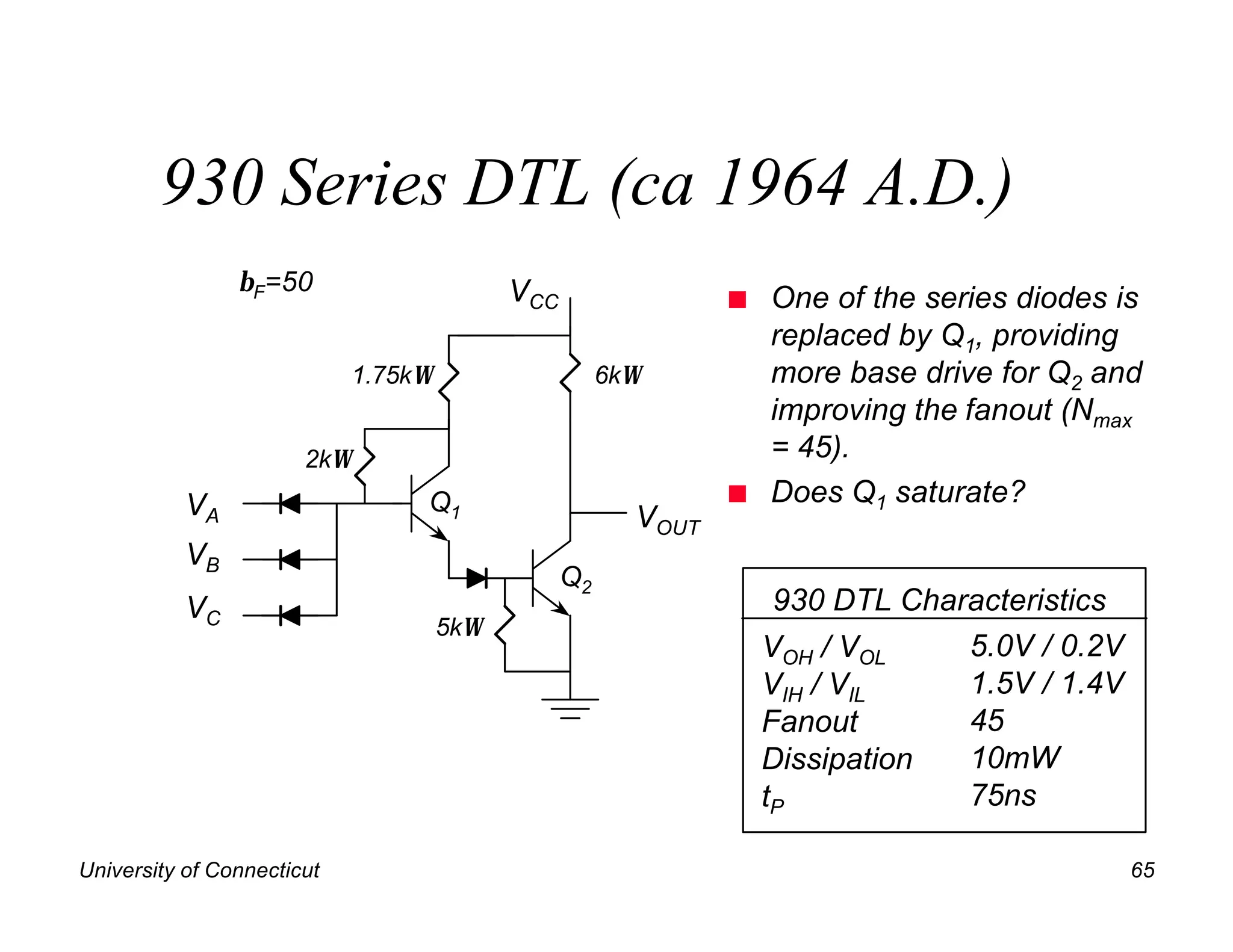
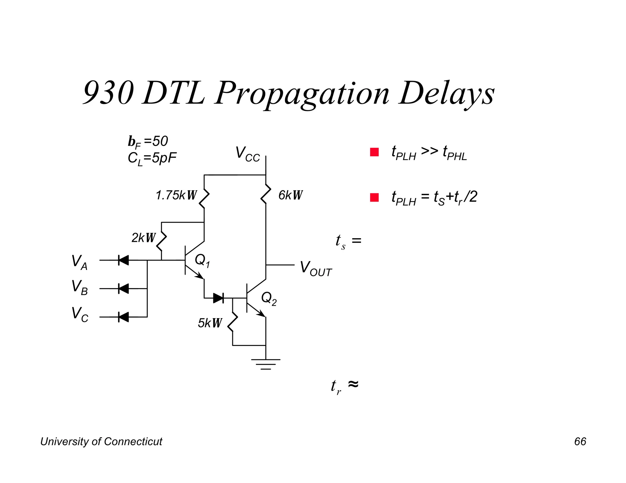
Introduction to the 930 series DTL, evolution from DTL to TTL, and specific characteristics like voltage outputs and propagation delays.
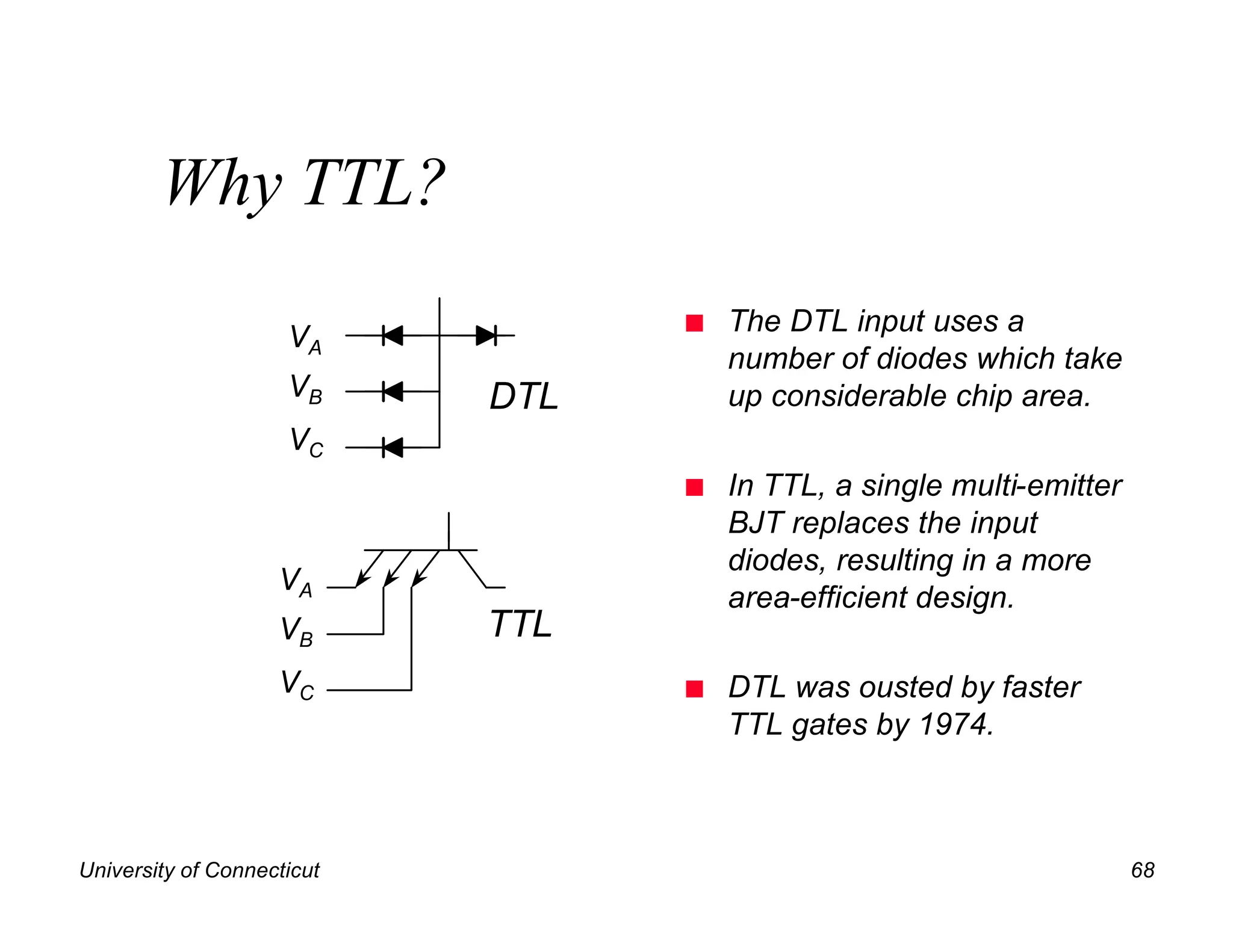
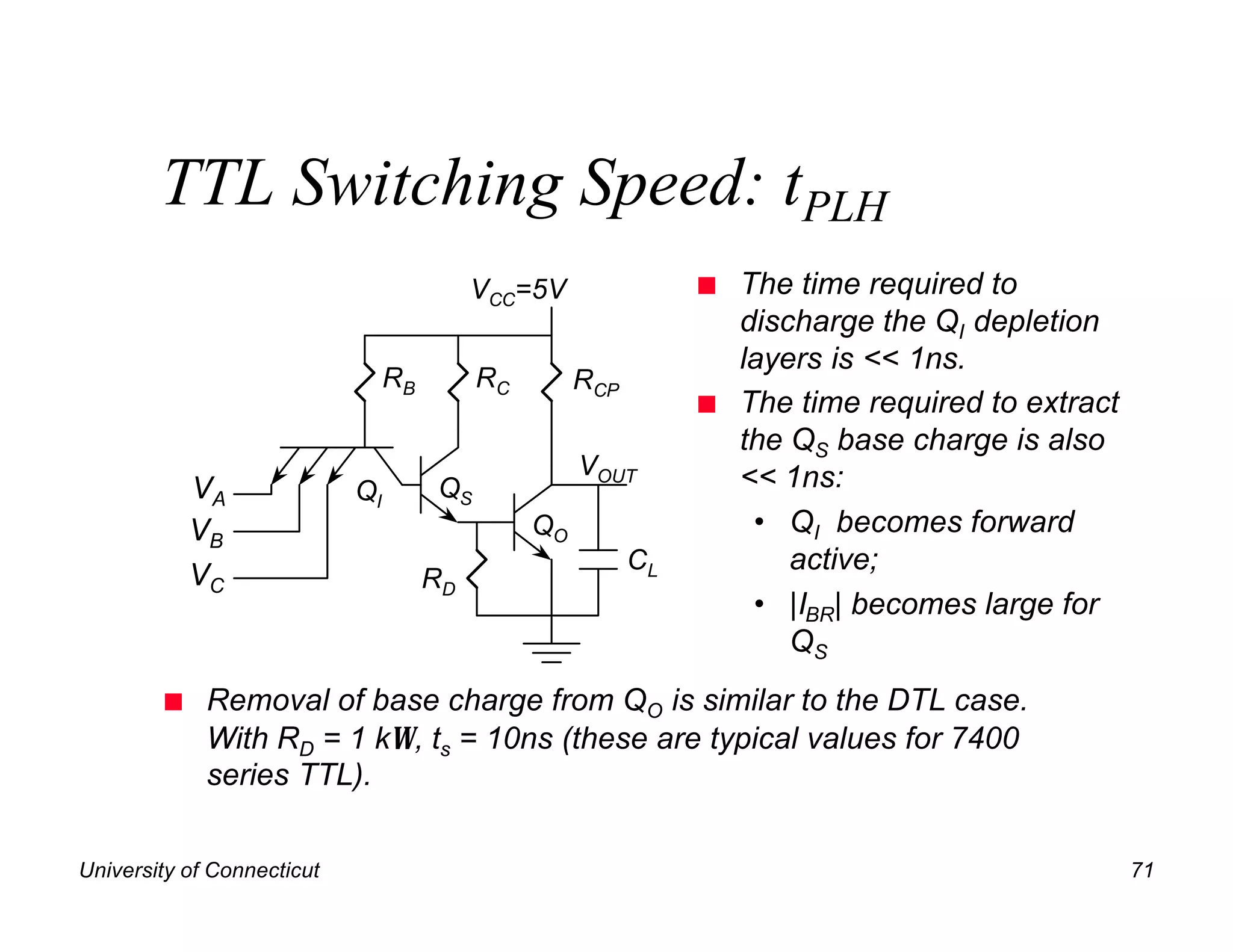
Comparison with DTL, highlighting design efficiency due to multi-emitter BJTs and improvements in switching speed.
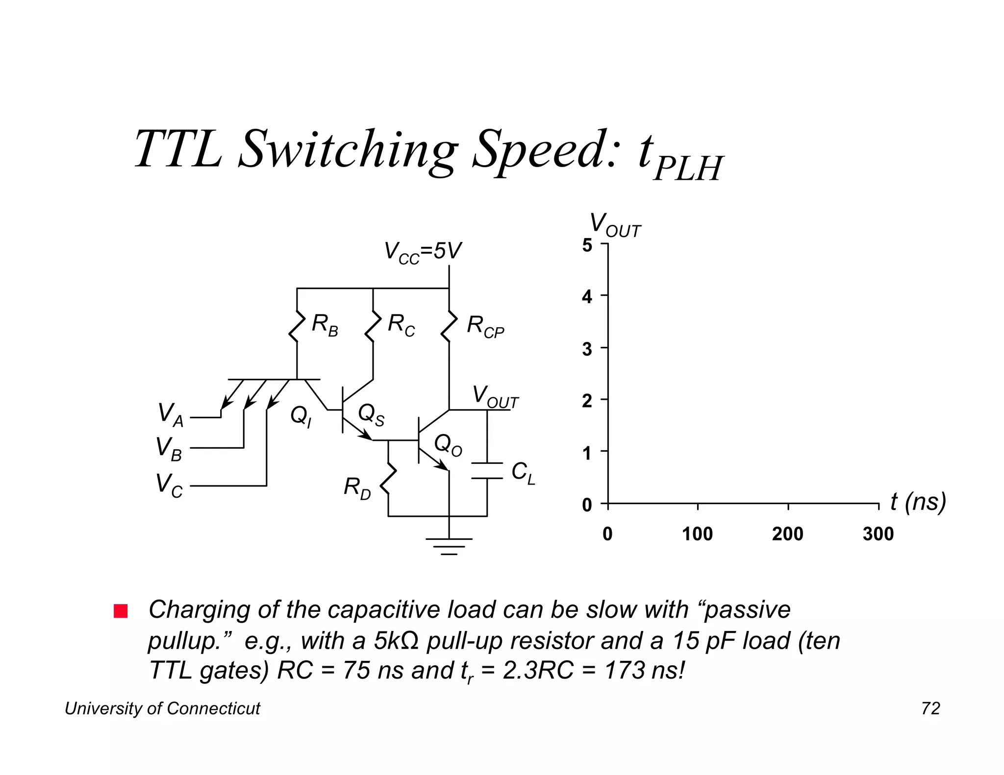
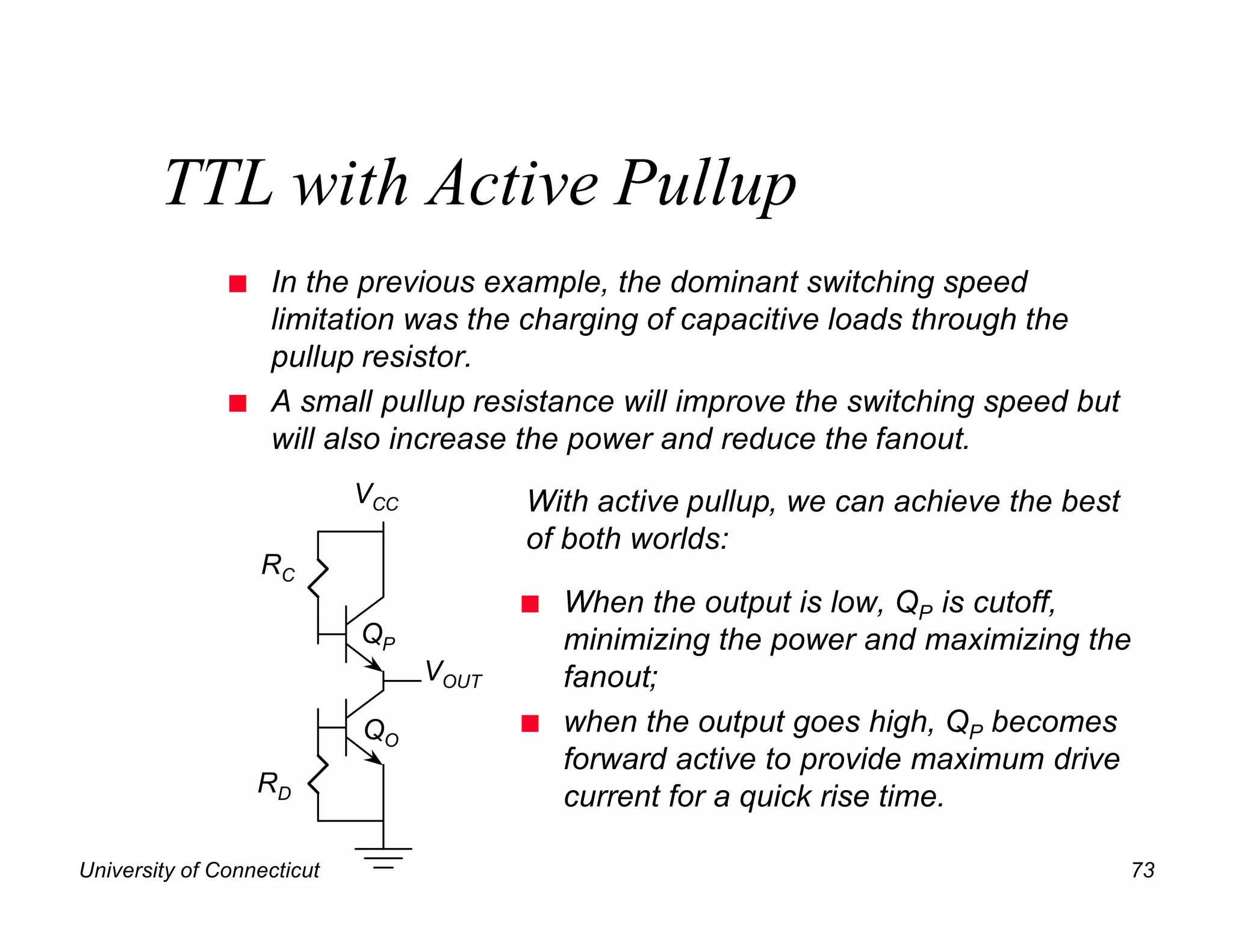
Delay analysis, improvements in switching times with active pullup circuits, and challenges associated with passive designs.
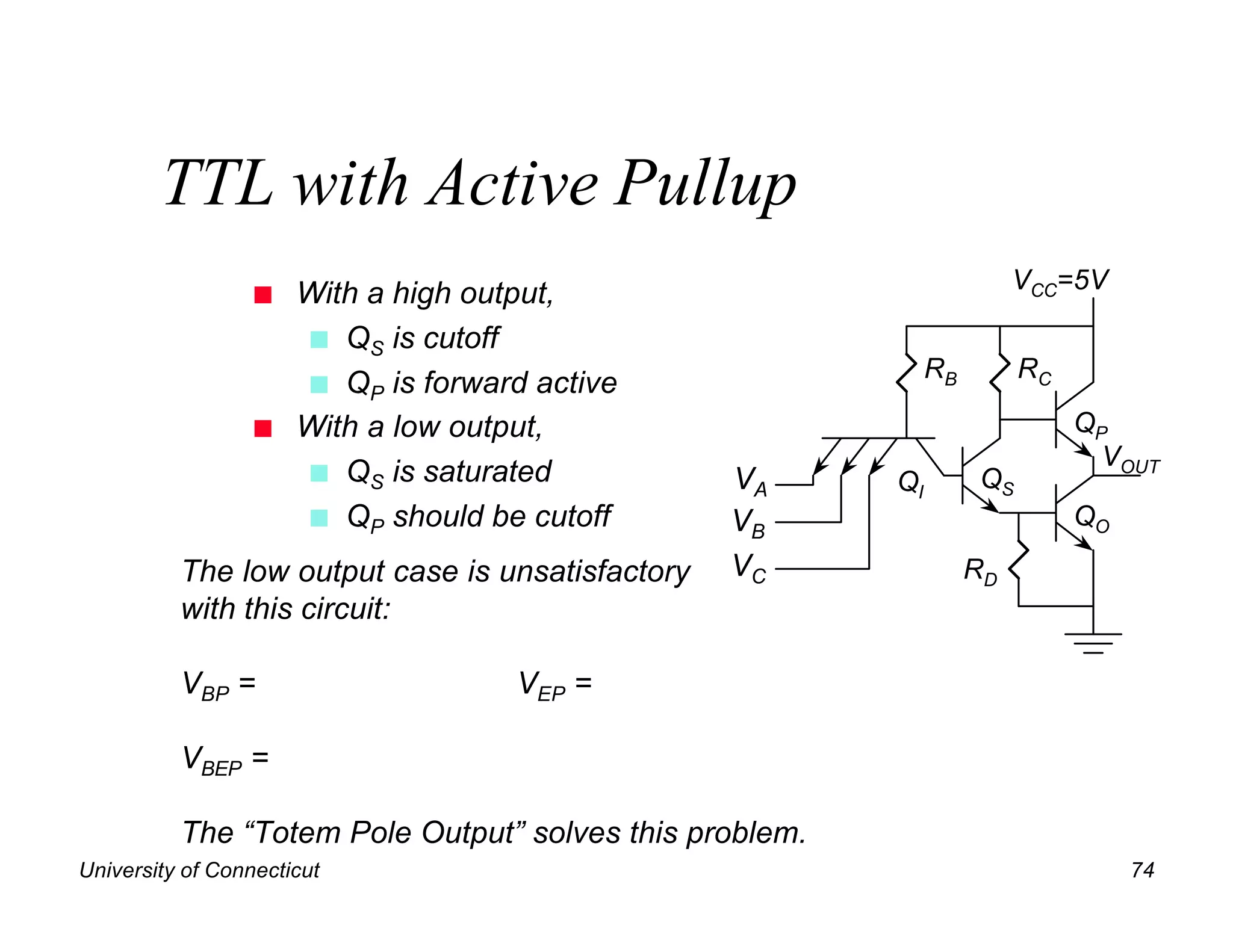
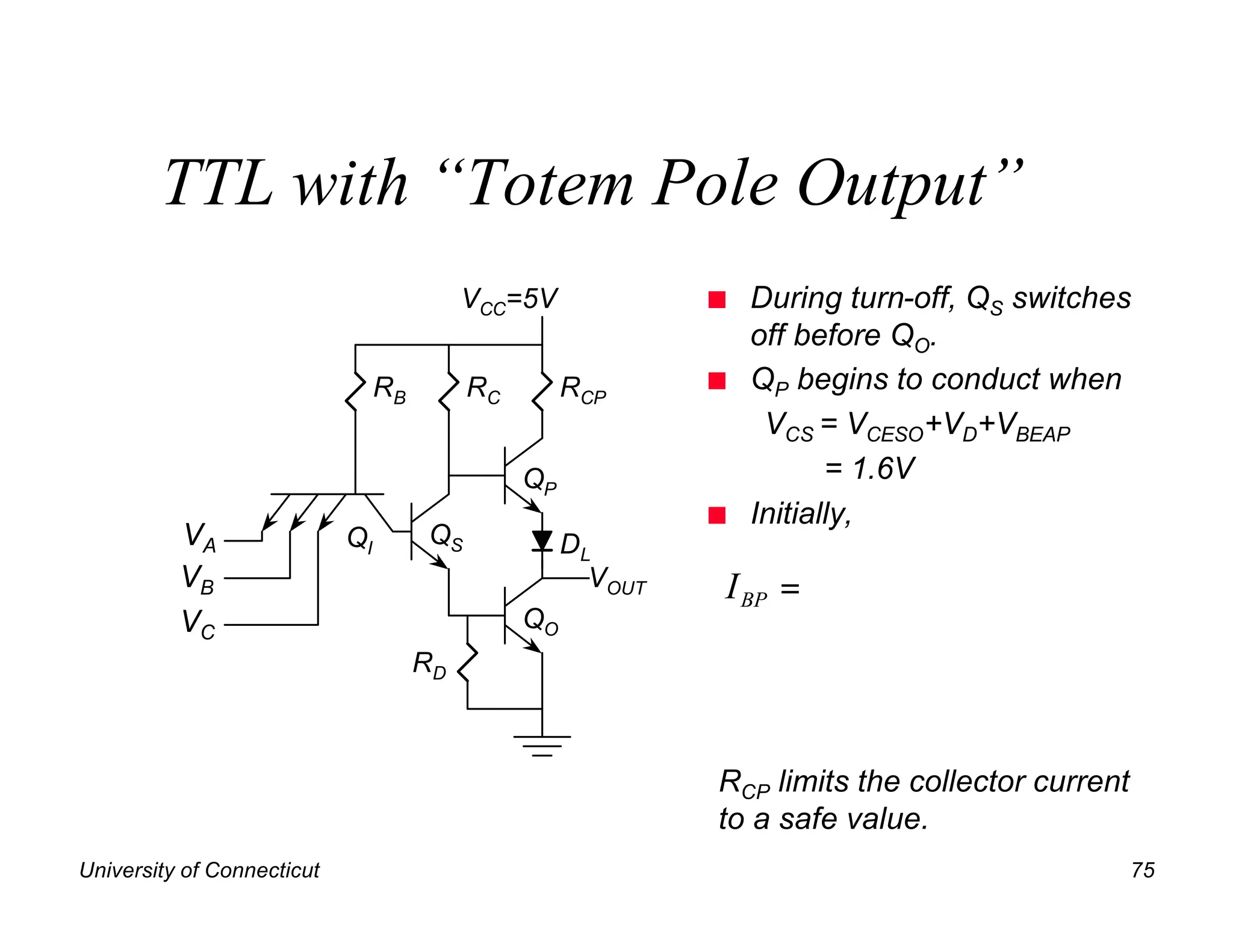
Explanation of totem pole output design, turn-off characteristics, and implications for switching performance.
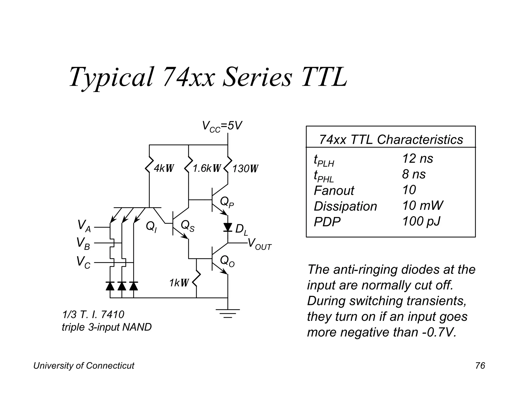
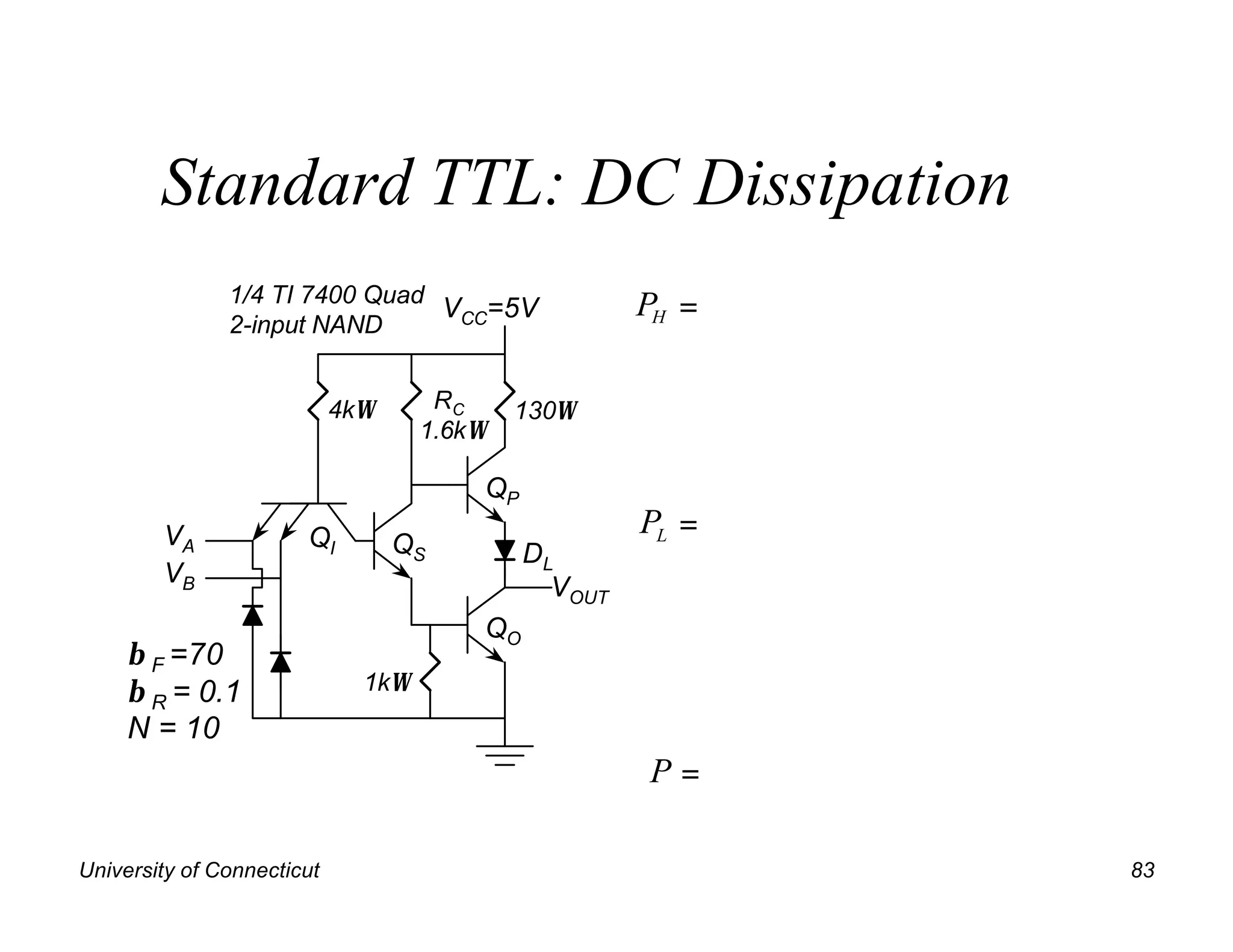
Typical specifications for 74xx series TTL, focusing on propagation delays, input currents, fanout, and dissipation.
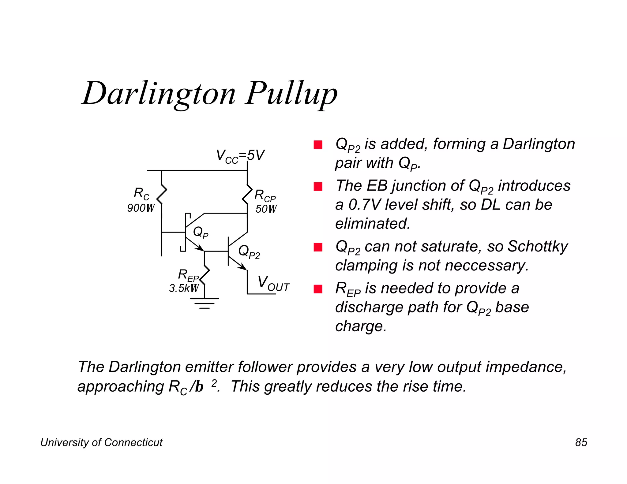
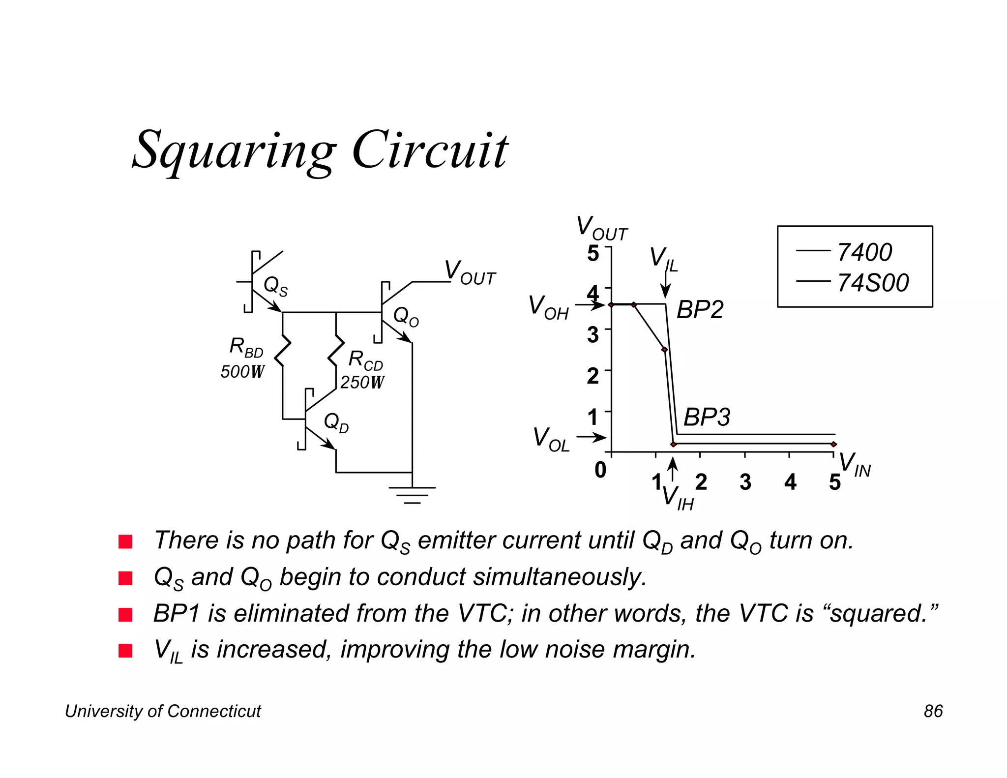
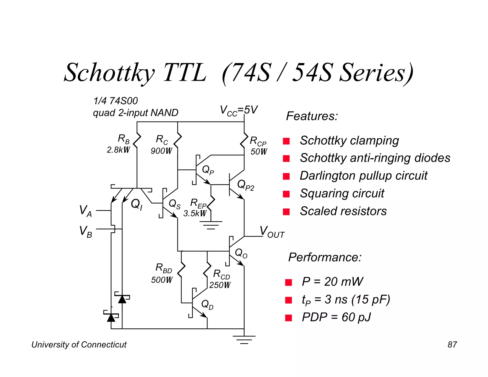
Innovations in TTL designs including Schottky clamping, Darlington pullups, squaring circuits, and details about the Schottky series.