This document discusses ripple counters and their characteristics:
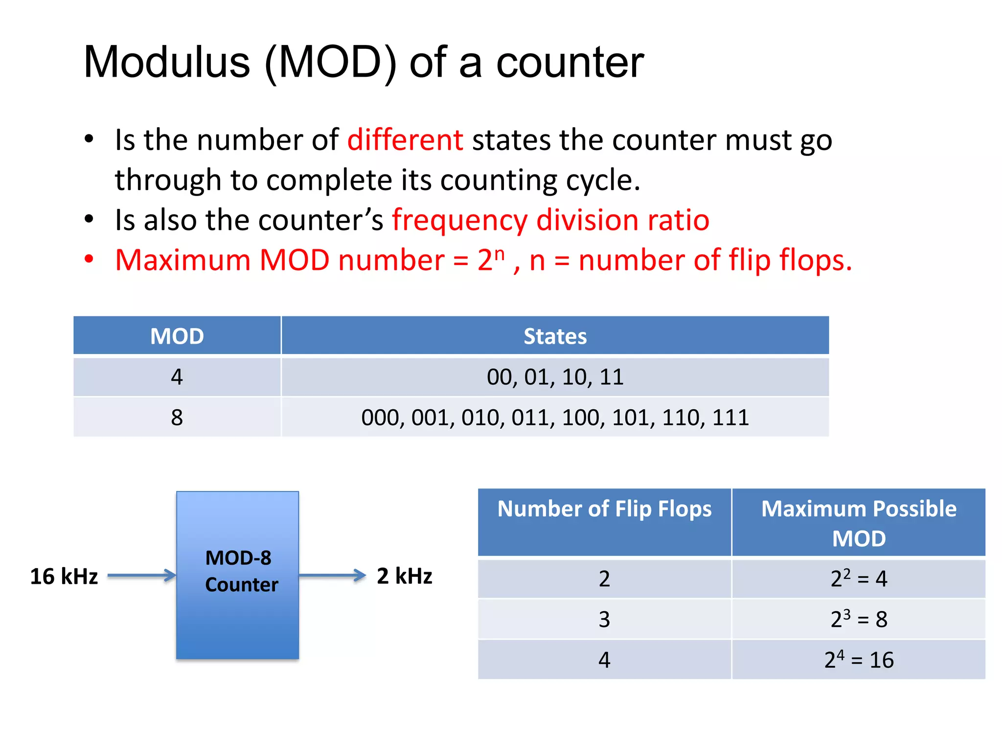
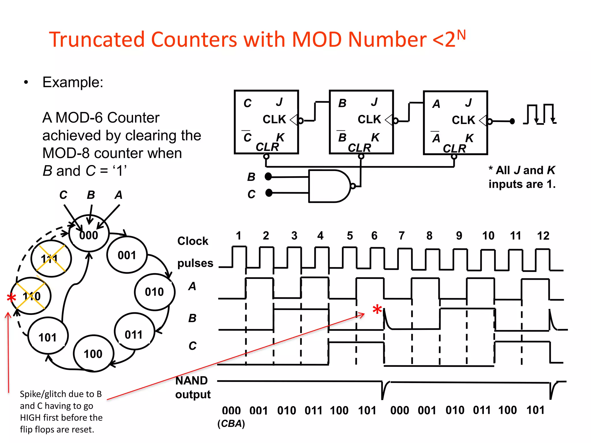
- Ripple counters have a modulus (MOD) which is the number of states the counter cycles through before repeating. The MOD is equal to 2n where n is the number of flip-flops.
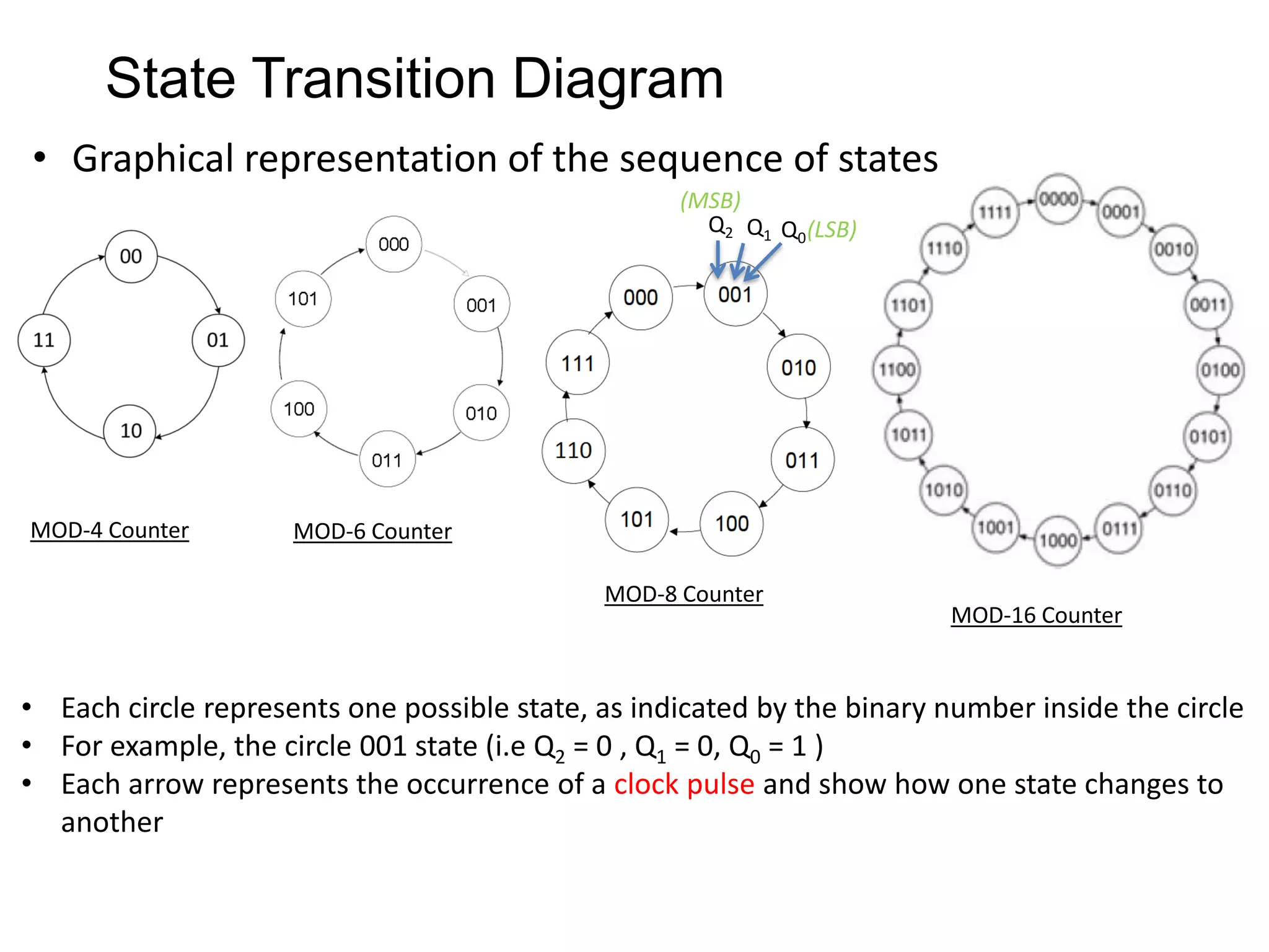
- State transition diagrams graphically represent the sequence of states a counter goes through with each clock pulse.
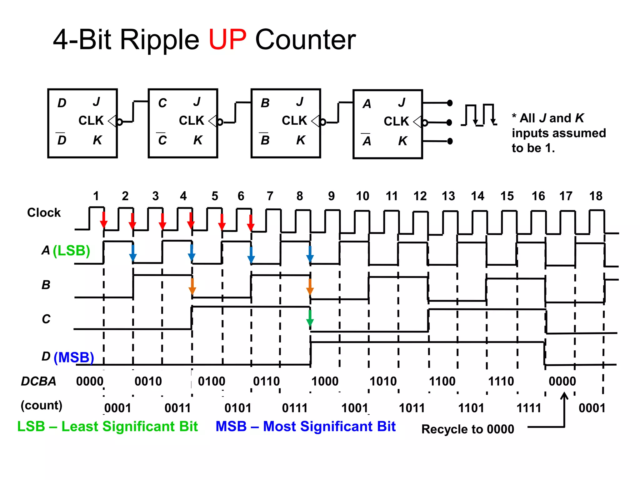
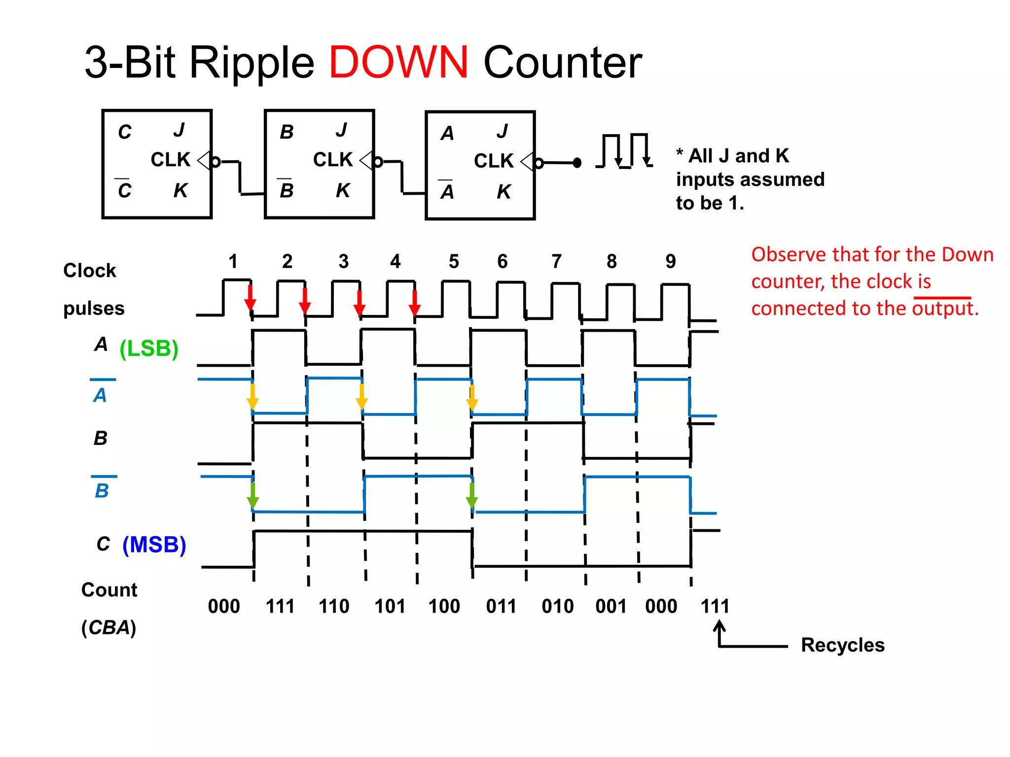
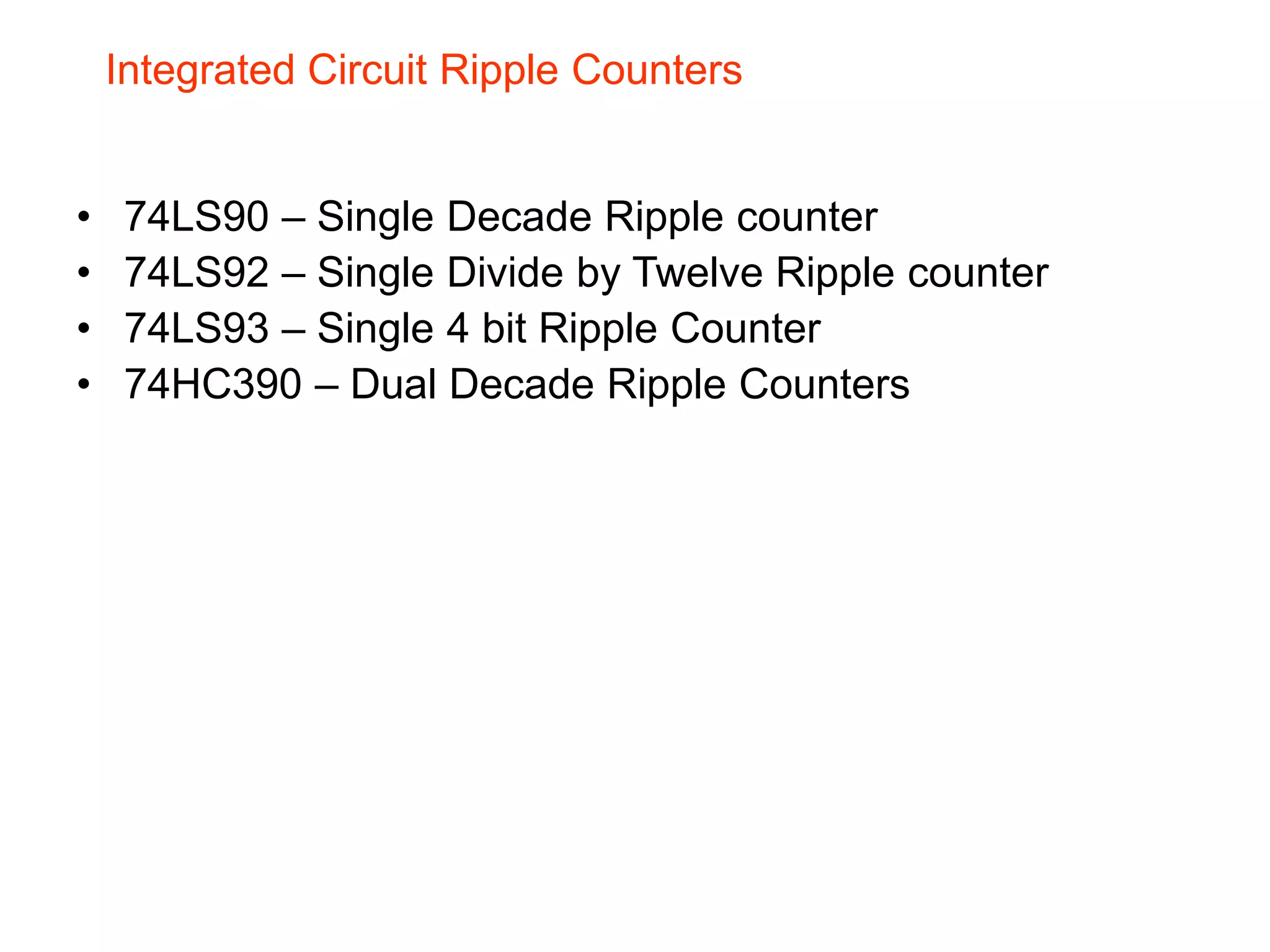
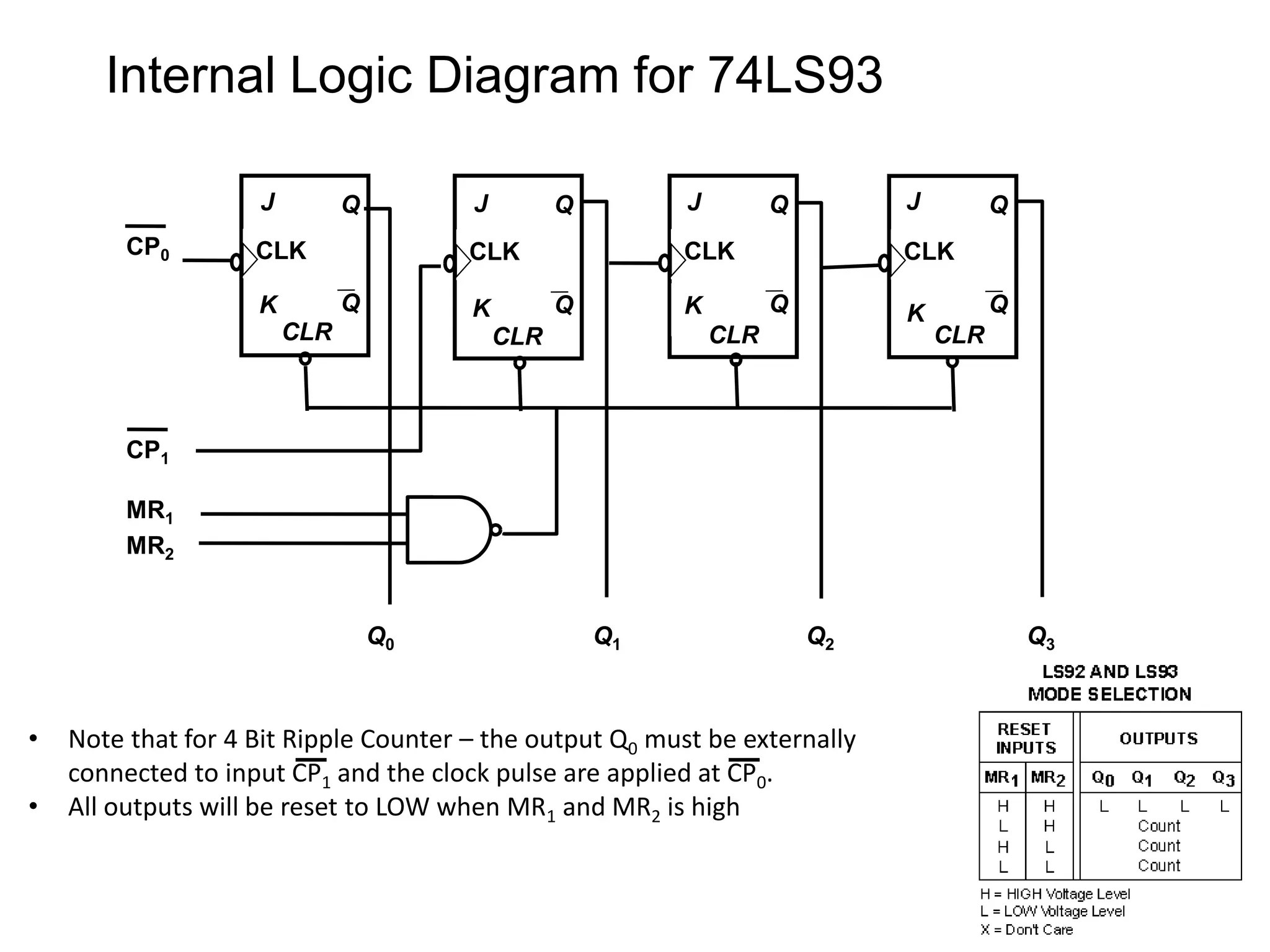
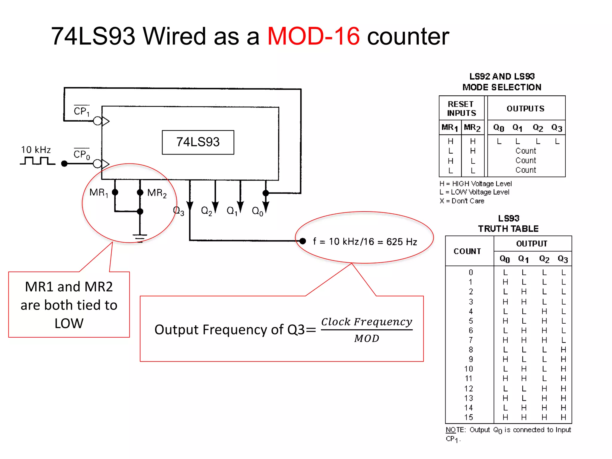
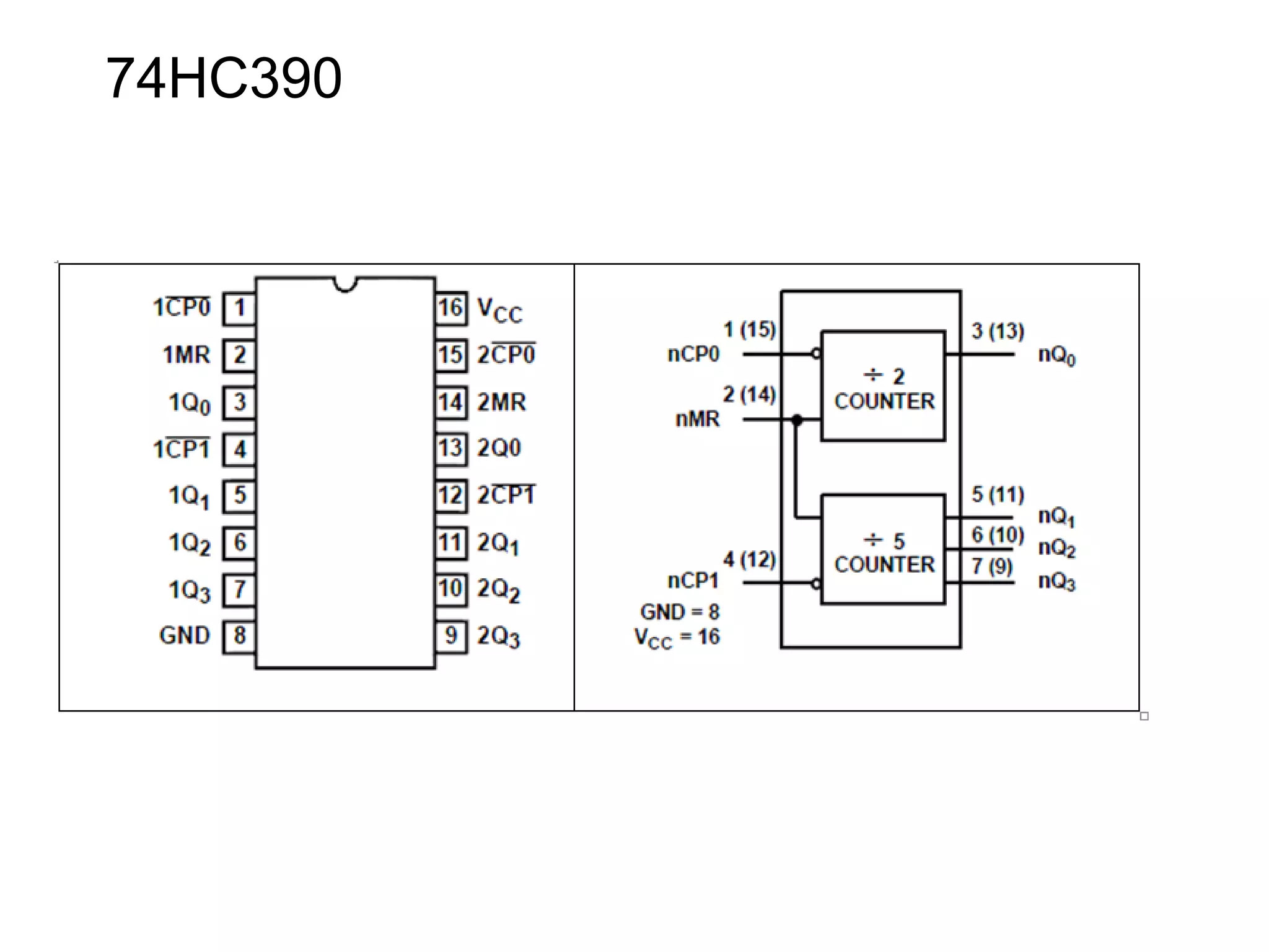
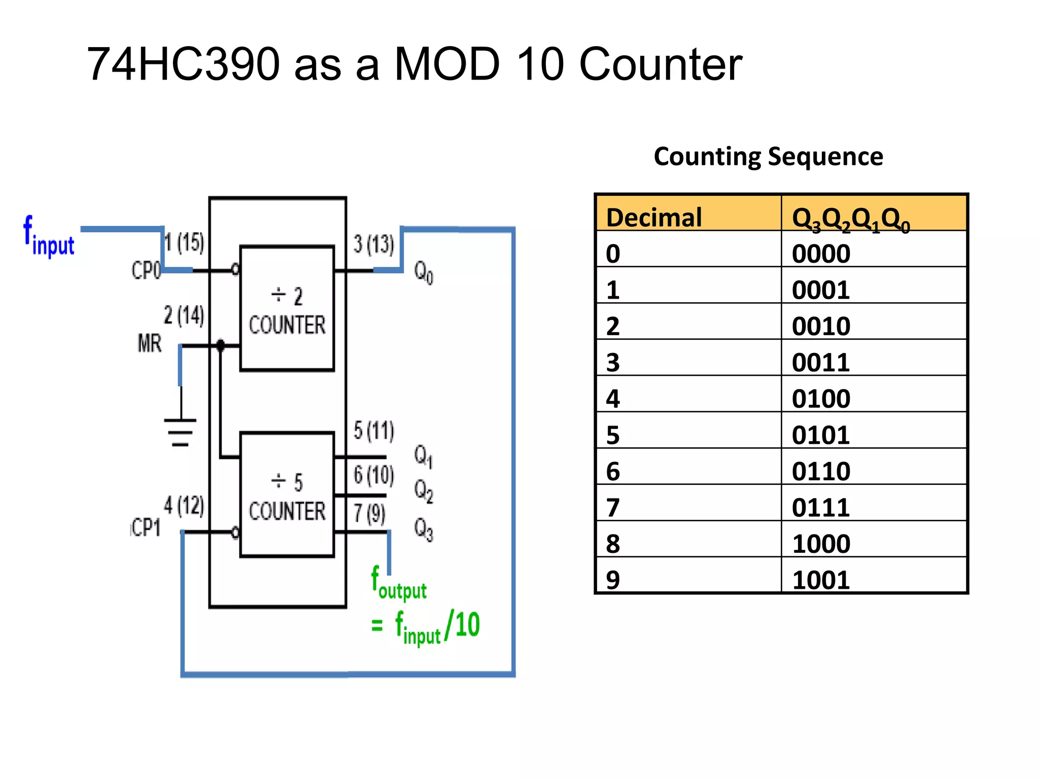
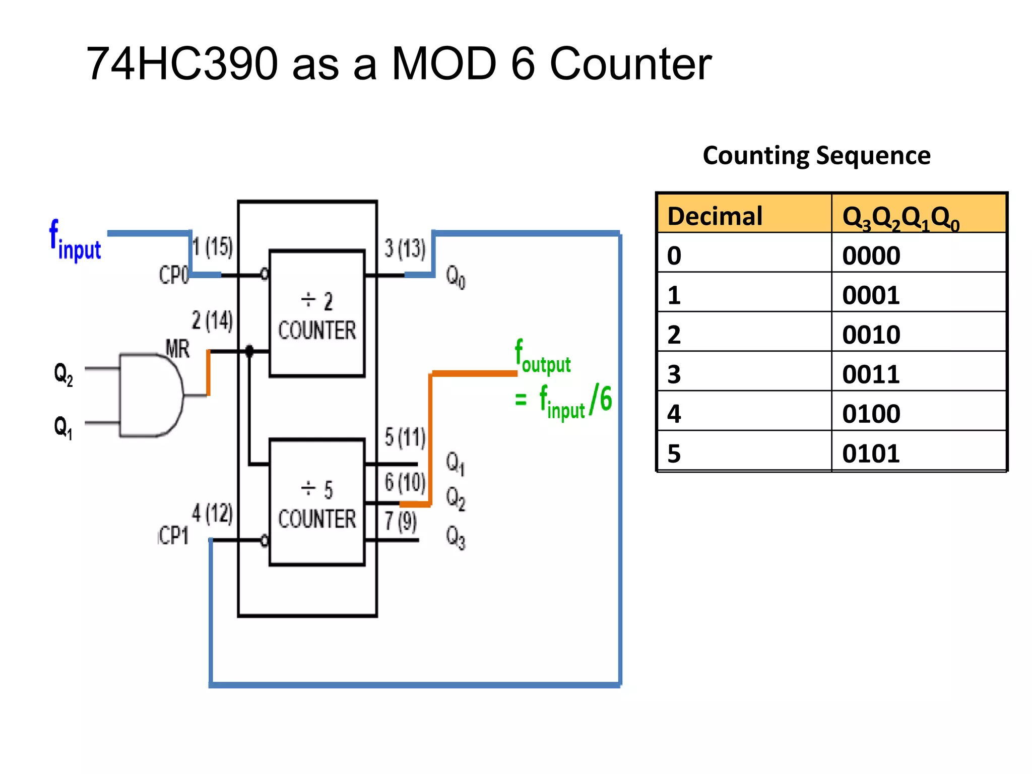
- Common integrated circuits used for ripple counters include the 74LS90, 74LS92, 74LS93 and 74HC390. The 74LS93 and 74HC390 can be configured to count to different MODs by controlling enable inputs.
- The internal logic of the 74LS93 is shown, with the clock pulse applied to


![COUNTERS [Synchronous and Asynchronous]](https://cdn.slidesharecdn.com/ss_thumbnails/counters-211217083059-thumbnail.jpg?width=640&height=640&fit=bounds)