


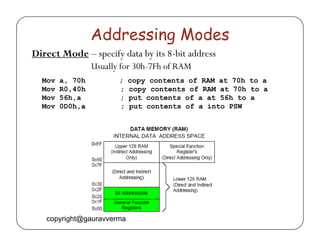
![8051 Addressing Modes
y The CPU can access data in various
ways, which are called addressing
modes.
1.Immediate
2.Register
3.Direct
4.Register indirect
5.External Direct
[label : ] mnemonic [operands] [;comment]
34
copyright@gauravverma](https://image.slidesharecdn.com/8051microcontrollerforslideshare-140905082557-phpapp01/85/8051-microcontroller-34-320.jpg)


![Addressing Modes
Register Indirect – the address of the source or destination is specified
in registers
Uses registers R0 or R1 for 8-bit address:
mov psw, #0 ; use register bank 0
mov r0, #3Ch
mov @r0, #3 ; memory at 3C gets #3
; M[3C] Å 3
Uses DPTR register for 16-bit addresses:
mov dptr ; Å 9000h
3C
r0
3
dptr, #9000h dptr 3C
movx a, @dptr ; a Å M[9000]
N t th t 9000 i dd i t l
9000
acc
xx
Note that is an address in external memory
dptr 9000
39 copyright@gauravverma](https://image.slidesharecdn.com/8051microcontrollerforslideshare-140905082557-phpapp01/85/8051-microcontroller-39-320.jpg)
![Addressing Modes
Register Indexed Mode – source or destination address is
the sum of the base address and the accumulator(Index)
y Base address can be DPTR or PC
mov dptr, #4000h
mov a, #5
movc a, @a + dptr ;a Å M[4005]
40 copyright@gauravverma](https://image.slidesharecdn.com/8051microcontrollerforslideshare-140905082557-phpapp01/85/8051-microcontroller-40-320.jpg)
![Addressing Modes
Register Indexed Mode continue
y Base address can be DPTR or PC
ORG 1000h
1000 mov a, #5
1002 movc a, @a + PC ;a Å M[1008]
PC
1003 Nop
y MOVC only can read internal or external (if connected) code
memory.
41 copyright@gauravverma](https://image.slidesharecdn.com/8051microcontrollerforslideshare-140905082557-phpapp01/85/8051-microcontroller-41-320.jpg)


![Exchange Instructions
two way data transfer
XCH a, 30h ; a ÅÆ M[30]
XCH a, R0 ; a ÅÆ R0
XCH a, @R0 ; a ÅÅÆÆ M[R0]
XCHD a, R0 ; exchange “digit”
a[7..4] a[3..0] R0[7..4] R0[3..0]
Only 4 bits exchanged
44 copyright@gauravverma](https://image.slidesharecdn.com/8051microcontrollerforslideshare-140905082557-phpapp01/85/8051-microcontroller-44-320.jpg)


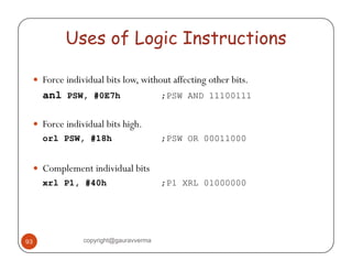
![Address Modes with Logic
ANL – AND
a, byte
[direct, reg. indirect, reg,
immediate]
ORL – OR
XRL – eXclusive oR
byte, a
[direct]
byte, #constant
a ex: cpl a CPL – Complement
92 copyright@gauravverma](https://image.slidesharecdn.com/8051microcontrollerforslideshare-140905082557-phpapp01/85/8051-microcontroller-92-320.jpg)


![Stack
y Stack-oriented data transfer
yy Only one operand (direct addressing)
y SP is other operand – register indirect - immediate
y Direct addressing mode must be used in Push
and Pop
mov sp,#40h ; Initialize SP
push 55h ; SP Å SP+1, M[SP] Å M[55]
; M[41] Å M[55]
pop b ; b Å M[55], SP Å SP-1
Note: can only specify RAM or SFRs (direct mode) to
push or pop. Therefore, to push/pop the accumulator,
must use acc, not a
102 copyright@gauravverma](https://image.slidesharecdn.com/8051microcontrollerforslideshare-140905082557-phpapp01/85/8051-microcontroller-102-320.jpg)


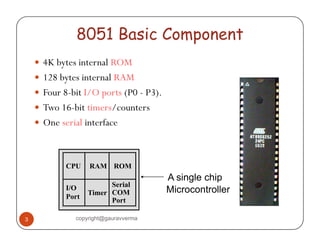
This document provides an overview of the 8051 microcontroller architecture. It describes the basic components of the 8051 including 4K bytes of internal ROM, 128 bytes of internal RAM, four 8-bit I/O ports, two timers/counters, one serial interface, and other features. It also discusses the different addressing modes for 8051 assembly language programming including immediate, register, direct, register indirect, and external direct addressing.