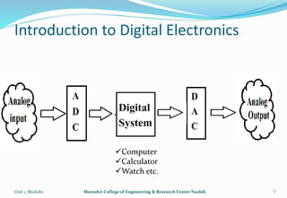
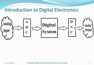
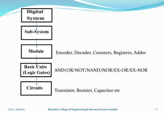
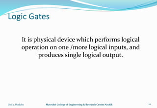
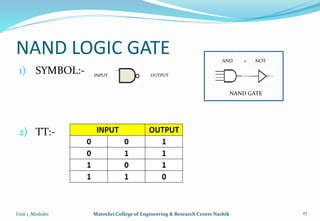
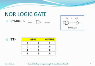
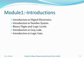
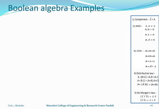
2. 203143: Analog And Digital Electronics
Teaching Scheme
Lecture : 03 Hrs/ Week
Practical : 02 Hrs/ Week
Credits
Th: 03
PR:01
Examination Scheme [Marks]
In Sem : 30 Marks
End Sem : 70 Marks
Practical : 50 Marks
Unit 1_Module1 Matoshri College of Engineering & Research Center Nashik 2
3. Course Objective
1) To use K map for Boolean algebra reduction and design digital
circuit
2) To introduce digital memories and logical families.
3) To construct sequential and combinational circuits using flip
flops and K map
4) To develop the concept of basics of operational Amplifier and
its applications.
5) To design uncontrolled rectifier
4. Course Outcomes
Upon successful completion of this course, the students will be
able to :-
CO1: Design logical, sequential and combinational digital circuit
using K-Map.
CO2: Demonstrate different digital memories and programmable
logic families.
CO3: Apply and analyze applications of OPAMP in open and closed
loop condition.
CO4: Design uncontrolled rectifier with given specifications
5. Unit 01 : Design of combinational circuit
M1:-Introductions
M2:- Booleans algebra, De-Morgan theory.
M3:- Karnaugh map: structure for two, three and four Variables, SOP and
POS form reduction of Boolean expressions by K-map.
M4:- Design of combinational circuits using Boolean expression and K-
map.
M5:- encoder, decoder, half and full adder.
Unit 1_Module1 Matoshri College of Engineering & Research Center Nashik 5
6. Module1:-Introductions
Introduction to Digital Electronics.
Introduction to Number System.
Binary Digits and Logic Levels.
Introduction to Gray code.
Binary Digits and Logic Levels.
Unit 1_Module1 Matoshri College of Engineering & Research Center Nashik 6
7. Introduction to Digital Electronics
Unit 1_Module1 Matoshri College of Engineering & Research Center Nashik 7
Computer
Calculator
Watch etc.
9. Introduction to Digital Electronics
Unit 1_Module1 Matoshri College of Engineering & Research Center Nashik 9
10. Unit 1_Module1 Matoshri College of Engineering & Research Center Nashik 10
Transistor, Resister, Capacitor etc
AND/OR/NOT/NAND/NOR/EX-OR/EX-NOR
Encoder, Decoder, Counters, Registers, Adder
11. Number system define a set of value used to represent
quantity
NAME BASE (Radix)
Decimal 10
Binary 2
Octal 8
Hexadecimal 16
INTRODUCTION TO NUMBER SYSTEM
12. Decimal number system
Name Base (radix) Characters in set
Decimal 10 0,1,2,3,4,5,6,7,8,9
0 to (r-1)
0 to (10-1)
0 to 9
7 3 9 2 . 9 1
.
13. Binary number system
Name Base (radix) Characters in set
Binary 2 0,1
0 to (r-1)
0 to (2-1)
0 to 1
1 0 0 1 . 1 0 1
.
14. Octal number system
Name Base (radix) Characters in set
Octal 8 0,1,2,3,4,5,6,7
0 to (r-1)
0 to (8-1)
0 to 7
5 6 3 2 . 4 7 1
.
15. Hexadecimal number system
Name Base (radix) Characters in set
Hexadecimal 16 0,1,2,3,4,5,6,7,8,9,A,B,C,D,E,F
0 to (r-1)
0 to (16-1)
0 to 15
10=A
11=B
12=C
13=D
14=E
15=F
3 F D . 8 4
.
16. System Base Symbols
Used by
humans?
Used in
computers?
Decimal 10 0,1,2,3,4,5,6,7,8,9 Yes No
Binary 2 0, 1 No Yes
Octal 8 0,1,2,3,4,5,6,7 No No
Hexa-
decimal
16
0,1,2,3,4,5,6,7,8,9,
A,B,C,D,E,F
No No
17. Binary Digits and Logic Levels
Digital electronics uses circuits that have two states, which
are represented by two different voltage levels called HIGH
and LOW. The voltages represent numbers in the binary
system.
Unit 1_Module1 Matoshri College of Engineering & Research Center Nashik 17
A bit can have the value
of either 0 or 1,
depending on if the
voltage is HIGH or LOW.
0 volt
2 volt
3 volt
5 volt
18. Digital waveforms change between the LOW and HIGH levels. A
positive going pulse is one that goes from a normally LOW logic
level to a HIGH level and then back again. Digital waveforms are
made up of a series of pulses.
Unit 1_Module1 Matoshri College of Engineering & Research Center Nashik 18
Digital Waveforms
19. Introduction to gray code
Its also known as “Reflected binary code” (RBC)
Invented by frank gray
Its Unweighted code
In gray code , “Two successive values differ in only 1 bit”
Unit 1_Module1 Matoshri College of Engineering & Research Center Nashik 19
Frank gray
22. Logic Gates
Unit 1_Module1 Matoshri College of Engineering & Research Center Nashik 22
It is physical device which performs logical
operation on one /more logical inputs, and
produces single logical output.
23. Classification of Logic Gates
Logic Gates
Basic Logic Gates
OR NOT AND
Universal Logic Gates
NAND NOR
Special Logic Gates
EX-OR EX-NOR
Unit 1_Module1 Matoshri College of Engineering & Research Center Nashik 23
26. OR LOGIC GATE
1) SYMBOL:-
2) TT:-
Unit 1_Module1 Matoshri College of Engineering & Research Center Nashik 26
INPUT OUTPUT
27. NAND LOGIC GATE
1) SYMBOL:-
2) TT:-
Unit 1_Module1 Matoshri College of Engineering & Research Center Nashik 27
INPUT OUTPUT
AND + NOT
NAND GATE
28. NOR LOGIC GATE
1) SYMBOL:-
2) TT:-
Unit 1_Module1 Matoshri College of Engineering & Research Center Nashik 28
INPUT OUTPUT
OR + NOT
NOR GATE
29. Module1:-Introductions
Introduction to Digital Electronics.
Introduction to Number System.
Binary Digits and Logic Levels.
Introduction to Gray code.
Introduction to Logic Gate.
Unit 1_Module1 Matoshri College of Engineering & Research Center Nashik 29
31. Thank you
Mr. C. R. Shinde
Electrical Engineering Department
Matoshri College of Engineering & Research centre, Nashik
If you have any query, ask me anytime on…… … .. . . .
cshinde58@gmail.com
chandrakant.shinde@matoshri.edu.in
9970031353
Unit 1_Module1 Matoshri College of Engineering & Research Center Nashik 31
33. Introduction to Booleans algebra
It is set of rules, used to simplify the given logic
expression without changing its functionality
It is used when number of variables less
Unit 1_Module1 Matoshri College of Engineering & Research Center Nashik 33
George Boole
1815-1864
NOT
AND AND AND
OR
NEED 5 LOGIC GATES
NOT
AND AND
OR
NEED 4 LOGIC GATES