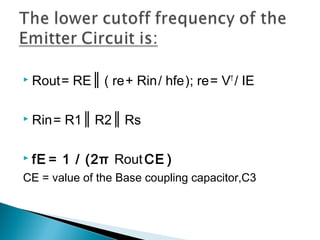
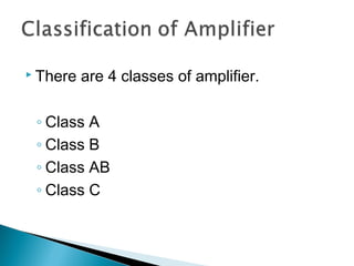
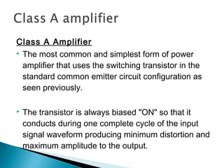
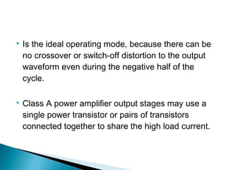
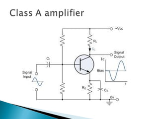
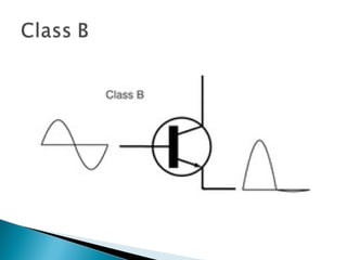
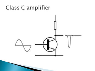
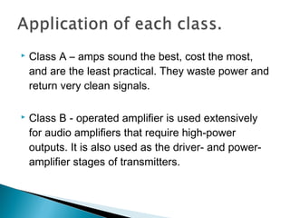
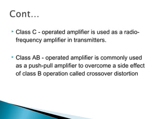
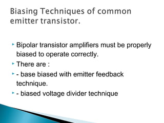
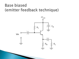
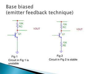
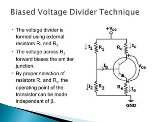
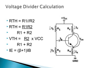
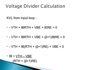
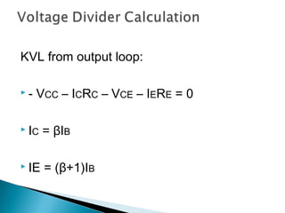
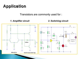
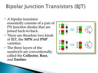
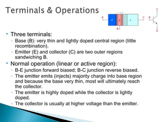
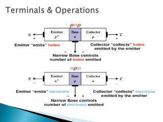
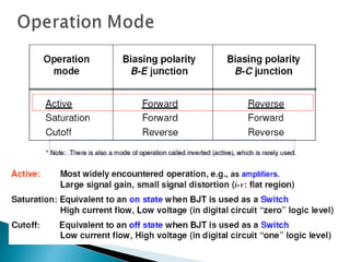
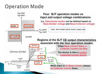
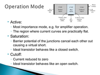
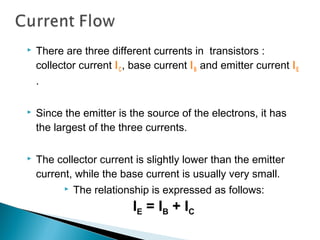
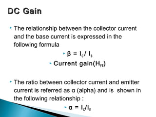
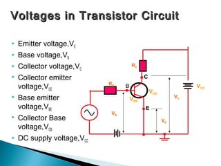
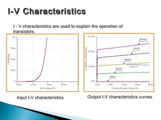
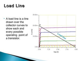
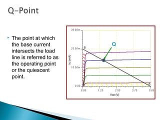
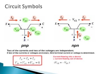
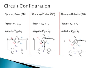
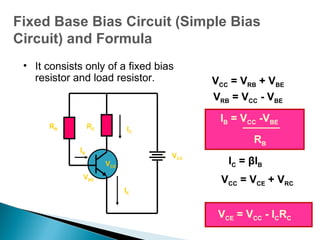
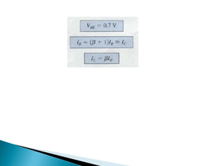
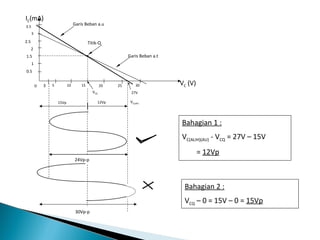
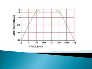
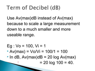
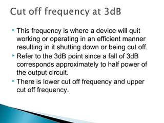
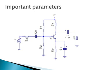
This document discusses bipolar junction transistors (BJTs). It describes the basic structure and operation of NPN and PNP BJTs, including their three terminals (base, emitter, collector), current flow, and biasing. BJTs can be used as switches in digital circuits or amplifiers in analog circuits. The document also covers BJT characteristics such as active, saturation, and cutoff regions; DC current gains; and voltage relationships. BJT amplifier classes like Class A, B, AB, and C are introduced along with their relative efficiencies. Stabilization techniques for BJT amplifiers using emitter feedback and voltage divider biasing are also summarized.
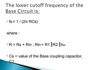
The study of the basics of electronics can be studied through the link http://bit.ly/2PPv0mv
The transistor is a semiconductor device with three connections, capable of amplification in addition to rectification
Its looks like a letter Z due to symmetrical switching characteristics for each polarity of the applied voltage. ... This means that, unlike the triac and the SCR, the disc cannot be estimated to maintain a low voltage drop until its current falls below the level of holding current. A triac is a 4-layer semiconductor device with two power terminals (MT1 and MT2) and a gate terminal. It is used as a power control device for 50/60Hz AC mains applications. It is placed in series with the load connected across the mains. ... A disc is a similar 4-layer device but does not have a gate terminal.
http://bit.ly/2PIOIQM
EST 130, Transistor Biasing and Amplification.CKSunith1
The attached narrated power point presentation explains the need for biasing in transistor amplifiers and the different biasing arrangements used in transistor circuits. The material will be useful for KTU first year B Tech students who prepare for the subject EST 130, Part B, Basic Electronics Engineering.
single phase half bridge inverter, full bridge inverter, parallel inverter, load commutated inverter with working and waveforms.
download and watch the animations. it will be effective.
single phase bridge inverter harmonic analysis.
Objectives
Understand the concept of amplifiers
Identify and apply internal transistor parameters
Understand and analyze common-emitter, common-collector and common-base amplifiers
Introduction
One of the primary uses of a transistor is to amplify ac signals. It has to be able to do it without distorting the original input.
Amplifier
The collector curves and load lines help us to relate the Q-point and its proximity to cutoff and saturation. The Q-point is best established where the signal variations do not cause the transistor to go into saturation or cutoff. For perfect amplifier Q-point must be in the middle of the active region.
Amplifier Operation
The region between cutoff and saturation is called the linear region. A transistor which operates in the linear region is called a linear amplifier. Note that only the ac component reaches the load because of the capacitive coupling and that the output is 180º out of phase with input.
The Common-Emitter Amplifier
The common-emitter amplifier exhibits high voltage gain and current gain. The output signal is 180º out of phase with the input signal.
Characteristics
Voltage gain -High
Current gain - High
Power gain - High
Input or output phase relationship - 180 degree
Input resistance - Low
Output resistance -High
Introduction to feedback (block diagram and types of feedback) , Analysis at middle, low and high frequency of multi-stage amplifier with RC coupling and direct coupling, cascade amplifiers-Darlington Pair.
discussing differences faithful and un- faithful amplification
discussing stabilition in transistors
and how temperature affect collector current
discussing various methods of transistor biasing like
Base resister method ,Emitter Base method , Biasing with collector feedback method , Voltage divider bias
Electrical current, voltage, resistance, capacitance, and inductance are a few of the basic elements of electronics and radio. Apart from current, voltage, resistance, capacitance, and inductance, there are many other interesting elements to electronic technology. ... Use Electronics Notes to learn electronics online.
The French Revolution, which began in 1789, was a period of radical social and political upheaval in France. It marked the decline of absolute monarchies, the rise of secular and democratic republics, and the eventual rise of Napoleon Bonaparte. This revolutionary period is crucial in understanding the transition from feudalism to modernity in Europe.
For more information, visit-www.vavaclasses.com
Palestine last event orientationfvgnh .pptxRaedMohamed3
An EFL lesson about the current events in Palestine. It is intended to be for intermediate students who wish to increase their listening skills through a short lesson in power point.
Biological screening of herbal drugs: Introduction and Need for
Phyto-Pharmacological Screening, New Strategies for evaluating
Natural Products, In vitro evaluation techniques for Antioxidants, Antimicrobial and Anticancer drugs. In vivo evaluation techniques
for Anti-inflammatory, Antiulcer, Anticancer, Wound healing, Antidiabetic, Hepatoprotective, Cardio protective, Diuretics and
Antifertility, Toxicity studies as per OECD guidelines
Read| The latest issue of The Challenger is here! We are thrilled to announce that our school paper has qualified for the NATIONAL SCHOOLS PRESS CONFERENCE (NSPC) 2024. Thank you for your unwavering support and trust. Dive into the stories that made us stand out!
How to Make a Field invisible in Odoo 17Celine George
It is possible to hide or invisible some fields in odoo. Commonly using “invisible” attribute in the field definition to invisible the fields. This slide will show how to make a field invisible in odoo 17.
Instructions for Submissions thorugh G- Classroom.pptxJheel Barad
This presentation provides a briefing on how to upload submissions and documents in Google Classroom. It was prepared as part of an orientation for new Sainik School in-service teacher trainees. As a training officer, my goal is to ensure that you are comfortable and proficient with this essential tool for managing assignments and fostering student engagement.
Honest Reviews of Tim Han LMA Course Program.pptxtimhan337
Personal development courses are widely available today, with each one promising life-changing outcomes. Tim Han’s Life Mastery Achievers (LMA) Course has drawn a lot of interest. In addition to offering my frank assessment of Success Insider’s LMA Course, this piece examines the course’s effects via a variety of Tim Han LMA course reviews and Success Insider comments.
Introduction to AI for Nonprofits with Tapp NetworkTechSoup
Dive into the world of AI! Experts Jon Hill and Tareq Monaur will guide you through AI's role in enhancing nonprofit websites and basic marketing strategies, making it easy to understand and apply.
2. Two main categories of transistors:
◦ bipolar junction transistors (BJTs) and
◦ field effect transistors (FETs).
Transistors have 3 terminals where the application of
current (BJT) or voltage (FET) to the input terminal
increases the amount of charge in the active region.
The physics of "transistor action" is quite different for the
BJT and FET.
In analog circuits, transistors are used in amplifiers and
linear regulated power supplies.
In digital circuits they function as electrical switches,
including logic gates, random access memory (RAM),
and microprocessors.
3. A bipolar transistor
essentially consists of a pair of
PN Junction diodes that are
joined back-to-back.
There are therefore two kinds
of BJT, the NPN and PNP
varieties.
The three layers of the
sandwich are conventionally
called the Collector, Base,
and Emitter.
4. Three terminals:
◦ Base (B): very thin and lightly doped central region (little
recombination).
◦ Emitter (E) and collector (C) are two outer regions
sandwiching B.
Normal operation (linear or active region):
◦ B-E junction forward biased; B-C junction reverse biased.
◦ The emitter emits (injects) majority charge into base region
and because the base very thin, most will ultimately reach
the collector.
◦ The emitter is highly doped while the collector is lightly
doped.
◦ The collector is usually at higher voltage than the emitter.
5.
6.
7.
8. Active:
◦ Most importance mode, e.g. for amplifier operation.
◦ The region where current curves are practically flat.
Saturation:
◦ Barrier potential of the junctions cancel each other out
causing a virtual short.
◦ Ideal transistor behaves like a closed switch.
Cutoff:
◦ Current reduced to zero
◦ Ideal transistor behaves like an open switch.
9. There are three different currents in transistors :
collector current I C , base current I B and emitter current I E
.
Since the emitter is the source of the electrons, it has
the largest of the three currents.
The collector current is slightly lower than the emitter
current, while the base current is usually very small.
The relationship is expressed as follows:
IE = IB + IC
10. DC Gain
The relationship between the collector current
and the base current is expressed in the
following formula
β = I / I
C B
Current gain(H FE )
The ratio between collector current and emitter
current is referred as α (alpha) and is shown in
the following relationship :
α = I /I
C E
11. Voltages in Transistor Circuit
Emitter voltage,VE
Base voltage,VB
Collector voltage,VC RC
Collector emitter C
RB
voltage,VCE B VCC
VCE
Base emitter VBE VC
voltage,VBE E
VB
Collector Base VE
voltage,VCB
DC supply voltage,VCC
12. I-V Characteristics
I - V characteristics are used to explain the operation of
transistors.
Input I-V characteristics Output I-V characteristics curves
13. Load Line
A load line is a line
drawn over the
collector curves to
show each and
every possible Lo
operating point of a dl
ine
a transistor.
14. The point at which
the base current Q
intersects the load
line is referred to as
the operating point
or the quiescent
point.
15.
16.
17. Fixed Base Bias Circuit (Simple Bias
Circuit) and Formula
• It consists only of a fixed bias
resistor and load resistor. VCC = VRB + VBE
VRB = VCC - VBE
IB = VCC -VBE
RB RC IC
RB
IB
VCC
VCE IC = βIB
VBE VCC = VCE + VRC
IE
VCE = VCC - ICRC
18.
19. Potential Divider Bias Circuit
It offers the best resilience against
changes in temperature and device
characteristics and by far more stabilized.
R1 RC R1 and R2 form a potential divider, which
IC
will fix the base potential of the transistor.
IB The current is usually set at 10 times
VCC greater than the base current required by
VCE the transistor
VBE
The base emitter voltage drop is
R2 RE IE approximated as 0.7volt. There will also
be a voltage drop across the emitter
resistor, RE, this is generally set to about
10% of the supply voltage.
If IC increases, then so will IE.
20. Formula
VCC = IR1 + IR2 IE = I B + I C
VCE = VCC –VRC - VRE
VC = VCE + VRE
VB = R2 VCC
R1 + R2
VRE = VB - VBE
IE = VRE/ RE
IB can be ignored if the value is too small
21. One factor can affect the IB is AC input signal.
AC input signal must not too big so that can control the
IB.
22. IC(mA)
Q point is at IB = 60µA, Ic =
100µA
10 6mA, Vc = 8V.
80µA
8
60µA
If IB is between 40µA and
6
80µA, while Ic is between 4mA
4
40µA
and 8mA
20µA
2
So Vc is between 4V and 12V.
0V
VC (V)
4 5 8 10 12 15 20 Vc is output voltage for the
amplifier circuit, Vo.
23. If input signal is too big, It will affect the IB.
IB will become big, followed by Ic and Vc.
Ic and Vc will over the saturation point and will
cut the signal.
When this happen, there is a distortion to the
output signal.
If there is a distortion to the output signal, the
amplifier is not efficient.
24. From figure above, Load resistance,
rL : R3 // R6
Will have a new AC loadline (new value of cut off
and saturation point).
Ic(sat)new = ICQ + (VCQ/RL)
Vc(sat)new = VCQ + ICQ . RL
26. Av = Vo/Vi = rL / re
Where re = 25mV/ IE
AC loadline exists when the load for AC voltage
output is different with the load for DC voltage
output.
28. Is output voltage that oscillated within the
operation point symmetrically and no distortion.
29. Can be determine from equation Av = rL / re
Use the Av to determine maximum input voltage, Vi.
Av = Vo/Vi, so Vi = Vo/Av.
It can define as undistorted maximum input
signal because it has undistorted maximum
output signal.
30.
31.
32. Frequency response is characterized by the
response magnitude (measure in dB) versus
frequency.
From frequency response graph above :
Y – axis (shows response in decibel (dB))
X – axis (shows frequency (Hz))
Important parameters of frequency response
curve :
◦ Maximum voltage gain, Av(max).
◦ Maximum voltage gain, Av (max) in dB
◦ Cut off frequency (-3dB)
◦ Frequency bandwidth.
33. Maximum voltage gain , Av(max) =
maximum ratio of output voltage, Vo over
input voltage, Vi.
Av in dB = 20 log Av(max)
Cut off frequency – or corner frequency is
the frequency either above or below
power output of a circuit.
34. fc1 – lower 3dB cut off frequency
fc2 – upper 3dB cut off frequency
Frequency Bandwidth – range of
frequency between fc1 and fc2.
35. Use Av(max)dB instead of Av(max)
because to scale a large measurement
down to a much smaller and more
useable range.
Eg : Vo = 100, Vi = 1
Av(max) = Vo/Vi = 100/1 = 100
In dB, Av(max)dB = 20 log Av(max)
= 20 log 100 = 40.
36. This frequency is where a device will quit
working or operating in an efficient manner
resulting in it shutting down or being cut off.
Refer to the 3dB point since a fall of 3dB
corresponds approximately to half power of
the output circuit.
There is lower cut off frequency and upper
cut off frequency.
37. a band of a given width can carry the
same amount of information.
So to relate bandwidth to the
performance of amplifier,
◦ wide bandwidth, the amplifier is more
efficient.
◦ BW = fc2 – fc1
38.
39. fB = 1 / (2π RCB)
where :
R = Rs + Rin ; Rin = R1 ║R2 ║hie
CB = value of the Base coupling capacitor,
C1
40. fC = 1 / [2π (RC + RL) CC]
RC +RL = sum of the resistance in the
collector circuit
CC = value of the Base coupling capacitor,
C2
41. Rout = RE ║ ( re + Rin / hfe ); re = VT / IE
Rin = R1 ║ R2 ║ Rs
fE = 1 / (2π Rout CE )
CE = value of the Base coupling capacitor,C3
42. There are 4 classes of amplifier.
◦ Class A
◦ Class B
◦ Class AB
◦ Class C
43. Class A Amplifier
The most common and simplest form of power
amplifier that uses the switching transistor in the
standard common emitter circuit configuration as
seen previously.
The transistor is always biased "ON" so that it
conducts during one complete cycle of the input
signal waveform producing minimum distortion and
maximum amplitude to the output.
44. Is the ideal operating mode, because there can be
no crossover or switch-off distortion to the output
waveform even during the negative half of the
cycle.
Class A power amplifier output stages may use a
single power transistor or pairs of transistors
connected together to share the high load current.
45.
46. Class-B amplifiers only amplify half of the input
wave cycle, thus creating a large amount of
distortion, but their efficiency is greatly improved
and is much better than class A.
Class B has a maximum theoretical efficiency of
π/4. (i.e. 78.5%) This is because the amplifying
element is switched off altogether half of the time,
and so cannot dissipate power.
47. A single class-B element is rarely found in
practice, though it has been used for driving
the loudspeaker in the early IBM Personal
Computers with beeps, and it can be used in RF
power amplifier where the distortion levels are
less important. However, class C is more
commonly used for this.
48.
49. A practical circuit using class-B elements is
the push–pull stage, such as the very simplified
complementary pair arrangement .
Complementary or quasi-complementary devices
are each used for amplifying the opposite halves
of the input signal, which is then recombined at
the output.
50.
51.
52. This arrangement gives excellent efficiency, but
can suffer from the drawback that there is a small
mismatch in the cross-over region – at the "joins"
between the two halves of the signal, as one
output device has to take over supplying power
exactly as the other finishes. This is
called crossover distortion
53. In class-AB operation, each device operates the
same way as in class B over half the waveform,
but also conducts a small amount on the other
half.
As a result, the region where both devices
simultaneously are nearly off (the "dead zone") is
reduced. The result is that when the waveforms
from the two devices are combined, the crossover
is greatly minimised or eliminated altogether.
54.
55. Collector current flows for less than one half cycle
of the input signal.
By reverse biasing the emitter-base junction,
which sets the dc operating point below cut off
and allows only the portion of the input signal that
overcomes the reverse bias to cause collector
current flow.
56.
57. Class A – amps sound the best, cost the most,
and are the least practical. They waste power and
return very clean signals.
Class B - operated amplifier is used extensively
for audio amplifiers that require high-power
outputs. It is also used as the driver- and power-
amplifier stages of transmitters.
58. Class C - operated amplifier is used as a radio-
frequency amplifier in transmitters.
Class AB - operated amplifier is commonly used
as a push-pull amplifier to overcome a side effect
of class B operation called crossover distortion
59. Bipolar transistor amplifiers must be properly
biased to operate correctly.
There are :
- base biased with emitter feedback
technique.
- biased voltage divider technique
61. Fig 1 Fig 2
Circuit in Fig 1 is Circuit in Fig 2 is stable
unstable
62. Adding resistance (RE) to the emitter of transistor.
RE improves performance by adding negative feedback.
IC begins to increase as temperature rises.
The increase in IC increases IE and as a result VE rises.
VBE (or VB - VE) is fixed, but the rise in VE reduces VBE. The
overall effect of reducing VBE is to reduce IC which in turn
makes the circuit stable. Negative feedback.
63. R E greatly reduces error (variation in gain and
consequent distortion).
Emitter resistor RE also solves other problems
such as temperature instability and distortion.
64. The voltage divider is
formed using external
resistors R1 and R2.
The voltage across R2
forward biases the emitter
junction.
By proper selection of
resistors R1 and R2, the
operating point of the
transistor can be made
independent of β.