Download to read offline
![International Research Journal of Engineering and Technology (IRJET) e-ISSN: 2395-0056
Volume: 06 Issue: 03 | Mar 2019 www.irjet.net p-ISSN: 2395-0072
© 2019, IRJET | Impact Factor value: 7.211 | ISO 9001:2008 Certified Journal | Page 1097
Fin FET Two Bit Comparator for Low Voltage, Low Power, High Speed
and Low Area in 18nm Technology
Sudhakar Alluri1, B. Rajendra Naik2, N.S.S. REDDY3, M. Venkata Ramanaiah4
1,4Department of ECE, CMRIT, JNTUH, Hyderabad, India
2,3Department of ECE, UCE, Osmania University, Hyderabad, India
---------------------------------------------------------------------***---------------------------------------------------------------------
Abstract - Two-bit magnitude comparatorstylevictimization
totally different logic designs is planned during this
temporary. Comparison is most elementary mathematical
operation that determines if one range is largerthan, equalto,
or but the opposite range. Comparator is most elementary
part that performs comparison operation. This temporary
presents comparison between totally different logic designs
wont to style 2-Bit magnitude comparator. Comparison
between totally different styles is calculated by simulation
that's performed at 18nm technology in cadence EDA Tool. It
is observed from the Table 3, Proposed Fin FET Two Bit
Comparator, We have reduced Dynamic Power 90%, Leakage
Power Reduced 87%, Delay reduced 73% and Area Reduced
60% using Cadence 18nm Technology.
Key Words: Fin FET Bit Comparator, high speed, low power
and Low area, VLSI, DSP.
1. INTRODUCTION
There are unit 2 sources of power consumption in CMOS
particularly dynamic and run. The dynamic power
consumption in CMOS could be a quadratic operate of the
availability voltage (VDD) and therefore the run power is its
mathematical function[1].Hence,themosteffectivethanksto
cut back the facility consumption is thru VDD scaling. the
acute case of VDD scaling is that the sub-threshold regime
during which it's scaled below the threshold voltage (Vth) to
attain extremist low power (ULP) consumption. The run
current is employed as a driving current in sub-threshold
circuits and thus, they are used just for low outturn
applications[2]. Moreover, in sub-threshold region,
exponential I-V characteristics makes devicealotofsensitive
to method, voltage, and temperature variations. Hence, to
increase the appliance domain of sub-threshold region,
there's a requirement to deal with the speed and strength
problems. This thesis explores different techniques to
enhance the performance and strength of sub-threshold
circuits and interconnects in order that they will even be
utilized for moderate outturn applications[3]. It conjointly
investigates techniques to reinforce the performance and
robustness of sub-threshold FPGA inorderthatitwillreplace
the overpriced and rigid ASICs for reconfigurable ULP
applications.
In this work is designed as pursue category II today
Literature survey on Fin FET 4:1 Multiplexer Category III
today the methodology for Fin FET 4:1 Multiplexer and also
discussed the High speed, low power and low area. Category
IV shows the simulation results and they are explained
clearly, after the work is concluded with category V.
2. LITERATURE SURVEY
A continuous scaling in VLSI technology with each method
generation causes Associatein Nursing exponential increase
in power dissipation that imposes a elementary limitation to
increasing performance andpracticalityinhighperformance
microprocessors. escape power has become thus vital that it
can't be neglected[4]. The appearance of computationally
advanced moveable devices and developments in wireless
communications additionally demand a discount of power
dissipation while not sacrificing abundant performance[5].
This provides the motivation to explore power reduction
techniques in CMOS VLSI circuits. Historically, dynamic
change power has been the dominant component of total
power consumption.[6] Dynamic power may be quadratic
ally reduced by lowering the provision voltage. Loweringthe
provision voltage reducesthecircuitspeedthankstoreduced
junction transistor drain currents. Hence, threshold voltages
square measure scaled all the way down to cut back the
degradation in speed caused by provide voltage scaling.
However, subjection in Vt thresholdvoltagecausesAssociate
in Nursing expanding developmentinsubjunctioncurrentor
sub thresholdescapecurrents[7].Hence,astechnologyscales
down, escape currents tend to dominate the overall power
consumed by CMOS circuits. Therefore, energy economical
circuit techniques aimed toward lowering escape square
measureextremely fascinating. This providesthemotivation
to style digital circuits that have reduced escape with
optimum performance. Also, stable and reliable operation of
CMOS circuits gets degraded thanks to reduction in noise
margin with lowered provide voltages and multiplied
leakage[8]. Hence,noisemarginsofthecircuitsaremeasured.
The initial phases of analysisand developmenteffortsinVLSI
design were familiarized towards achieving high speed and
miniaturization. At present, the growing trends in
transportable computing and wireless applications demand
the necessity to hunt out new technologies and style circuits
that consumelowpower[9].Thisnecessitatesthenecessityto
orient the research towards reducing power dissipation in
VLSI circuits. Recent trends within the growth and
development of battery powered portable and mobile
computing devices necessitate the necessity for extended
battery life and thence lesser battery power
consumption[10]. The battery life is more reduced by the](https://image.slidesharecdn.com/irjet-v6i3202-190816062038/75/IRJET-Fin-FET-Two-Bit-Comparator-for-Low-Voltage-Low-Power-High-Speed-and-Low-Area-in-18nm-Technology-1-2048.jpg)
![International Research Journal of Engineering and Technology (IRJET) e-ISSN: 2395-0056
Volume: 06 Issue: 03 | Mar 2019 www.irjet.net p-ISSN: 2395-0072
© 2019, IRJET | Impact Factor value: 7.211 | ISO 9001:2008 Certified Journal | Page 1098
employment of high speed processorsandhugerecollections
in them. Also, the magnitude of power dissipation per unit
space within the integrated circuits of gift day
microprocessors and recollections square measure chop-
chop increasing due to the accumulated speed and
flexibility[11]. This worsens the matter of warmth removal
and cooling (Kaushik Roy 2000). Also, these high power
densitiesreducechipdependabilityandanticipation,increase
cooling pricesandwillevencauseenvironmentalproblemsin
giant knowledge centers. escape power is additionally
increasing with technology scaling and can't be neglected. of
these factors demand the necessity for value effective
solutions to power problems; else improvements in chip
technology can reach a standstill[12].
3. DESIGN METHODOLOGIES
3.1 BIT MAGNITUDE COMPARATOR
Two -Bit Magnitude Comparator Compares two numbers
each having two bits(A1, A0 & B1, B0). For this arrangement
truth table [5] has four inputs & six teen entries as in Table 1.
Table1:Truth table of 2bit magnitude
comparator.
3.2 Karnaugh Mapping
K-Map is used to minimize Boolean function obtained from
truth table [5].
For A>B
For A=B
For A<B](https://image.slidesharecdn.com/irjet-v6i3202-190816062038/75/IRJET-Fin-FET-Two-Bit-Comparator-for-Low-Voltage-Low-Power-High-Speed-and-Low-Area-in-18nm-Technology-2-2048.jpg)
![International Research Journal of Engineering and Technology (IRJET) e-ISSN: 2395-0056
Volume: 06 Issue: 03 | Mar 2019 www.irjet.net p-ISSN: 2395-0072
© 2019, IRJET | Impact Factor value: 7.211 | ISO 9001:2008 Certified Journal | Page 1099
Figure 1. Logic Diagram of 2-Bit Magnitude Comparator
3.3 Power Dissipation
Low power circuit style has appear as a dominant theme
in today’s industry. within the past, major issues among
researchers and designers for planning integrated circuits
were on space, speed, and cost; whereas secondary
importance was paid to power dissipation.
ddStaticStatic vIP * [1]
fvcP ddLDynamic *** 2
[2]
vIP SCitShortcircu * [3]
)*( DGSddLeakage IIIVP [4]
LeakageDynamicTotal PPP [5]
)*()***( 2
DGSddddlTotal IIIVfvcP [6]
Where is a transient (time) response, Lc is a load
capacitance (charging or discharging), Vdd equal voltage, f
equal frequency.
4. Simulation Results
Figure 2: Fin FET Two bit comparator Schematic
diagram.
It is observed from the Figure 2, The phvt and nhvt
transistors schematic diagram consist of Fin Pitch are 48nm,
Load capacitance is 10fF, at supply voltage from 1Volts.
Conventional of Fin FET Two bit comparator Schematic
diagram was carried out using Cadence 18nm technology.
Figure 3: Fin FET Two bit comparator Output
Waveform at 10MHz.
As shown in figure 3 Fin FET Two bit comparator Output
Waveform simulation result of output waveform at 1Volts at
the frequency 10MHz in 18nm technology.
Table 2: Fin FET Two bit comparator nhvt & Phvt
Specifications
Specification
nh
vt
phvt
Library name
gp
dk (ff)
gpdk
(ff)
Fin pitch
48
nM
48nM
Drawn Gate Length 18 18
Number of Fins per 2 2](https://image.slidesharecdn.com/irjet-v6i3202-190816062038/75/IRJET-Fin-FET-Two-Bit-Comparator-for-Low-Voltage-Low-Power-High-Speed-and-Low-Area-in-18nm-Technology-3-2048.jpg)
![International Research Journal of Engineering and Technology (IRJET) e-ISSN: 2395-0056
Volume: 06 Issue: 03 | Mar 2019 www.irjet.net p-ISSN: 2395-0072
© 2019, IRJET | Impact Factor value: 7.211 | ISO 9001:2008 Certified Journal | Page 1101
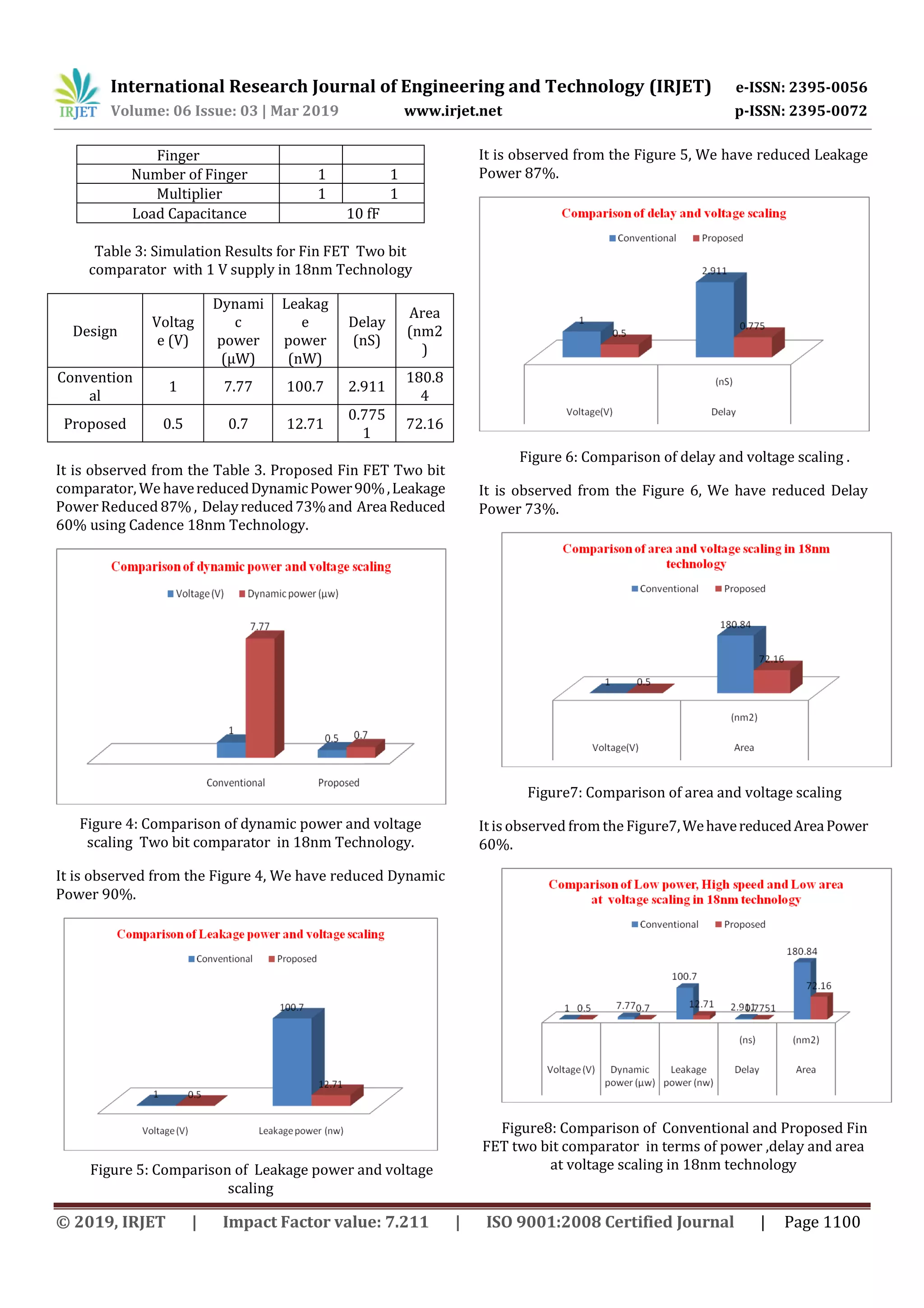
It is observed from the figure 8, Proposed Fin FET Two bit
comparator, We havereducedDynamicPower90%,Leakage
Power Reduced 87% , Delayreduced73%and AreaReduced
60% using Cadence 18nm Technology.
5. CONCLUSION
Two-bit magnitude comparator style victimization totally
different logic designs is planned during this temporary.
Comparison is most elementarymathematicaloperationthat
determines if one range is larger than, equal to, or but the
opposite range. Comparator is most elementary part that
performs comparison operation. This temporary presents
comparison between totally different logic designs wont to
style 2-Bit magnitude comparator. Comparison between
totally different styles is calculated by simulation that's
performed at 18nm technology in cadence EDA Tool. It is
observed from the Table 3, Proposed Fin FET Two Bit
Comparator,WehavereducedDynamicPower90%,Leakage
Power Reduced 87% , Delayreduced73%and AreaReduced
60% using Cadence 18nm Technology.
REFERENCES
[1] B. Keerthi Priya ; R. Manoj Kumar,"A new low power area
efficient 2bit magnitude comparator using modified GDI
technique in cadence 45nm technology", 2016 International
Conference on Advanced Communication Control and
Computing Technologies (ICACCCT),Year: 2016 Page s: 30 -
34,IEEE Conferences.
[2]. S. Kang and Y. Leblebici “CMOS Digital IntegratedCircuit,
Analysis and Design” (Tata McGraw-Hill, 3rd Ed, 2003).
[3]. A. Bellaouar and Mohamed I. Elmasry“LowPowerDigital
VLSI Design: Circuits and Systems” (Kluwer Academic
Publishers, 2nd Ed, 1995).
[4]. Anantha P. Chandrakasan and Robert W. Brodersen,
“Minimizing Power Consumption in CMOS circuits”.
Department of EECS, University of California at Barkeley,
http://bwrc.eecs.berkeley.edu/php/pubs/pubs.php/418/pa
per.fm.pdf, pp.1-64.
[5]. S. Salivahanan and S. Arivazhagan “Digital Circuits and
Design” (2nd Ed, 2004).
[6]. Dinesh Sharma, Microelectronics group, EE Department
IIT Bombay, “Logic Design”,
http://www.ee.iitb.ac.in/~smdp/DKStutorials/logic-
notes.pdf, pp.1-34.
[7]. N. Weste and K. Eshraghian “Principles of CMOS VLSI
Design: A system Perspective” (Addison- Wesley, 2nd Ed,
1993).
[8]. John P. Uyemura “Introduction to VLSI Circuit and
Systems”(JohnWileyIndia,ISBN:978-81-265-0915-7,2002).
[9]. R. Zimmermann and W. Fichtner, “Low Power Logic
Styles: CMOS Versus Pass Transistor Logic” IEEE Journal of
Solid State Circuits, Vol.32, No.7, pp1079-1090, July 1997.
[10] S. Cotofana, C. Lageweg, S. Vassilidis, “Addition Related
Arithmetic Operations via Controlled Transport of Charge”,
IEEE Trans. On Computers, Vol. 54(3), pp. 243-256, March
2005.
[11] ChirstophWasshuber, “SIMON – A simulator for single-
electron tunnel devices and circuits”, IEEE Trans. On
computer aided design of integrated circuits and systems,
Vol. 16(9), pp. 937-944, 1997.
[12] C. Wasshuber, H. Kosina,S.Selberherr,“Asingle-electron
device and circuit simulator”, Superlattices and
Microstructures, Vol. 21, pp. 37–42,
[13] Anbarasu Paulthurai, Balamurugan Dharmaraj “Single
Electron 2-Bit Multiplier”, International Journal of Computer
Applications Volume 42– No.4, March 2012
[14] Anjuli, Satyajit Anand “2-Bit Magnitude Comparator
Design Using Different Logic Styles”, International Journal of
Engineering Science Invention Volume 2 Issue 1 PP.13-24,
January. 2013](https://image.slidesharecdn.com/irjet-v6i3202-190816062038/75/IRJET-Fin-FET-Two-Bit-Comparator-for-Low-Voltage-Low-Power-High-Speed-and-Low-Area-in-18nm-Technology-5-2048.jpg)

This document presents a design for a 2-bit Fin FET comparator for low voltage, low power, high speed, and low area applications in 18nm technology. Simulation results show that the proposed Fin FET comparator reduces dynamic power by 90%, leakage power by 87%, delay by 73%, and area by 60% compared to a conventional design. The Fin FET comparator was designed and simulated using Cadence tools at a supply voltage of 0.5V in 18nm technology. Comparisons of the Fin FET and conventional designs show improvements in power, speed, and area with voltage scaling.


![[IJET-V1I2P6] Authors :Sarat K Kotamraju, K.Ch.Sri Kavya, A.Gnandeep Reddy, G...](https://cdn.slidesharecdn.com/ss_thumbnails/ijet-v1i2p6-150501052009-conversion-gate02-thumbnail.jpg?width=640&height=640&fit=bounds)