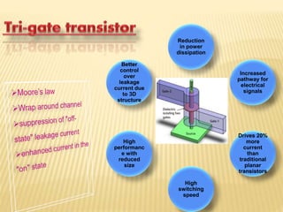
By 
Ruchira Shivsharan
Introduction 
Moore’s law 
Types of Multigate Transistor 
Planar double gate transistor 
FlexFET 
FinFET 
Tri-Gate transistor 
Gate all around FET 
3D transistor symbol and pin function 
Difference between planar and 3d transistor 
Key points 
3D tri-gate transistor benefits 
Fun Facts 
Application
Tri-Gate transistors, the first to be truly three-dimensional, mark a 
major revolution in the Semiconductor industry. The semiconductor 
industry continues to push technological innovation to keep pace 
with Moore’s Law, shrinking transistors so that ever more can be 
packed on a chip. However, at future technology nodes, the ability to 
shrink transistors becomes more and more problematic, in part due 
to worsening short channel effects and an increase in parasitic 
leakages with scaling of the gate-length dimension. In this regard Tri-gate 
transistor architecture makes it possible to continue Moore’s 
law at 22nm and below without a major transistor redesign. The 
physics, technology and the advantages of the device is briefly 
discussed in this paper.
“”THE NUMBER OF TRANSISTORS INCORPORATED IN 
A CHIP WILL APPROXIMATELY DOUBLE EVERY 24 
MONTHS.“ 
—GORDON 
MOORE
Planar double-gate transistor 
Flexfet 
FinFET 
Tri-gate transistor 
Gate-all-around (GAA) FET
Highly scalable due to its sub-lithographic channel length. 
Top gate MOSFET 
Bottom gate JFET 
The top and bottom gates provide transistor operation. 
The top gate operation affects the bottom gate operation and vice 
versa. 
 Flexfet was developed, and is manufactured, by American 
Semiconductor.
 Based on the earlier DELTA (single-gate) transistor 
design. 
 The conducting channel is wrapped by a thin silicon 
"fin”. 
 The thickness of the fin determines the effective 
channel length of the device. 
 The Wrap-around gate structure provides a better 
electrical control over the channel . 
 Helps in reducing the leakage current and 
overcoming other short channel effects.
The gate material surrounds the channel region on all sides. 
Gate-all-around FETs can have two or four effective gates. 
Gate-all-around FETs have been successfully built around 
a silicon nanowire. and etched InGaAs nanowires
Reduction 
in power 
dissipation 
Increased 
pathway for 
electrical 
signals 
Drives 20% 
more 
current 
than 
traditional 
planar 
transistors 
High 
switching 
speed 
Better 
control 
over 
leakage 
current due 
to 3D 
structure 
High 
performanc 
e with 
reduced 
size
Also called as multigate device or multiple gate 
field-effect transistor (MuGFET) refers to 
a MOSFET 
 incorporates more than one gate into a single 
device. The multiple gates may be controlled by a 
single gate electrode, 
in the multiple gate surfaces act electrically as a 
single gate, or by independent gate electrodes.
Key Points 
•Intel is introducing revolutionary Tri-Gate transistors on its 22 nm logic 
technology 
•Tri-Gate transistors provide an unprecedented combination of improved 
performance and energy efficiency 
•22 nm processors using Tri-Gate transistors, code-named Ivy Bridge, are now 
demonstrated working in systems 
•Intel is on track for 22 nm production in 2H ‘11, maintaining a 2-year cadence 
for introducing new technology generations 
•This technological breakthrough is the result of Intel’s highly coordinated 
research-development-manufacturing pipeline 
•Tri-Gate transistors are an important innovation needed to continue Moore’s 
Law
FUN FACTS: EXACTLY HOW SMALL (AND COOL) IS 22 
NANOMETERS? 
•The original transistor built by Bell Labs in 1947 was large enough that it was pieced 
together by hand. By contrast, more than 100 million 22nm tri-gate transistors could 
fit onto the head of a pin. 
•More than 6 million 22nm tri-gate transistors could fit in the period 
•A 22nm tri-gate transistor's gates that are so small, you could fit more than 4000 of 
them across the width of a human hair. 
•If a typical house shrunk as transistors have, you would not be able to see a house 
without a microscope. To see a 22nm feature with the naked eye, you would have to 
enlarge a chip to be larger than a house. 
•Compared to Intel's first microprocessor, the 4004, introduced in 1971, a 22nm CPU 
runs over 4000 times as fast and each transistor uses about 5000 times less energy. 
The price per transistor has dropped by a factor of about 50,000. 
•A 22nm transistor can switch on and off well over 100 billion times in one second. It 
would take you around 2000 years to flick a light switch on and off that many times.
The shorter the gate, the faster the computer can operate. While the 
new 3D transistors will have a gate length of 22 nanometers 
Computers implementing 3D silicon transistors will not only be able 
to run faster, but should also weigh less, and generate less heat than 
their present-day flat-transistor-using counterparts.
3d transistor
3d transistor
3d transistor

3d transistor

  • 1.
  • 2.
    Introduction Moore’s law Types of Multigate Transistor Planar double gate transistor FlexFET FinFET Tri-Gate transistor Gate all around FET 3D transistor symbol and pin function Difference between planar and 3d transistor Key points 3D tri-gate transistor benefits Fun Facts Application
  • 3.
    Tri-Gate transistors, thefirst to be truly three-dimensional, mark a major revolution in the Semiconductor industry. The semiconductor industry continues to push technological innovation to keep pace with Moore’s Law, shrinking transistors so that ever more can be packed on a chip. However, at future technology nodes, the ability to shrink transistors becomes more and more problematic, in part due to worsening short channel effects and an increase in parasitic leakages with scaling of the gate-length dimension. In this regard Tri-gate transistor architecture makes it possible to continue Moore’s law at 22nm and below without a major transistor redesign. The physics, technology and the advantages of the device is briefly discussed in this paper.
  • 4.
    “”THE NUMBER OFTRANSISTORS INCORPORATED IN A CHIP WILL APPROXIMATELY DOUBLE EVERY 24 MONTHS.“ —GORDON MOORE
  • 5.
    Planar double-gate transistor Flexfet FinFET Tri-gate transistor Gate-all-around (GAA) FET
  • 9.
    Highly scalable dueto its sub-lithographic channel length. Top gate MOSFET Bottom gate JFET The top and bottom gates provide transistor operation. The top gate operation affects the bottom gate operation and vice versa.  Flexfet was developed, and is manufactured, by American Semiconductor.
  • 10.
     Based onthe earlier DELTA (single-gate) transistor design.  The conducting channel is wrapped by a thin silicon "fin”.  The thickness of the fin determines the effective channel length of the device.  The Wrap-around gate structure provides a better electrical control over the channel .  Helps in reducing the leakage current and overcoming other short channel effects.
  • 11.
    The gate materialsurrounds the channel region on all sides. Gate-all-around FETs can have two or four effective gates. Gate-all-around FETs have been successfully built around a silicon nanowire. and etched InGaAs nanowires
  • 12.
    Reduction in power dissipation Increased pathway for electrical signals Drives 20% more current than traditional planar transistors High switching speed Better control over leakage current due to 3D structure High performanc e with reduced size
  • 13.
    Also called asmultigate device or multiple gate field-effect transistor (MuGFET) refers to a MOSFET  incorporates more than one gate into a single device. The multiple gates may be controlled by a single gate electrode, in the multiple gate surfaces act electrically as a single gate, or by independent gate electrodes.
  • 20.
    Key Points •Intelis introducing revolutionary Tri-Gate transistors on its 22 nm logic technology •Tri-Gate transistors provide an unprecedented combination of improved performance and energy efficiency •22 nm processors using Tri-Gate transistors, code-named Ivy Bridge, are now demonstrated working in systems •Intel is on track for 22 nm production in 2H ‘11, maintaining a 2-year cadence for introducing new technology generations •This technological breakthrough is the result of Intel’s highly coordinated research-development-manufacturing pipeline •Tri-Gate transistors are an important innovation needed to continue Moore’s Law
  • 22.
    FUN FACTS: EXACTLYHOW SMALL (AND COOL) IS 22 NANOMETERS? •The original transistor built by Bell Labs in 1947 was large enough that it was pieced together by hand. By contrast, more than 100 million 22nm tri-gate transistors could fit onto the head of a pin. •More than 6 million 22nm tri-gate transistors could fit in the period •A 22nm tri-gate transistor's gates that are so small, you could fit more than 4000 of them across the width of a human hair. •If a typical house shrunk as transistors have, you would not be able to see a house without a microscope. To see a 22nm feature with the naked eye, you would have to enlarge a chip to be larger than a house. •Compared to Intel's first microprocessor, the 4004, introduced in 1971, a 22nm CPU runs over 4000 times as fast and each transistor uses about 5000 times less energy. The price per transistor has dropped by a factor of about 50,000. •A 22nm transistor can switch on and off well over 100 billion times in one second. It would take you around 2000 years to flick a light switch on and off that many times.
  • 23.
    The shorter thegate, the faster the computer can operate. While the new 3D transistors will have a gate length of 22 nanometers Computers implementing 3D silicon transistors will not only be able to run faster, but should also weigh less, and generate less heat than their present-day flat-transistor-using counterparts.