This document analyzes the analog and RF behaviors of junctionless double-gate vertical MOSFETs (n-jldgvm) compared to traditional junction double-gate vertical MOSFETs (n-jdgvm). It demonstrates that the n-jldgvm device shows a 4% increase in transconductance and improved cut-off frequency (3.4%) and gain-bandwidth product (7%) over the n-jdgvm device, indicating better performance for high-frequency applications. The paper highlights the advantages of junctionless transistors in simplifying the fabrication process while providing enhanced electrical characteristics.
![Bulletin of Electrical Engineering and Informatics
Vol. 9, No. 1, February 2020,pp. 101~108
ISSN: 2302-9285,DOI: 10.11591/eei.v9i1.1861 101
Journal homepage: http://beei.org
Analysis of analog and RF behaviors in junctionless double gate
vertical MOSFET
K. E. Kaharudin, Z. A. F. M. Napiah, F. Salehuddin, A. S. M. Zain, Ameer F. Roslan
MiNE, Centre for Telecommunication Research and Innovation, Faculty of Electronics and Computer Engineering,
Universiti Teknikal Malaysia Melaka (UTeM), Hang Tuah Jaya, Durian Tunggal, 76100 Melaka
Article Info ABSTRACT
Article history:
Received Aug 10, 2019
Revised Oct 22, 2019
Accepted Dec 1, 2019
The prime obstacle in continuing the transistor’s scaling is to maintain
ultra-shallow source/drain (S/D) junctions with high doping concentration
gradient, which definitely demands an advanced and complicated S/D and
channel engineering. Junctionless transistor configuration has been found to
be an alternative device structure in which the junction and doping gradients
could be totally eliminated, thus simplifying the fabrication process.
In this paper, a process simulation has been performed to study the impact of
junctionless configuration on the analog and RF behaviors of double-gate
vertical MOSFET. The result proves that the performance of n-channel
junctionless double-gate vertical MOSFET (n-JLDGVM) is slightly better
than the junction double-gate vertical MOSFET (n-JDGVM). Junctionless
device exhibits better analog behaviors as the transconductance (gm)
is increased by approximately 4%. In term of RF behaviors, the junctionless
device exhibits 3.4% and 7% higher cut-off frequency (fT) and gain
band-width product (GBW) respectively over the junction device.
Keywords:
Cut-off frequency
Drain conductance
Gain band-width product
Intrinsic gate delay
Transconductance
This is an open access article under the CC BY-SA license.
Corresponding Author:
F. Salehuddin,
Centre for Telecommunication Research and Innovation,
Faculty of Electronics and ComputerEngineering,
Universiti TeknikalMalaysia Melaka (UTeM),
HangTuah Jaya,Durian Tunggal, 76100 Melaka.
Email: fauziyah@utem.edu.my
1. INTRODUCTION
The utilization of low power and high frequency based devices are very crucial for future electronic
applications. Miniaturization in transistor’s size with improvement in analog and RF performances is a vital
goal of the microelectronics community. For realizing this goal, a number of device engineering methods
such as source/drain engineering, multi-gate technology, dual material gate (DMG) technology, channel
engineering, gate stack (GS) engineering and junctionless configuration have been carried out for
decades [1–8]. According to International Technology Roadmap for Semiconductors 2013 (ITRS 2013)
report [9], a precisely controlled process flow for the fabrication of transistors is becoming extremely
complicated for deep sub-micron devices. As the transistor’s size shrinks drastically towards sub-nanometer
regime, the threshold voltage (VTH) would be rolled-off along with the decreasing channel length (Lch),
which eventually deteriorating the overall performance due to short channel effects (SCE) [10]. Th e most
difficult challenge in transistor’s miniaturization is to form ultra -shallow source/drain (S/D) junctions with
high doping gradient which requires advanced source/drain and channel engineering processes [11, 12].
For that reason, a lot of alternative device structures have emerged for realizing the Moore’s law prediction
without degrading the transistor performances.](https://image.slidesharecdn.com/13-1861-210727023737/75/Analysis-of-analog-and-RF-behaviors-in-junctionless-double-gate-vertical-MOSFET-1-2048.jpg)
![ ISSN: 2302-9285
Bulletin of Electr Eng & Inf, Vol. 9, No. 1, February 2020 : 101 – 108
102
Recently, the junctionless transistor configuration has received a lot of attention in producing
the ultra-small, low power and high frequency transistor due to its simplified fabrication
process [6, 8, 13–16]. Instead of having the intricate source/drain and channel engineering processes,
the junctions of the transistor can be completely removed by doping the source/drain and channel regions
with similar polarity dopant, either n-type (for n-channel transistor) or p-type (for p-channel transistor)
dopant.The junctionless-mode configuration could avoid the adversity of forming the intricate junctions with
high doping gradient, especially for short channel devices. The analog and RF behaviors in junctionless
transistors are very important to be properly investigated, especially for system on chip (SoC) and system in
package (SiP) applications [11, 17–19]. Thus, this paper emphasizes on the performance analysis of analog
and RF behaviors of n-channel junctionless double-gate vertical MOSFET (JLDGVM) and n-channel
junction double-gate vertical MOSFET (JDGVM). The presented work in this paper is organized as follows:
Section 2 briefly describes the device simulation of both JLDGVM and JDGVM and the process flow using
Silvaco simulator. Section 3 discusses the comparative analysis of the analog and RF behaviors between
n-JLDGVM and n-JDGVM in term of transconductance (gm), transconductance generation factor (TGF),
output conductance (gd), early voltage (VEA), gate-to-source capacitance (Cgs), gate-to-drain (Cgd),
parasitic capacitance (Cgg), intrinsic gate delay (τint), cut-off frequency (FT) and
Gain Band-Width product (GBW). Finally, the conclusions and future work are presented in section 4.
2. DEVICE SIMULATION
The devices are designed based on high-k material (hafnium dioxide) as gate stack and extensive
investigation is conducted by taking junctionless and junction configuration to verif y the effects on various
analog and RF behaviors. The distinctive different between junctionless and junction configuration of
double-gate vertical MOSFET is their opposite channel type as depicted in Figure 1. The channel region for
n-JLDGVM is heavily doped with the similar polarity as source/drain doping in order to form N- N+- N type.
In contrast, the channel region for n-JDGVM is doped with the opposite polarity as source/drain doping
to form N-P-N type.
(a) (b)
Figure 1. 2D structure of n-channeldouble-gate vertical MOSFETs, (a) Junctionless (n-JLDGVM),
(b) Junction (n-JDGVM)
Extensive device simulation is performed via Silvaco Atlas for extracting the DC and AC
characteristics of n-JLDGVM and JDGVM devices. The device simulation is conducted based on the current
continuity and drift diffusion models in order to compute the current-voltage characteristics. Besides that,
the mobility model is also included for considering the scattering processes such as lattice vibration
(phonons), impurity ions, surfaces,and other materialimperfections. The impact of these scattering processes
would lead to low carrier mobility since they involve in both current continuity and drift -diffusion
models [20]. For this case, the LombardiCVT model is opted to be employed to perform accurate simulation
of non-planarMOSFET like JLDGVM and JDGVM devices.
3. RESULTS AND DISCUSSION
In this section, the simulation results and discussion are critically described for both n-JLDGVM
and n-JDGVM devices. For the purpose of performance analysis of analog and RF behaviors in JLDGVM](https://image.slidesharecdn.com/13-1861-210727023737/75/Analysis-of-analog-and-RF-behaviors-in-junctionless-double-gate-vertical-MOSFET-2-2048.jpg)
![Bulletin of Electr Eng & Inf ISSN: 2302-9285
Analysis of analog and RF behaviors in junctionless double gate vertical MOSFET (K. E. Kaharudin)
103
and JDGVM devices, the VTH values of both devices were fixed at 0.2 V. The other DC characteristics
are normalized to the fixed VTH value for unbiased performance evaluation. The DC analysis is an initial
step for the further evaluation of analog and RF behaviors in both devices. The analog and RF behaviors
for both devices are discussed in the following sub-sections.
3.1. Analog behaviors
Analog behaviors such as transconductance (gm), transconductance generation factor (TGF), drain
conductance (gd) and early voltage (VEA) are presented and discussed here for analog performance point
of view. The transconductance (gm) is an important figure of merit that implies how effective a transistor
converts a voltage to a current. It is mainly employed for measuring the amplifier’s gain. On the other hand,
the transconductance generation factor (TGF) is also a significant figure of merit that implies how efficient
a transistor converts DC power into AC frequency and gain. Figures 2 and 3 present the plot for gm and TGF
respectively as a function of gate voltage (VG). The n-JLDGVM device demonstrates approximately 4%
higher tranconductance (gm) than the JDGVM device. Below the gate voltage (VG) of ~ 0.6V, the gm for
both devices linearly increases as the VG increases. After VG ~ 0.6V, the gm for both devices begins to
saturate until its reach maximum gate bias. It is observed that the maximum gm at VG=1 V for n-JLDGVM
device is approximately 4% higher than the n-JDGVM device. Due to bulk phenomenon in junctionless
configuration, the gm is slightly increased as it is approaching the maximum gate voltage. The improved gm
value in junctionless configuration agreed with previous works conducted [16]. A higher gm of
the n-JLDGVM device indicates that the conducting channel possesses higher transport efficiency which
is suitable for analog based applications. In term of TGF, the n-JLDGVM device demonstrates
approximately 20% higher TGF compared to JDGVM device. The slight improvement in TGF is in
agreement with the results obtained by previous researchers [21, 22]. The gm/ID ratio is mainly influenced
by the pillar/body factor of the devices in weak inversion region. However, the gm/ID ratio for
n-JDGVM is observed to be slightly decreased due to strong inversion in the channel region that causes
a decrease in electron mobility at higher doping concentration.
Figure 2. Transconductance (gm)as a function
of gate voltage
Figure 3. TGF as a function of gate voltage
The drain conductance (gd) is also an important analog characteristic that decides a transistor’s
performance in analog based applications. The ultrathin pillar feature in both n-JLDGVM and n-JDGVM
devices are very crucial in forming a fully depleted channel that could reduce the impact ionization effects.
The impact ionization effects such as kink effect and parasitic bipolar action, normally experienced in most
of bulk transistors would subsequently lead to a much higher gd. The value of gd is very crucia l in
determining the drain current (ID) to drain conductance (gd) ratio, also called as early voltage (VEA).
The VEA is not a constant value, but depends upon the channel length, inversion level and also the drain
voltage (VD). Figures 4 and 5 show the plot of drain conductance (gd) and the early voltage (VEA)
respectively at VG=0.5V as a function of VD. The n-JLDGVM device carries higher drain current and thus
results in higher drain conductance than the n-JDGVM device.](https://image.slidesharecdn.com/13-1861-210727023737/75/Analysis-of-analog-and-RF-behaviors-in-junctionless-double-gate-vertical-MOSFET-3-2048.jpg)
![ ISSN: 2302-9285
Bulletin of Electr Eng & Inf, Vol. 9, No. 1, February 2020 : 101 – 108
104
Figure 4. Drain conductance (gd) asa function
of drain voltage
Figure 5. Early voltage (VEA) as a function
of drain voltage
The n-JLDGVM device exhibits approximately 11% higher gd than n-JDGVM device. In most
cases, the gd magnitude is strongly influenced by channel length modulation. In practical, CMOS analog
circuits preferably need MOSFETs that exhibit low gd magnitude for attaining much higher gain. A slight
improvement (0.5%) in VEA can be observed in case of n-JLDGVM device as compared to n-JDGVM,
mainly due to short channel effects (SCE) suppression. The side gates have better control over the charge
carriers in the junctionless mode which slightly mitigating the SCE. As a result, the value of early voltage in
n-JLDGVM device slightly increases and the dependence of the drain current on the drain voltage
is minimized. Evidence of improved VEA for junctionless configura tion is also reported by [11, 16].
The intrinsic gain (AV) is another important figure of merit for benchmarking the analog performance of
operationaltransconductance amplifiers. The AV for the devices can be calculated as:
EA
D
m
d
m
V V
I
g
g
g
A
=
=
The extracted and computed values of gm, TGF, gd, VEA and AV for n-JLDGVM and n-JDGVM
devices are summarized in Table 1. It is observed that the n-JLDGVM device exhibits marginally 2% higher
AV than n-JDGVM device. Higher AV is pretty much desired in analog designs because it implies how
efficient a transistor could amplify the input signal when it is biased to operate in both active and saturation
region of operation.
Table 1. Analog performances forJLDGVM and JDGVM
Device gm (mS/µm) TGF (V-1
) gd (mS/µm) VEA (V) AV (dB)
JLDGVM 2.39 267 0.772 0.596 9.8
JDGVM 2.30 214 0.761 0.593 9.6
3.2. RF behaviors
Several crucial RF behaviors of the device are extracted and computed. Initially, the extractions of
Cgs and Cgd are carried out through small signal analysis after post-processing DC analysis. The values of
capacitance between source and drain regions are measured by supplying a single AC frequency (f) of 1 MHz
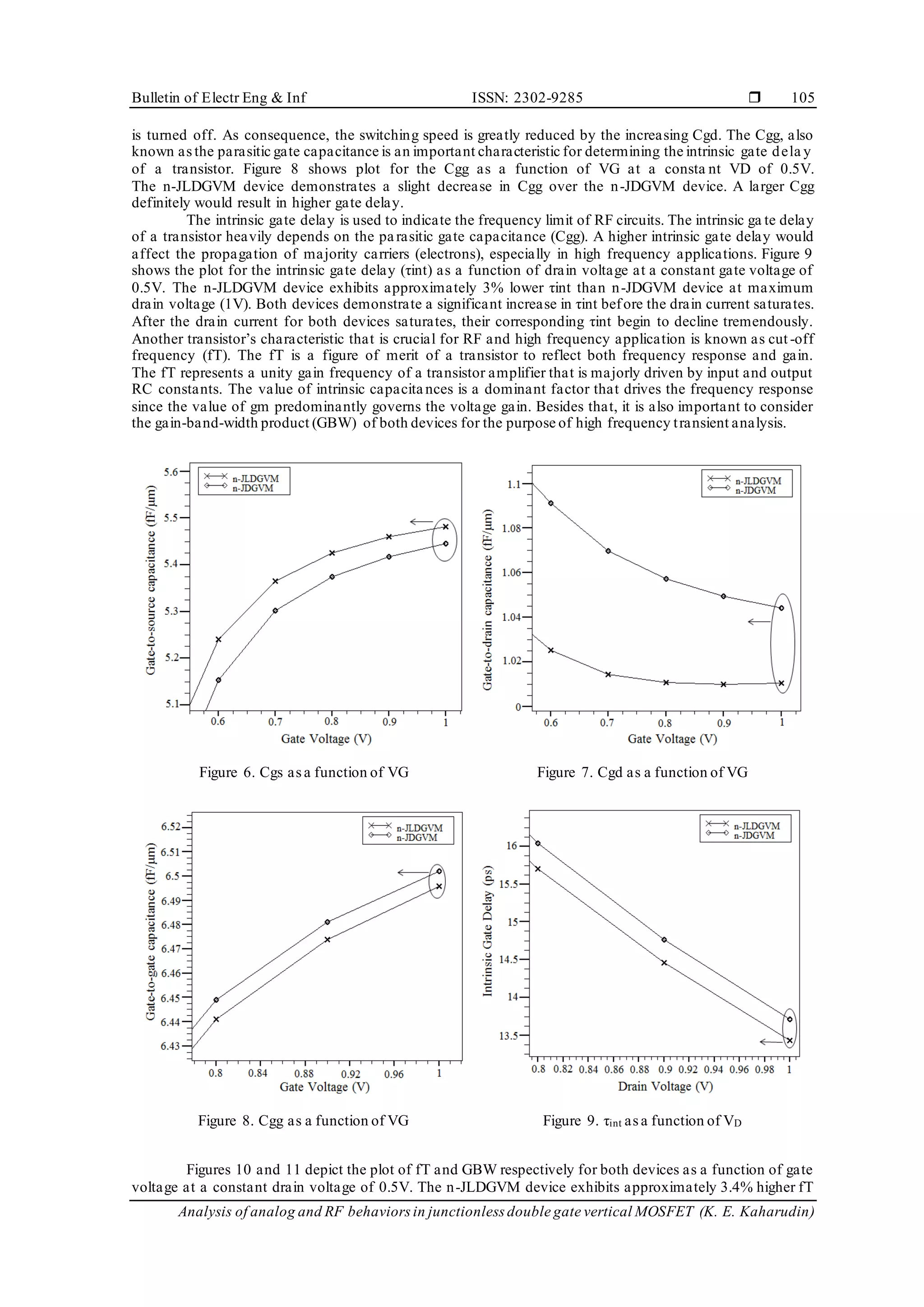
as the VG is swept from 0 V to 1 V with a step of 0.01 V. Figures 6 and 7 depict the plot of intrinsic
capacitances (Cgs and Cgd) respectively as a function of VG at a fixed VD of 0.5 V. Based on the combined
plot, the Cgs for n-JLDGVM device is observed to be approximately 3% higher than the n-JDGVM device.
Furthermore, both devices show an almost linear increase in Cgs value as the gate voltage is shifted towards
its maximum value (1 V). The difference of Cgs for both devices is less prominent as it does not contribute
significant changes in output current when the gate is turned off and the time required for the output to turn
off completely. On the other hand, the n-JLDGVM device exhibits approximately 3% lower Cgd compared
to n-JDGVM device. Both devices exhibit an almost constant Cgd value as the gate voltage is shifted towards
its maximum value (1V). The high Cgd is not desirable in RF and high frequency applications because
it would delay the rise in drain current after the gate is turn on and the fall in drain current after the gate](https://image.slidesharecdn.com/13-1861-210727023737/75/Analysis-of-analog-and-RF-behaviors-in-junctionless-double-gate-vertical-MOSFET-4-2048.jpg)
![ ISSN: 2302-9285
Bulletin of Electr Eng & Inf, Vol. 9, No. 1, February 2020 : 101 – 108
106
compared to n-JDGVM device. The slight improvement in fT for n-JLDGVM device over the n-JDGVM
device is due to junctionless configuration which alters the energy band structure of the conductive layer.
As a result, the effective mass of electrons is slightly reduced, thus increasing its mobility. The variation of
fT over the increasing gate voltage is mainly affected by the gm and the intrinsic capacitances. Hence, high
gm and low intrinsic capacitances are significantly required in achieving better cut-off frequency (fT) for
high speed RF applications. In term of GBW, the n-JLDGVM device shows 7% higher GBW than
the n-JDGVM device. The minor improvement in GBW of n-JLDGVM device is mainly influenced by its
higher gm and the lower Cgd than the n-JDGVM device. The high GBW is very desirable for circuit
applications that require extremely high speed and low input bias current such as RF amplifiers [23].
The extracted and computed values of Cgs, Cgd, Cgg, τint, FT and GBW for n-JLDGVM and n-JDGVM
devices are summarized in Table 2. Based on the obtained results, it can be concluded that the junctionless
configuration does improve the overall device characteristics of double-gate vertical MOSFET, including
the analog and RF behaviors. A slight improvement in ID, gm, TGF, gd, VEA, AV, Cgs, Cgd Cgg, τint, fT
and GBW clearly indicate that the n-JLDGVM device can be a potential transistor configuration for future
low power and high frequency analog and RF applications. However, the analog and RF behaviors for
the n-JLDGVM device still could be further improved by optimizing the geometrical and process parameters.
Thus, various optimization methods [24–30] could be applied to further enhance the DC and AC
characteristics for analogand RF applications.
Figure 10. fT as a function of VG Figure 11. GBW as a function of VG
Table 2. RF performances forJLDGVM and JDGVM
Device Cgs (fF/µm) Cgd (fF/µm) Cgg (fF/µm) τint (ps) fT (GHz) GBW (GHz)
JLDGVM 5.48 1.01 6.49 13.4 59 377
JDGVM 5.45 1.04 6.50 13.7 57 351
4. CONCLUSION
In summary, the DC, analog and RF behaviors of n-channel junctionless double-gate vertical
MOSFET (n-JLDGVM) are investigated and compared with the n-channel junction double-gate vertical
MOSFET (n-JDGVM). The device performance between n-JLDGVM and n-JDGVM are compared in term
of gm, TGF, gd, VEA, AV, Cgs, Cgd Cgg, τint, fT and GBW. The results show that the junctionless device
demonstrates slightly better analog behaviors over the junction device as the gm magnitude is increased
by 4%. In term of RF behaviors, the junctionless device exhibits 3.4% and 7% higher fT and GBW
respectively over the junction device. These show that n-JLDGVM device can be a potential transistor
configuration for future low power and high frequency analogand RF applications. Furthermore, both analog
and RF behaviors of the n-JLDGVM device could be possibly improved by optimizing geometrical and
process parametersthrough statistical methods or predictive analysis.
ACKNOWLEDGEMENTS
The authors would like to thank to the Ministry of Higher Education (MOHE) of Malaysia,
Mybrain15 and Centre for Telecommunication Research and Innovation (CeTRI),Faculty of Electronics a nd](https://image.slidesharecdn.com/13-1861-210727023737/75/Analysis-of-analog-and-RF-behaviors-in-junctionless-double-gate-vertical-MOSFET-6-2048.jpg)
![Bulletin of Electr Eng & Inf ISSN: 2302-9285
Analysis of analog and RF behaviors in junctionless double gate vertical MOSFET (K. E. Kaharudin)
107
Computer Engineering (FKEKK), Universiti Teknikal Malaysia Melaka (UTeM) for sponsoring this research
study under research grant PJP/2018/FKEKK(2B)/S01614).
REFERENCES
[1] J. Dubois, M. Bolt, P. Semiconductors, and H. Tuinhout, “Impact of source/drain implants on threshold voltage
matching in deep sub-micron CMOS technologies,” in European Solid-State Device Research Conference,
pp. 115–118, 2002.
[2] S. K. Mohapatra, K. P. Pradhan, L. Artola, and P. K. Sahu, “Estimation of analog/RF figures-of-merit using device
design engineering in gate stack double gate MOSFET,” Materials Science in Semiconductor Processing, vol. 31,
pp. 455–462, 2015.
[3] S. Archana, G. Vallathan, and M. A. Kumar, “Analytical modeling of dual material junctionless surrounding gate
MOSFET,” SSRG International Journal of Electronics and Communication Engineering, vol. 4, no. 3, pp. 40–43,
2017.
[4] Q. Xu et al., “Ion-implanted TiN metal gate with dual band-edge work function and excellent reliability for
advanced CMOS device applications,” in IEEE Transactions on Electron Devices, vol. 62, no. 12, pp. 4199-4205,
Dec 2015.
[5] A. Kumar, M. M. Tripathi, and R. Chaujar, “Comprehensive analysis of sub-20 nm black phosphorus based
junctionless-recessed channel MOSFET for analog/RF applications,” Superlattices and Microstructures, vol. 116,
no. February, pp. 171–180, 2018.
[6] N. F. Kosmani, F. A. Hamid, and M. A. Razali, “A comparison of performance between double-gate and
gate-all-around nanowire MOSFET,” Indonesian Journal of Electrical Engineering and Computer Science, vol. 13,
no. 2, pp. 801–807, 2019.
[7] M. Khaouani and A. Guen-bouazza, “Impact of multiple channels on the characteristics of rectangular GAA
MOSFET,” International Journal of Electrical and Computer Engineering, vol. 7, no. 4, pp. 1899–1905, 2017.
[8] M. A. Riyadi, I. D. Sukawati, T. Prakoso, and Darjat, “Influence of gate material and process on junctionless FET
subthreshold performance,” International Journal of Electrical and Computer Engineering, vol. 6, no. 2,
pp. 895–900, 2016.
[9] ITRS, “International Technology Roadmap Semiconductor,” 2013.
[10] A. F. Roslan, F. Salehuddin, A. S. M. Zain, K. E. Kaharudin, I. Ahmad, and H. Hazura, “Comparative high-k
material gate spacer impact in DG-FinFET parameter variations between two structures,” Indonesian Journal of
Electrical Engineering and Computer Science, vol. 14, no. 2, pp. 573–580, 2019.
[11] Y. Chen, M. Mohamed, M. Jo, U. Ravaioli, and R. Xu, “Junctionless MOSFETs with laterally graded-doping
channel for analog/RF applications,” Journal of Computational Electronics, vol. 12, no. 4, pp. 757–764, 2013.
[12] A. F. Roslan, F. Salehuddin, A. S. M. Zain, K. E. Kaharudin, H. Hazura, and A. R. Hanim, “30 nm DG-FinFET 3D
construction impact towards short channel effects,” Indonesian Journal of Electrical Engineering and Computer
Science, vol. 12, no. 3, pp. 1358–1365, 2018.
[13] C. W. Lee, I. Ferain, A. Afzalian, R. Yan, N. D. Akhavan, P. Razavi, and J. P. Colinge, “Performance estimation of
junctionless multigate transistors,” Solid-State Electronics, vol. 54, no. 2, pp. 97–103, 2010.
[14] J. P. Colinge, C. W. Lee, I. Ferain, N. D. Akhavan, R. Yan, P. Razavi, R. Yu, A. N. Nazarov, and R. T. Doria,
“Reduced electric field in junctionless transistors,” Applied Physics Letters, vol. 96, no. 7, pp. 073510-1- 073510-3,
2010.
[15] J. P. Colinge, C. W. Lee, A. Afzalian, N. D. Akhavan, R. Yan, I. Ferain, P. Razavi, B. O’Neill, A. Blake, M. White,
A. M. Kelleher, B. McCarthy, and R. Murphy, “Nanowire transistors without junctions,” Nature Nanotechnology,
vol. 5, no. 3, pp. 225–229, 2010.
[16] R. T. Doria et al., "Junctionless multiple-gate transistors for analog applications," in IEEE Transactions on
Electron Devices, vol. 58, no. 8, pp. 2511-2519, Aug 2011.
[17] P. K. Sahu, S. K. Mohapatra, and K. P. Pradhan, “Impact of downscaling on analog/RF performance of
sub-100nm GS-DG MOSFET,” Journal of Microelectronics, Electronic Components and Materials, vol. 44, no. 2,
pp. 119–125, 2014.
[18] B. Lakshmi and R. Srinivasan, “Effect of process parameter variation on ft in coventional and junctionless
gate-all-around devices,” Journal of Engineering Science and Technology, vol. 10, no. 8, pp. 994–1008, 2015.
[19] F. Salehuddin, K. E. Kaharudin, A. S. M. Zain, A. K. M. Yamin, and I. Ahmad, “Analysis of process parameter
effect on DIBL in n-channel MOSFET device using L27 orthogonal array,” in International Conferences on
Fundamental and Applied Sciences, AIP Conf. Proc., vol. 1621, no. 1, pp. 322–328, 2014.
[20] Silvaco, “Silvaco ATLAS manual Device Simulation Software,” 2006.
[21] R. K. Baruah and R. P. Paily, “Analog performance of bulk planar junctionless transistor (BPJLT),” in Computing
Communication & Networking Technologies (ICCCNT), Third International Conference, pp. 1–4, 2012.
[22] J. P. Colinge, A. Kranti, R. Yan, I. Ferain, D. Akhavan, P. Razavi, C. W. Lee, R. Yu, and C. A. Colinge,
“A Simulation Comparison between junctionless and inversion-mode MuGFETs.,” ECS Transactions, vol. 35,
no. 5, pp. 63–73, 2011.
[23] S. Singh and P. Kumar, “Transient analysis & performance estimation of gate inside junctionless transistor
(GI-JLT),” International Journal of Nuclear and Quantum Engineering, vol. 8, no. 10, pp. 1641–1645, 2014.
[24] K. E. Kaharudin, F. Salehuddin, A. S. M. Zain, and M. N. I. A. Aziz, “Comparison of Taguchi method and central
composite design for optimizing process parameters in vertical double gate MOSFET,” ARPN Journal of
Engineering and Applied Sciences, vol. 12, no. 19, pp. 5578–5590, 2017.
[25] K. E. Kaharudin, F. Salehuddin, A. S. M. Zain, and M. N. I. A. Aziz, “Impact of different dose, energy and tilt
angle in source/drain implantation for vertical double gate PMOS device,” Journal of Telecommunication,
Electronic and Computer Engineering, vol. 8, no. 5, pp. 23–28, 2016.](https://image.slidesharecdn.com/13-1861-210727023737/75/Analysis-of-analog-and-RF-behaviors-in-junctionless-double-gate-vertical-MOSFET-7-2048.jpg)
![ ISSN: 2302-9285
Bulletin of Electr Eng & Inf, Vol. 9, No. 1, February 2020 : 101 – 108
108
[26] K. E. Kaharudin, A. H. Hamidon, and F. Salehuddin, “Implementation of Taguchi modeling for higher drive
current (ION) in vertical DG-MOSFET device,” Journal of Telecommunication, Electronic and Computer
Engineering, vol. 6, no. 2, pp. 11–18, 2014.
[27] K. E. Kaharudin, F. Salehuddin, A. S. Zain, and M. N. I. Aziz, “Application of Taguchi-based grey fuzzy logic for
simultaneous optimization in TiO2/WSix-based vertical double-gate MOSFET,” Journal of Telecommunication,
Electronic and Computer Engineering, vol. 9, no. 2–13, pp. 23–28, 2017.
[28] K. E. Kaharudin, F. Salehuddin, and A. S. M. Zain, “Optimization of electrical properties in TiO2/WSix-based
vertical DG-MOSFET using Taguchi-based GRA with ANN,” Journal of Telecommunication, Electronic and
Computer Engineering, vol. 10, no. 1, pp. 69–76, 2018.
[29] R. Norani, “A dynamic simulation on single gate junctionless field effect transistor based on genetic algorithm,”
Advances in Computer Science: an International Journal, vol. 3, no. 5, pp. 140–145, 2014.
[30] K. E. Kaharudin, F. Salehuddin, A. S. M. Zain, and M. N. I. A. Aziz, “Influence of halo and source/drain implant
variations on the drive current in p-channel vertical double gate MOSFET,” in Proceedings of Mechanical
Engineering Research Day, pp. 33–34, 2016.
BIOGRAPHIES OF AUTHORS
K. E. Kaharudin received Ph.D in Electronic Engineering and M. Eng degree in Computer
Engineering from Technical University of Malaysia Melaka (UTeM), in 2017 and 2013
respectively. His Ph.D project focused on the process optimization of vertical double gate
MOSFET. His research’s interests include CMOS design, microelectronics, semiconductors,
engineering optimization and artificial intelligence. Recently, his efforts emphasize on
the simulation design of Junctionless MOSFET, silicon-on-insulator (SOI) MOSFET,
high-k/metal-gate stack technology and design of experiment (DoE).
Z. A. F. M. Napiah received the B.Eng. degree in electrical engineering and the M.Eng. degree
in Microelectronic from Universiti Teknologi Malaysia (UTM). He received the Ph.D. degree in
Microelectronics from Kanawa University, Japan. He is currently a senior lecturer at Faculty of
Electronic and Computer Engineering (FKEKK), UTeM. His research interest includes process
and device simulation of MOSFET device, advanced CMOS design and CMOS based
Photodetector and Photoreceiver
F. Salehuddin received the B.Eng. degree in electrical engineering (Communication) from
Universiti Teknologi Mara (UiTM), Malaysia in 2001 and the M.Sc. degree in Electrical,
Electronic and System Engineering from Universiti Kebangsaan Malaysia, in 2003. She received
the Ph.D. degree in Microelectronics Engineering from Universiti Tenaga Nasional (UNITEN),
Malaysia in 2012. She joined Universiti Teknikal Malaysia Melaka (UTeM) in December 2001
as a tutor and is currently a senior lecturer at Faculty of Electronic and Computer Engineering
(FKEKK), UTeM. Her research interest includes process and device simulation of nanoscale
MOSFETs device, advanced CMOS design, optimization approach (DOE) and process
parameter variability.
A. S. M. Zain received the B.Eng degree in electrical, Electronic and System engineering and M.
Sc in Microelectronics from National University of Malaysia (UKM), Malaysia She received
the Ph.D. degree in Nanoelectronics Engineering from University of Glasgow, UK in 2013.
She is currently working as a senior lecturer at Faculty of Electronic and Computer Engineering
(FKEKK), Universiti Teknikal Malaysia Melaka (UTeM). Her research interest includes
Nanoscale Device Design and Simulation, Variability and Reliability of Emerging Technology
Devices, IC Design for Biomedical Applications.
Ameer F. Roslan received by. Sc. Degree in Telecommunication Engineering from Technical
University of Malaysia Melaka (UTeM), in 2017. He is currently pursuing his M.Sc degree in
electronics and doing research on the DG-FinFET device at Centre for Telecommunication
Research and Innovation, Faculty of Electronics and Computer Engineering, Technical
University of Malaysia Melaka (UTeM). His research interest includes the DG-FinFET
architecture and statistical](https://image.slidesharecdn.com/13-1861-210727023737/75/Analysis-of-analog-and-RF-behaviors-in-junctionless-double-gate-vertical-MOSFET-8-2048.jpg)