This document reviews the development of interconnect technology in integrated circuits from aluminum to copper and low-k dielectrics. It discusses how copper replaced aluminum as the interconnect material due to its higher conductivity and electromigration resistance. Copper is patterned using the damascene process where it is deposited into trenches etched into a dielectric. As feature sizes shrank below 180nm, the dielectric constant of the interlayer dielectric (ILD) needed to be reduced to prevent delays, leading to the use of low-k materials like carbon-doped oxides and porous oxides with dielectric constants as low as 2.1.
1) Rectangular waveguides can transmit electromagnetic waves above a certain cutoff frequency, acting as a high-pass filter. They support transverse electric (TE) and transverse magnetic (TM) modes of propagation.
2) For TM modes, the electric field is transverse to the direction of propagation, while the magnetic field has a longitudinal component. The modes are denoted TMmn, with m and n indicating the number of half-wavelength variations across the width and height.
3) For TE modes, the magnetic field is entirely transverse, while the electric field has a longitudinal component. These modes are denoted TEmn, with m and n having the same meaning as in the TM case.
Here are the all short channel effects that you require.It consist of:-
Drain Induced Barrier Lowering
Hot electron Effect
Impact Ionization
Surface Scattering
Velocity saturation
This document is the preface to a book about silicon carbide power devices. It provides background on the development of power semiconductor devices, including bipolar transistors, thyristors, power MOSFETs, and IGBTs. It discusses the author's 1979 proposals to develop MOS-bipolar devices and power devices using wide bandgap semiconductors like silicon carbide and gallium arsenide. The preface describes early research efforts to develop GaAs and SiC power devices and outlines the chapters in the book, which provide analysis and modeling of various SiC power device structures like Schottky rectifiers, JFETs, MOSFETs, and their advantages over silicon devices.
The document discusses the different modes of operation of a MOS capacitor:
1. Flat band mode occurs when no potential is applied and the energy bands are flat.
2. Accumulation mode occurs when a negative charge is applied to a p-type semiconductor, accumulating a negative charge at the oxide interface.
3. Depletion mode occurs when a positive gate voltage is applied, depleting the p-type semiconductor of its positive charge carriers.
4. Inversion mode occurs at higher positive voltages when the depletion of positive charge leads to an accumulation of negative charge, inverting the type of charge carriers at the interface.
First op amps built in 1930’s-1940’s
Technically feedback amplifiers due to only having one useable input
Used in WW-II to help how to strike military targets
Buffers, summers, differentiators, inverters
Took ±300V to ± 100V to power
This document outlines the syllabus and content for a basic electronics course. It discusses that the course grade will be based on midterm, final, and sessional marks. Sessional marks depend on behavior, participation, assignments, presentations, attendance, and quizzes. Contact information for the instructor is provided. Recommended reference materials are listed. An introduction to electronics and its role in daily life is given. The history of electronics from vacuum tubes to integrated circuits is summarized. Fundamental electronics components like resistors, capacitors, diodes, and transistors are defined. Band theory, intrinsic and extrinsic semiconductors, and PN junctions are explained conceptually. Students will have a homework assignment on electricity and magnetism
The document discusses waveguides, which are hollow metallic tubes that transmit electromagnetic waves through successive reflections off the inner walls. There are two main types of waveguides: rectangular and circular. Rectangular waveguides support TE and TM modes of propagation, with the dominant TE10 mode determining the cutoff frequency below which waves do not propagate. Circular waveguides have advantages like greater power handling capacity but are larger in size. Common applications of waveguides include radar systems and long-distance high-frequency signal transmission.
An inductor is a passive electrical component that stores energy in a magnetic field. It consists of a coil of wire that creates a magnetic field when electric current passes through it. There are several types of inductors that differ in their core material and usage. Fixed inductors have a set number of coil turns and are used like resistors. Ferromagnetic core inductors use iron or ferrite to increase inductance but have higher core losses at high frequencies. Air core inductors have no solid core and are used at radio frequencies with lower losses. Toroidal and laminated core inductors have shaped cores that reduce electromagnetic interference and losses. Powdered iron core inductors store high energy with low losses.
This document discusses various theorems and methods for analyzing DC circuits, including:
- Kirchhoff's laws for analyzing circuits using voltage and current
- Thevenin's theorem, which replaces a complex network at two terminals with a voltage source and resistor
- Norton's theorem, which is the dual of Thevenin's theorem and replaces a network with a current source and parallel resistor
- Methods for analyzing circuits including direct analysis, network reduction, mesh analysis, and nodal analysis.
This document discusses junctionless transistors as an alternative to traditional transistors. Junctionless transistors have no p-n junctions and instead use uniformly doped semiconductor material. They offer advantages like simpler fabrication without implantation or annealing steps, reduced short channel effects, higher carrier mobility, and lower leakage current. However, they can have greater threshold voltage variability than conventional transistors. The document provides details on the structure and operation of junctionless transistors, comparing them to traditional transistors and discussing their potential to enable further device miniaturization.
A summary of current conveyors is presented, with focus on origin, ideal terminal behaviour, hardware implementations, parasitic elements & their effects, comparison with op amps, varieties and current research areas.
Microwave engineering involves the design of communication and navigation systems that operate in the microwave frequency range. Key topics in microwave engineering include microwave networks, scattering parameters, power dividers, couplers, filters, and amplifiers. Microwave systems have applications in areas like microwave ovens, radar, satellite communications, and personal communication systems.
The document discusses junctionless transistors, which are transistors without PN junctions. Junctionless transistors have uniformly doped channels without doping concentration gradients. They have advantages over traditional transistors like near-ideal subthreshold slopes and lower leakage currents. The document describes the structure, fabrication process, electrical characteristics, and types of junctionless transistors. It notes that junctionless transistors could help enable the continued scaling of transistors to smaller sizes.
Amit Kirti Saran and Ramit Kirti Saran presented a design for a microstrip patch antenna at 2.45GHz. They described the basic structure of a microstrip patch antenna and the design equations used to calculate the patch dimensions. They then outlined the steps taken to design the patch antenna using HFSS software, including assigning the calculated values and adding an inset feed. Simulation results showed the radiation patterns and return loss of the designed antenna. Applications of microstrip patch antennas include mobile/satellite communication, GPS, Bluetooth, and medical and radar uses.
electrical and electronics lab viva questionsCyber4Tech
This document provides details of an experiment on assembling house wiring including earthing for a 1-phase energy meter, MCB, ceiling fan, tube light, and three pin socket. It includes 15 viva questions related to house wiring ratings, definitions of phase and neutral, purpose of energy meter, types of energy meters, and connections of equipment in house wiring.
This document discusses transmission line theory and analysis. It begins by explaining how power is delivered through wires at low frequencies versus through electric and magnetic fields at microwave frequencies, defining transmission lines. It then lists common types of transmission lines including two-wire, coaxial cable, waveguide, and planar lines. It analyzes the differences between analyzing circuits at low versus high frequencies. Finally, it provides details on metallic cable transmission media, including balanced vs unbalanced lines, equivalent circuits, wave propagation, losses, phasors, and characteristic impedance.
Visualization of magnetic field produced by the field winding excitation with...BhangaleSonal
There are a few ways to detect magnetic fields, one of the most reliable is with magnetic viewer film. This unique film suspends tiny nickel particles over a thin layer of viscous material allowing the particles to align with magnetic fields. It shows the location, as well as how many poles, a magnet has. Magnetic field lines can be drawn by moving a small compass from point to point around a magnet. At each point, draw a short line in the direction of the compass needle. Joining the points together reveals the path of the magnetic field lines.
The document summarizes the design and analysis of microstrip patch antennas. It describes the basic structure of a microstrip patch antenna consisting of a radiating patch on top of a dielectric substrate with a ground plane on the bottom. It discusses various parameters that affect the antenna performance such as the length and width of the patch, substrate thickness and dielectric constant. The document also covers different analysis techniques, feeding methods, use of Smith chart for impedance matching, and parametric analysis to study the effect of variables on input impedance and bandwidth.
This document summarizes the double-gate MOSFET transistor. It begins by describing the basic operation of a single-gate MOSFET and then discusses the scaling limitations of bulk MOSFETs, such as decreasing carrier mobility and threshold voltage rolloff as channel length decreases. It introduces the double-gate MOSFET as a way to better control the channel and reduce short-channel effects. Key features of the double-gate MOSFET include two gates that control the ultra-thin body channel and allow direct scaling to small channel lengths of 20nm or less. Fabricating double-gate MOSFETs using a silicon-on-insulator approach provides benefits like low leakage currents. The double gates provide improved performance
This document provides the syllabus and procedures for experiments in an Optical and Microwave Lab course. The microwave experiments include studying the characteristics of a reflex klystron and Gunn diode, and measuring VSWR, frequency, and wavelength. The optical experiments include measuring the characteristics of LEDs, fiber optics, and determining numerical aperture of fibers. The document gives detailed instructions for setting up and performing the experiment to study mode characteristics of a reflex klystron, including determining mode number, transit time, electronic tuning range, and sensitivity.
This document discusses short channel effects that occur in MOSFET devices when the channel length decreases to the same order of magnitude as the source/drain junction depth. It describes five main short channel effects: drain induced barrier lowering, drain punch through, velocity saturation, impact ionization, and hot electron effects. For each effect, it provides an explanation of the physical phenomenon and how it impacts device performance as the channel length decreases. It concludes by listing three references for further reading on leakage current mechanisms and MOSFET modeling.
1. The document discusses various topics related to antenna parameters and radiation patterns. It describes the radiation mechanism of single wire, two wire, and dipole antennas.
2. Current distribution on thin wire antennas is explained. Parameters like radiation patterns, patterns in principal planes, main lobe and side lobes, beam widths, and polarization are discussed.
3. Key points about radiation patterns, coordinate systems, principal plane patterns, and definitions of main lobe, side lobes, half power beamwidth and first null beamwidth are provided.
An SCR (silicon controlled rectifier) is a four-layer solid-state semiconductor device that controls the flow of current. It functions like a diode but is turned on by a gate pulse. SCRs are mainly used to control high voltage and power applications like motor control and medium/high AC power operations. The SCR starts conducting when forward biased and a positive gate pulse is applied, allowing current flow until it drops below a threshold. It has three operating modes - forward blocking, reverse blocking, and forward conducting. Common applications of SCRs include AC voltage stabilizers, switches, choppers, inverters, and power control.
The document discusses power electronics and provides three key points:
1. Power electronics is the technology associated with efficient conversion and control of electric power using power semiconductor devices. It involves the application of circuit theory and analytical tools for efficient power conversion.
2. Power electronics has wide-ranging applications from daily appliances to automotive, industrial, renewable energy, and utility systems. It is used in devices like fans, air conditioners, electric vehicles, motor drives, solar panels, and HVDC transmission.
3. The core components of power electronics are power semiconductor switches like diodes, thyristors, MOSFETs, and IGBTs. Power electronic circuits can be classified as diode rectifiers, AC
The document discusses memory hierarchy and I/O organization. It explains that memory hierarchy is structured with multiple levels of memory with different speeds and sizes. The faster levels closer to the CPU use SRAM while slower levels further use DRAM. The principle of locality states that programs access the same memory locations repetitively, improving cache hit rates. Memory hierarchy benefits from this by implementing faster cache levels backed by slower but larger memory levels.
This document discusses integrated circuit technology. It begins with an overview of the IC market breakdown by sector. It then discusses advantages of ICs such as smaller size, higher speed, lower power consumption compared to discrete components. The document provides a history of important IC inventions from 1904 to the present. It also discusses transistor scaling that has allowed achieving more complex ICs through reduced dimensions over time. Finally, it covers different IC design styles such as full custom, standard cell, gate array, and FPGA and their tradeoffs in terms of performance, cost, area, and time-to-market.
GLOBALFOUNDRIES is the only pure-play foundry currently producing chips using the 32nm HKMG process. They are ramping production of the "Llano" chip, the first HKMG product in the industry, which can be seen in laptop demos at their booth and in stores that month. GLOBALFOUNDRIES is leading the industry in ramping HKMG production volume ahead of other foundries and offers two 28nm platforms - 28nm-SLP for low power needs and 28nm-HPP for high performance. They are providing extensive design enablement including design kits and a multi-project wafer program to drive the 28nm transition and define their 20nm technology and production plans.
The document provides information about Medvarsity Online Limited, an e-learning venture for healthcare professionals. It discusses Medvarsity's mission to deliver quality distance education using IT-enabled learning tools. It then describes two of Medvarsity's educational programs - the Diploma in Family Medicine and Diploma in Emergency Medicine. Both are 1-year programs involving online study followed by clinical training. The document provides details on course objectives, eligibility, content, curriculum, clinical skills, assessments and certification requirements for both programs.
This document provides an overview of Intel's 45nm manufacturing technology and upcoming 45nm products. Key points include:
- Intel has demonstrated 45nm "Penryn" and "Silverthorne" microprocessors using a revolutionary high-k metal gate transistor technology for improved performance and reduced power leakage.
- Intel's 45nm process uses fully lead-free and halogen-free packaging technologies.
- Yield for 45nm production is on track. Shipments of 45nm CPUs are projected to exceed 65nm CPUs starting in the second half of 2008.
- 45nm CPUs will have higher transistor density and counts than comparable 65nm chips while maintaining the same die size, enabling improved performance and additional features.
Intel has achieved a breakthrough in transistor technology by developing high-k + metal gate transistors for its 45 nm process. These transistors significantly reduce leakage power and are the biggest advancement since polysilicon gate MOS transistors were introduced in the 1960s. Intel has made working 45 nm microprocessors using these new transistors, which will deliver higher performance and greater energy efficiency. Intel's 45 nm products are on track to begin production in late 2007 with three factories manufacturing 45 nm by early 2008.
HIGH-K DEVICES BY ALD FOR SEMICONDUCTOR APPLICATIONSJonas Sundqvist
This document summarizes research on high-k dielectric devices fabricated using atomic layer deposition (ALD) for semiconductor applications presented by researchers from the Fraunhofer Institute for Photonic Microsystems. It discusses the history of ALD deposition of high-k materials like TiO2 and laminates of Ta2O5 and HfO2 for capacitor applications in the 1990s. It also summarizes the development of TiN/ZrO2-based capacitors and research on ALD HfO2 for emerging ferroelectric memory devices. Finally, it discusses the fabrication of 3D capacitor structures using ALD with densities over 250 nF/mm2 and possibilities for 3D integration of ferroelectric HfO2
Intel is launching new 45nm processors featuring revolutionary hafnium-based high-k metal gate transistors, representing the biggest advancement in transistor design in 40 years. This includes 16 new server and desktop processors. Intel is executing on delivering higher performance and greater energy efficiency across servers, desktops, and laptops through its 45nm process and new processor families.
This document discusses the achievements and challenges of MOSFETs with high-k gate dielectrics. As silicon dioxide scales thinner for Moore's Law, it allows excessive gate leakage currents due to quantum tunneling. Replacing silicon dioxide with high-k dielectric materials can help address this issue while continuing scaling. However, using high-k dielectrics introduces new challenges including high threshold voltages when paired with polysilicon gates. Replacing the polysilicon with a metal gate can help address issues of fermi level pinning and reduce mobility degradation. Intel achieved a 20% improvement in transistor switching speed by implementing high-k dielectric HfO2 and a metal gate in their 45nm transistors.
The document discusses 45nm transistor properties. It describes how 45nm transistors were developed using high-k dielectrics and metal gates to replace silicon dioxide. This allowed for reduced leakage current and increased drive current. 45nm processors from Intel, AMD, and others are discussed. Key advantages of 45nm transistors include higher computational ability, greater power efficiency, and less power leakage.
This is the presentation that was shared by Nilesh Ranpura and Vineeth Mathramkote at CDNLIVE 2015. The session briefs about the implementation challenges and covers the solution approach and how to achieve results
The document describes the structure and operation of a metal-oxide-semiconductor field-effect transistor (MOSFET). It details the three main components: the gate, source, and drain electrodes separated by a thin gate oxide layer. Depending on the gate voltage relative to the threshold voltage, the MOSFET can be in one of three operating modes - cutoff, linear, or saturation - determining whether current flows between the source and drain. Enhancement mode MOSFETs require a gate voltage to turn on, functioning like a normally open switch, while depletion mode MOSFETs require a gate voltage to turn off, functioning like a normally closed switch.
This document summarizes a seminar presentation on high-k dielectric devices. It begins by explaining the problems with further scaling silicon dioxide gate dielectrics due to tunneling currents. It then introduces high-k dielectric materials, which have a higher dielectric constant, allowing for thicker dielectric layers with equivalent capacitance. The document discusses issues with compatibility between polysilicon gates and high-k dielectrics, leading to the use of metal gates. It presents the high-k dielectric - metal gate solution adopted by Intel and others, which reduces gate leakage currents and increases performance. Finally, it discusses future opportunities in using high-k dielectrics with non-silicon substrates like germanium.
This document discusses ultra-large scale integration (ULSI) circuits and semiconductor manufacturing processes. It introduces ULSI and its applications. It then summarizes the key steps in the IC fabrication process, including crystal growth, thin film deposition, oxidation, etching, lithography and metallization. Finally, it discusses future trends in ULSI, such as following Moore's Law to continue increasing transistor density, performance and functionality through advances in device physics, materials and technology to shrink dimensions below physical limits.
1. FinFETs allow for independent control of transistor gates, enabling new low-power circuit techniques like unusual logic styles and dual-Vdd circuits.
2. Simulation shows these FinFET circuit techniques can reduce total power consumption in ISCAS'85 benchmarks by up to 80% compared to traditional static CMOS designs.
3. FinFETs also enable architectural optimizations like variation-tolerant SRAM and novel non-volatile reconfigurable logic that could provide over an order of magnitude improvements in density and performance.
Presentation gives an insight into Moore's law and it's successful 50 years.
An account on what Moore's law is, how we keep pace with Moore's law, and what future holds for it is detailed out in the slides.
The document discusses the history and development of transistors from their invention in 1947 to modern 3D transistors. It describes how Moore's Law of transistor scaling led to the development of 3D tri-gate transistors to overcome limitations of planar transistors. The document explains how 3D transistors provide better performance than planar transistors through conducting channels on three sides of a vertical fin structure. It discusses the construction, operation, benefits and challenges of integrating 3D transistors into mainstream manufacturing.
The document discusses 3D transistors, which employ a single gate stacked on top of two vertical gates to allow three times the surface area for electron flow without increasing gate size. This overcomes issues with further scaling planar transistors. 3D transistors provide fully depleted operation and tighter channel control through conducting channels on three sides of a vertical fin. This enables high drive currents and improved switching performance. 3D transistors can operate at lower voltages than planar transistors, reducing power consumption by over 50% while maintaining or improving performance. They will allow continued transistor scaling per Moore's Law and are needed for future generations of chips.
Are you looking to buy Si Wafer? We are a leading supplier of Silicon wafers across six continents in over 45 countries. Call (561) 842-4441 or Shop at our website.
There are several types of field effect transistors (FETs) that are classified based on their construction and operation:
- JFETs operate using only one type of charge carrier and have either an n-channel or p-channel. The gate voltage controls the drain current.
- MOSFETs also come in n-channel or p-channel varieties and include depletion mode and enhancement mode types. Depletion mode MOSFETs operate in depletion mode like JFETs when the gate-source voltage is less than or equal to 0 and in enhancement mode when it is greater than 0. Enhancement mode MOSFETs only allow drain current when the gate-source voltage exceeds the threshold voltage.
-
intel PDF 32nm Technology Update Mark Bohrfinance6
This document provides a summary of Intel's 32nm technology. It discusses:
1) Intel being the first to demonstrate working 32nm processors and having its 32nm process on track for production readiness in Q4 2009.
2) Both CPU and SoC versions of Intel's 32nm process being available.
3) Intel's strength as an integrated device manufacturer allowing it to continue delivering new process technologies every two years.
This document provides an introduction and background on Complementary Metal Oxide Semiconductor (CMOS) technology. It discusses key components of a CMOS circuit including NMOS, PMOS, photolithography, etching, chemical mechanical planarization, shallow trench isolation, contacts, vias, and interlayer dielectrics. The objectives of the project are to identify defects in a defective CMOS sample using electrical testing, scanning laser optical microscopy, passive voltage contrast under SEM, and focused ion beam with EDX to determine the root cause of the defect.
This document provides an overview of metallization for integrated circuits. It discusses the requirements and purposes of metallization, including interconnecting thousands of devices on chips. Two common metallization methods described are vacuum evaporation and sputter deposition. Vacuum evaporation locally heats a material source to vaporize and deposit the metal film, while sputter deposition uses ion momentum from a plasma to eject atoms from a target onto the substrate. The document outlines the apparatus and processes for each technique.
This document describes a novel multilayer fabrication process for superconducting electronics with customizable number of planarized superconducting layers. Key points:
- The process adds underground superconducting wiring layers below the ground plane of an existing 4-layer process, extending it to 12 layers total.
- An aluminum etch stop was previously used to define stackable vias but proved unreliable at larger scales. The new process defines vias without aluminum to improve yield.
- Diagnostic chips with test structures like Josephson junction arrays, inductors, and digital circuits were fabricated using the new 6-layer process and evaluated to characterize process quality and uniformity.
Cathodic protection prevents corrosion of steel and iron structures by making them the cathode in an electrochemical reaction. On Das Island, an impressed current cathodic protection system was installed to protect process and storage areas. This system uses 33 transformer/rectifier units with inert anode rods to introduce protective currents. When working on structures under cathodic protection, sparks can occur if the current path is interrupted, so permitting and bonding procedures must be followed to eliminate hazards, especially in hazardous areas where sparks could cause fires or explosions.
Welcome to International Journal of Engineering Research and Development (IJERD)IJERD Editor
This document discusses how different gate dielectric materials affect the threshold voltage of nanoscale MOSFETs. Simulations were conducted using MATLAB and SCHRED software to obtain C-V characteristics for MOSCAP structures with different dielectric materials (PTFE, Polyethylene, SiO2) and thicknesses. Threshold voltages were extracted from the C-V curves using classical, semi-classical, and quantum mechanical models. The results show that lower dielectric constant materials like PTFE reduce threshold voltage more than higher k materials like SiO2. PTFE is suggested as a suitable low-k material for developing MOSFETs and interconnects at the nanoscale.
The document provides an overview of the history and scaling of transistors and integrated circuits. It discusses how vacuum tubes were replaced by transistors, with the first transistor invented in 1947 and the first integrated circuit in 1958. It describes how continuous scaling and improvements in silicon manufacturing have led to billions of transistors being integrated onto a single chip today. The document then discusses different transistor technologies, including MOSFETs, and how scaling to smaller sizes introduced challenges like short channel effects that new transistor designs like FinFETs help address.
1. The document describes vertical double-diffused metal-oxide-semiconductor field-effect transistors (VDMOSFETs) fabricated using a substrate transfer silicon-on-glass technology.
2. Key characteristics of the fabricated VDMOSFETs include a breakdown voltage of nearly 100V, an fT/fmax of 6/10 GHz, high power gain of 14 dB at 2 GHz, and excellent linearity with an IM3 below -50 dBc at 10 dB back-off.
3. The substrate transfer process allows elimination of source lead inductance issues and excellent heat dissipation, ensuring good thermal stability and long-term reliability of the high-performance VDMOSFET
This document discusses the CMOS fabrication process. It begins by explaining how silicon is doped to create n-type and p-type materials which are used to build transistors. The process involves growing silicon dioxide layers, doping silicon through diffusion, deposition, or implantation, and using masks like photoresist to selectively dope regions. Transistors are constructed by precisely doping source and drain regions on either side of a polysilicon gate. Multiple masks and layers are used to build up the transistor structure. The document outlines the basic steps for an n-well CMOS process and discusses design rules to optimize transistor performance and prevent latch-up.
This document provides a review of research on electrical discharge machining (EDM) of non-conductive ceramic materials. It discusses how ceramics can be made electrically conductive through doping with conductive materials like titanium carbide. It then summarizes several studies that investigated EDM of doped ceramics and the effects of process parameters on material removal rate and surface finish. It also describes an "assisting electrode method" where a conductive layer forms on the ceramic surface during EDM, allowing discharges and machining to occur even for insulating materials. The document aims to demonstrate the feasibility of EDM for machining ceramics and potential applications of this innovative processing technique.
This document provides an overview of an "Analog VLSI Design" course. The goals of the course are to introduce principles of analog integrated circuit design and CMOS technology. Students will learn about CMOS layout design using CAD tools and complete a design project. The course covers topics including CMOS technology, resistors, capacitors, MOSFETs, current mirrors, amplifiers, and data converters. Assessment includes homework, a project, and a final exam.
Dielectric Q-V Measurements using COS techniqueMichael Shifrin
This document discusses thin dielectric layer characterization using a corona-oxide-semiconductor (COS) measurement technique. Specifically, it evaluates using a Quantox measurement system to characterize various thin film dielectric stacks, including single layers and stacks of materials like fluorinated silicon glass (FSG). The goals are to determine properties like dielectric constant and compare COS results to other techniques like ellipsometry and Fourier transform infrared spectroscopy (FTIR). COS has advantages over traditional metal-oxide-semiconductor (MOS) capacitor measurements by not requiring device fabrication and allowing for direct, contactless measurements on dielectric films.
This document summarizes the evolution of capacitor technologies for embedded DRAM from the early 1980s to 65nm nodes. It describes how capacitor architectures transitioned from planar to stacked designs to increase density. Early capacitors used polysilicon electrodes with silicon oxide or nitride dielectrics. Advances included introducing hemispherical grain polysilicon to further increase surface area. For 65nm nodes, the document finds metal-insulator-metal capacitors using high-k dielectric materials like Al2O3 deposited by atomic layer deposition provide the best balance of performance and manufacturability compared to other materials like Ta2O5 and HfO2. The use of metallic electrodes and ALD processing enables sufficient capacitance with lower thermal
Electrical characterization of semiconductor-insulator interfaces in VLSI:ULS...Dang Trang
The document summarizes an electrical engineering student's research project characterizing semiconductor-insulator interfaces in VLSI/ULSI technology. The student fabricated metal-oxide-silicon capacitors using hafnium oxide and silicon dioxide gate dielectrics. Through capacitance-voltage measurements, the student extracted the dielectric constants of the materials and found the hafnium oxide k-value matched reported values between 18-25. Interface charges in the hafnium oxide caused shifts in the flat-band voltage. Overall, using high-k hafnium oxide allowed thicker dielectric layers while maintaining capacitance, reducing leakage currents.
Micro-alloyed copper overhead line conductors - Wire & Cable Technology Inter...Leonardo ENERGY
http://www.bluetoad.com/publication/?i=217299&p=90
Overhead line conductors are traditionally a domain for aluminium, using either steel reinforced aluminium or aluminium alloys. Using copper for overhead lines might surprise some people because it is a substantially heavier material. Weight, however, is not the most crucial characteristic of the conductor. Its smaller section and hydrophobic coating reduces the wind and ice loads on the conductors, which makes the overhead line more resistant and resilient to weather conditions.
Also, the higher conductivity of copper reduces the losses and the life cycle cost of the overhead line.
This document summarizes a lecture on thin film deposition techniques given by Dr. Toru Hara. It begins with definitions of thin films and their applications in electronic devices, optical coatings, optoelectronic devices, and quantum devices. It then provides brief introductions to specific applications like transistors, oxygen sensors, and LEDs. The main deposition techniques are also summarized, including chemical methods like plating, CSD, CVD, and ALD, as well as physical methods like thermal evaporation, sputtering, PLD, and MBE. Examples of equipment schematics are provided for many of the techniques.
The document provides an overview of a lecture on thin film deposition techniques given by Dr. Toru Hara. It discusses four main applications of thin films: 1) electronic semiconductor devices using band engineering, 2) optical coatings using refractive index engineering, 3) optoelectronic devices using both band and refractive index engineering, and 4) quantum devices using quantum dynamics design. It also describes common thin film deposition methods including chemical solution deposition, chemical vapor deposition, plating, and physical vapor deposition techniques and gives examples of their use in applications such as transistors, optical coatings, LEDs, and superlattices.
Electroforming is an additive manufacturing process that uses electrodeposition to precisely create metal parts on a micron scale. It involves submerging a mandrel and anode in an electrolyte bath containing metal salts and applying a direct current, which causes a metal such as nickel to deposit on the mandrel in thin layers. Once the desired thickness is reached, the part is removed from the mandrel. Electroforming can produce parts as thin as 0.0005 inches with holes as small as 0.0002 inches in diameter and tight tolerances of 0.0001 inches. It is commonly used to create screens, molds, and microelectronics components when conventional machining is impossible at the required precision levels.
Basic Multilayer PCB Manufacturing Training ModuleKimBilugan
This document provides an overview of printed circuit board (PCB) manufacturing processes. It begins with definitions of key terms like PCB, prepreg, and copper clad laminate (CCL). It then describes the basic materials used like prepreg, copper foil, and soldermask. The document classifies PCBs by layer count, technology (through-hole vs surface mount), and copper thickness. Finally, it outlines the major steps in the multilayer PCB manufacturing process flow, including lamination, dry film application, imaging, etching, drilling, and testing. The goal is to give the reader a high-level understanding of PCB materials, classifications, and manufacturing.
Application of galvanic cathodic protection using Zink Sheet Anodes according to ΕΝ 12696
Axios Bridge – Section Athens to Thessaloniki
Basic knowledge on cathodic protection is provided
Similar to Paul Ahern - Copper/ low-K Interconnect Technology (20)
Industrial Tech SW: Category Renewal and CreationChristian Dahlen
Every industrial revolution has created a new set of categories and a new set of players.
Multiple new technologies have emerged, but Samsara and C3.ai are only two companies which have gone public so far.
Manufacturing startups constitute the largest pipeline share of unicorns and IPO candidates in the SF Bay Area, and software startups dominate in Germany.
Part 2 Deep Dive: Navigating the 2024 Slowdownjeffkluth1
Introduction
The global retail industry has weathered numerous storms, with the financial crisis of 2008 serving as a poignant reminder of the sector's resilience and adaptability. However, as we navigate the complex landscape of 2024, retailers face a unique set of challenges that demand innovative strategies and a fundamental shift in mindset. This white paper contrasts the impact of the 2008 recession on the retail sector with the current headwinds retailers are grappling with, while offering a comprehensive roadmap for success in this new paradigm.
Building Your Employer Brand with Social MediaLuanWise
Presented at The Global HR Summit, 6th June 2024
In this keynote, Luan Wise will provide invaluable insights to elevate your employer brand on social media platforms including LinkedIn, Facebook, Instagram, X (formerly Twitter) and TikTok. You'll learn how compelling content can authentically showcase your company culture, values, and employee experiences to support your talent acquisition and retention objectives. Additionally, you'll understand the power of employee advocacy to amplify reach and engagement – helping to position your organization as an employer of choice in today's competitive talent landscape.
[To download this presentation, visit:
https://www.oeconsulting.com.sg/training-presentations]
This presentation is a curated compilation of PowerPoint diagrams and templates designed to illustrate 20 different digital transformation frameworks and models. These frameworks are based on recent industry trends and best practices, ensuring that the content remains relevant and up-to-date.
Key highlights include Microsoft's Digital Transformation Framework, which focuses on driving innovation and efficiency, and McKinsey's Ten Guiding Principles, which provide strategic insights for successful digital transformation. Additionally, Forrester's framework emphasizes enhancing customer experiences and modernizing IT infrastructure, while IDC's MaturityScape helps assess and develop organizational digital maturity. MIT's framework explores cutting-edge strategies for achieving digital success.
These materials are perfect for enhancing your business or classroom presentations, offering visual aids to supplement your insights. Please note that while comprehensive, these slides are intended as supplementary resources and may not be complete for standalone instructional purposes.
Frameworks/Models included:
Microsoft’s Digital Transformation Framework
McKinsey’s Ten Guiding Principles of Digital Transformation
Forrester’s Digital Transformation Framework
IDC’s Digital Transformation MaturityScape
MIT’s Digital Transformation Framework
Gartner’s Digital Transformation Framework
Accenture’s Digital Strategy & Enterprise Frameworks
Deloitte’s Digital Industrial Transformation Framework
Capgemini’s Digital Transformation Framework
PwC’s Digital Transformation Framework
Cisco’s Digital Transformation Framework
Cognizant’s Digital Transformation Framework
DXC Technology’s Digital Transformation Framework
The BCG Strategy Palette
McKinsey’s Digital Transformation Framework
Digital Transformation Compass
Four Levels of Digital Maturity
Design Thinking Framework
Business Model Canvas
Customer Journey Map
How MJ Global Leads the Packaging Industry.pdfMJ Global
MJ Global's success in staying ahead of the curve in the packaging industry is a testament to its dedication to innovation, sustainability, and customer-centricity. By embracing technological advancements, leading in eco-friendly solutions, collaborating with industry leaders, and adapting to evolving consumer preferences, MJ Global continues to set new standards in the packaging sector.
Digital Marketing with a Focus on Sustainabilitysssourabhsharma
Digital Marketing best practices including influencer marketing, content creators, and omnichannel marketing for Sustainable Brands at the Sustainable Cosmetics Summit 2024 in New York
Best practices for project execution and deliveryCLIVE MINCHIN
A select set of project management best practices to keep your project on-track, on-cost and aligned to scope. Many firms have don't have the necessary skills, diligence, methods and oversight of their projects; this leads to slippage, higher costs and longer timeframes. Often firms have a history of projects that simply failed to move the needle. These best practices will help your firm avoid these pitfalls but they require fortitude to apply.
Easily Verify Compliance and Security with Binance KYCAny kyc Account
Use our simple KYC verification guide to make sure your Binance account is safe and compliant. Discover the fundamentals, appreciate the significance of KYC, and trade on one of the biggest cryptocurrency exchanges with confidence.
Discover timeless style with the 2022 Vintage Roman Numerals Men's Ring. Crafted from premium stainless steel, this 6mm wide ring embodies elegance and durability. Perfect as a gift, it seamlessly blends classic Roman numeral detailing with modern sophistication, making it an ideal accessory for any occasion.
https://rb.gy/usj1a2
B2B payments are rapidly changing. Find out the 5 key questions you need to be asking yourself to be sure you are mastering B2B payments today. Learn more at www.BlueSnap.com.
The Genesis of BriansClub.cm Famous Dark WEb PlatformSabaaSudozai
BriansClub.cm, a famous platform on the dark web, has become one of the most infamous carding marketplaces, specializing in the sale of stolen credit card data.
Zodiac Signs and Food Preferences_ What Your Sign Says About Your Tastemy Pandit
Know what your zodiac sign says about your taste in food! Explore how the 12 zodiac signs influence your culinary preferences with insights from MyPandit. Dive into astrology and flavors!
Understanding User Needs and Satisfying ThemAggregage
https://www.productmanagementtoday.com/frs/26903918/understanding-user-needs-and-satisfying-them
We know we want to create products which our customers find to be valuable. Whether we label it as customer-centric or product-led depends on how long we've been doing product management. There are three challenges we face when doing this. The obvious challenge is figuring out what our users need; the non-obvious challenges are in creating a shared understanding of those needs and in sensing if what we're doing is meeting those needs.
In this webinar, we won't focus on the research methods for discovering user-needs. We will focus on synthesis of the needs we discover, communication and alignment tools, and how we operationalize addressing those needs.
Industry expert Scott Sehlhorst will:
• Introduce a taxonomy for user goals with real world examples
• Present the Onion Diagram, a tool for contextualizing task-level goals
• Illustrate how customer journey maps capture activity-level and task-level goals
• Demonstrate the best approach to selection and prioritization of user-goals to address
• Highlight the crucial benchmarks, observable changes, in ensuring fulfillment of customer needs
IMPACT Silver is a pure silver zinc producer with over $260 million in revenue since 2008 and a large 100% owned 210km Mexico land package - 2024 catalysts includes new 14% grade zinc Plomosas mine and 20,000m of fully funded exploration drilling.
HOW TO START UP A COMPANY A STEP-BY-STEP GUIDE.pdf46adnanshahzad
How to Start Up a Company: A Step-by-Step Guide Starting a company is an exciting adventure that combines creativity, strategy, and hard work. It can seem overwhelming at first, but with the right guidance, anyone can transform a great idea into a successful business. Let's dive into how to start up a company, from the initial spark of an idea to securing funding and launching your startup.
Introduction
Have you ever dreamed of turning your innovative idea into a thriving business? Starting a company involves numerous steps and decisions, but don't worry—we're here to help. Whether you're exploring how to start a startup company or wondering how to start up a small business, this guide will walk you through the process, step by step.
HOW TO START UP A COMPANY A STEP-BY-STEP GUIDE.pdf
Paul Ahern - Copper/ low-K Interconnect Technology
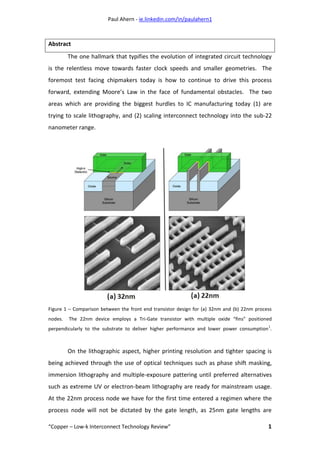
1. Paul Ahern - ie.linkedin.com/in/paulahern1
“Copper – Low-k Interconnect Technology Review” 1
Abstract
The one hallmark that typifies the evolution of integrated circuit technology
is the relentless move towards faster clock speeds and smaller geometries. The
foremost test facing chipmakers today is how to continue to drive this process
forward, extending Moore’s Law in the face of fundamental obstacles. The two
areas which are providing the biggest hurdles to IC manufacturing today (1) are
trying to scale lithography, and (2) scaling interconnect technology into the sub-22
nanometer range.
Figure 1 – Comparison between the front end transistor design for (a) 32nm and (b) 22nm process
nodes. The 22nm device employs a Tri-Gate transistor with multiple oxide “fins” positioned
perpendicularly to the substrate to deliver higher performance and lower power consumption
1
.
On the lithographic aspect, higher printing resolution and tighter spacing is
being achieved through the use of optical techniques such as phase shift masking,
immersion lithography and multiple-exposure pattering until preferred alternatives
such as extreme UV or electron-beam lithography are ready for mainstream usage.
At the 22nm process node we have for the first time entered a regimen where the
process node will not be dictated by the gate length, as 25nm gate lengths are
2. Paul Ahern - ie.linkedin.com/in/paulahern1
“Copper – Low-k Interconnect Technology Review” 2
typical, and also where the historic 2D planar design of transistor has been replaced
by a 3D “Tri-gate” design by companies such as Intel2
and AMD – with close to 3
billion transistors present on Intel’s Ivy bridge family of CPUs (see figure 1).
Meanwhile, on the interconnect side, the challenge is to adequately route
the signal into and out of the transistors in the device front-end while keeping pace
with increases in speed and packing density and also sidestepping the problems of
latency due to Resistive-Capacitive (RC) delay.
This review paper will focus on the development of interconnect technology,
from the SiO2 / aluminium system into the low-k/copper process node, and detail the
path forward for ever-shrinking process geometries which are fabricated for the first
time in all three dimensions.
From Aluminium to Copper
Aluminium has served the semiconductor industry well as a back-end metallisation
medium. Robert Noyce, then of Fairchild Semiconductor but later to be a co-founder
of Intel, filed his patent describing the “Semiconductor Device & Lead Structure3
”
approach in 1957. Noyce was the first to conceive using deposited aluminium metal
lines to connect transistors, diodes and other devices on the surface of a monolithic
piece of silicon, and aluminium remained the metallisation of choice up until the
0.18µm process node.
Aluminium can be deposited by Physical Vapour Deposition (PVD) or
Chemical Vapour Deposition (CVD) methods, giving a layer with sufficiently low
resistivity and good adherence to SiO2. Later, copper was added as an alloying
material in concentrations of up to 0.5 atomic percent, in order to improve the
electromigration lifetime of the conductor through the mechanisms of reduced
electron mobility and pinning defects at the grain boundaries4
.
3. Paul Ahern - ie.linkedin.com/in/paulahern1
“Copper – Low-k Interconnect Technology Review” 3
Figure 2 – (Left) SEM isometric view and (right) cross-section view of a 10 level copper metallised
integrated circuit
5
.
The 1994 edition of the pan-industry “National Technology Roadmap for
Semiconductors” (NTRS) was the first to focus on the upcoming need for new back-
end conductor materials and low-k dielectrics to satisfy the anticipated device
scaling and power requirements6
. As aluminium began to run out of steam, copper
was seen as its natural successor as an interconnect material due to its good
combination of material properties: high conductivity, low resistivity, ease of
deposition using the existing process methods, and having high electromigration
resistance.
There are also some inherent problems with copper such as its tendency to
corrode due to the absence of a self-passivating layer like that formed by aluminium,
and its questionable adhesion characteristics. In addition, new processing steps that
would be required to accommodate its inclusion in the fabrication process such as
damascene processing, electrochemical plating and chemical mechanical polishing
(CMP). Also, due to coppers tendency to diffuse into SiO2, cobalt or tungsten (and its
silicides) must be used instead of copper as the initial contact via layer where the
first metal layer connects into the transistor gate.
4. Paul Ahern - ie.linkedin.com/in/paulahern1
“Copper – Low-k Interconnect Technology Review” 4
Copper Patterning & the “Damascene” Methodology
One process change necessitated by the inclusion of copper as a back end metallic is
that dry etch processes, long utilised for aluminium, must be redesigned. These
subtractive etch chemistries are no longer viable with copper as the necessary etch
chemistries required cannot be generated within the acceptable thermal budget of
the fabrication process. Chemical Mechanical Polishing (CMP) is instead used to
planarise the surface of the wafer after copper has been laid down on the surface.
The term “damascening” has its roots in antiquity as a method for inlaying
patterned metals, typically gold or silver, into an object for purely aesthetic reasons.
In the world of integrated circuits, damascene is the process where copper layers are
patterned into an insulative substrate – dual damascene being where the vias and
the metal lines are deposited in one combined process step. A dual damascene
methodology has several advantages, such as its lower cost, lower via resistances
(due to the monolithic nature of the via-metal line stack), and faster processing time
with less process steps to monitor. Disadvantages are mainly due to the complexity
of controlling such a convoluted process and limitations on the aspect ratios that can
be filled by a one-step electroplating route7
.
Figure 3 – A diagrammatical representation of a standard “Via-First” dual-damascene process
8
.
5. Paul Ahern - ie.linkedin.com/in/paulahern1
“Copper – Low-k Interconnect Technology Review” 5
As shown in figure (3) previously, the via-first process starts at (a) with the
deposition of an interlayer dielectric (ILD). A photoresist layer is applied and
patterned in step (b) and the via structures are etched in step (c). After the resist
has been “ashed” or cleaned in step (d), another layer of resist is applied (e) which
patterns the locations for the metal lines. The lines are etched in step (f), with the
dark blue layer in the diagram representing a previously deposited embedded etch
stop layer which is usually composed of silicon nitride, the resist removed in step (g).
A barrier layer is applied in step (h) whose purpose is to promote adhesion of the
subsequent copper seed layer to the underlying ILD material and also to act as a
shunt layer to prevent electromigration. In step (i), copper fills the via/line trench
from the bottom up by a process of electroplating with additives, and in step (j) the
overhanging copper which is in excess from the electroplating process is planarised
back by a process of chemical mechanical polishing (CMP).
Deviations from Via-First Dual Damascene Processing
Variations on the via-first process are available: trench-first dual damascene
processing, as the name implies, flips the process so that the metal lines are
patterned first, the exposed resist layer removed, and then the remaining resist layer
is used to pattern the vias. The main disadvantage of this method is that via
lithography must be done on a resist surface which has already been cleaned and
can be quite rough. This results in slightly lower achievable minimum via sizes than
in the via-first scheme, meaning that below the 0.25µm process node the benefits of
a trench-first process are negligible9
.
Meanwhile, self-aligned (or “buried”) dual damascene is an interesting
variation which has not as yet found widespread acceptance in the semiconductor
manufacturing community. Patented by AMD in 199510
, the process works by
patterning the vias in the embedded etch stop layer before the second half of the ILD
is laid down with the trench pattern, and then both the via and trench are opened up
simultaneously with one etch step. While a perfectly controllable self-aligned
process would offer many advantages in terms of process simplification, the
disadvantages are that via-trench alignment is absolutely critical and misalignment
6. Paul Ahern - ie.linkedin.com/in/paulahern1
“Copper – Low-k Interconnect Technology Review” 6
can give vias which do not have a circular appearance, and also an etch process with
very high oxide:nitride selectivity is needed11
.
Interlayer Dielectrics Overview
The interlayer dielectric or “ILD” layer is used to insulate conductive metal
layers from one another to prevent shorting of the semiconductor device. As the
feature size of integrated circuits decreases into the nanometre range, the limiting
factor of integrated circuitry shifts from the traditional front-end attributes of gate
length and gate thickness, to back-end properties such as the conductivity of the
metal lines and interconnect layers, the parasitic capacitance and resistance of the
ILD materials, and the compatibility and mechanical properties of these new
materials. As such, low-k materials have a large part to play in the semiconductor
industries goal of extending Moore’s law for as long as feasibly possible.
Electrical Properties Mechanical Properties Thermal Properties
Low dielectric constant
Low dielectric loss
Low leakage current
No incorporated charges
High reliability
Good adhesion
Low shrinkage
Crack resistant
Low film stress
Sufficient hardness
Thermal stability
Low coefficient of
expansion
Low shrinkage
Sufficient heat
conductivity
Chemical Properties Processing Properties Metallisation Properties
Resistant to acids and
bases
High etch selectivity
Low impurity levels
No corrosion
Low moisture uptake
No outgassing
Long storage life
Environmentally safe
Good Patternability
Good gap fill
properties
Good planarisation
uniformity
Good deposition
uniformity
Low pinhole rate
Low particulate
count
Low cost of
ownership
Low metal temperature
Compatible with
diffusion barriers
Low contact resistance
Good electromigration
performance
Low level of stress
voiding
Absence of hillock
formation
Figure 4 – An idealised “shopping list” of criteria which a successful ILD material must
demonstrate12
.
7. Paul Ahern - ie.linkedin.com/in/paulahern1
“Copper – Low-k Interconnect Technology Review” 7
The main reason that dielectric materials have come under the research
spotlight is due to their effect on device speed. At a process node size of 0.18µm
and above, the ILD layers acted as insulators but also provided important structural
support to the metal layers on the wafer. However, below the 180nm process node,
the intrinsic electrical and physical properties of the ILD material is much more
important13
. RC, or interconnect, delay now exceeds the gate delay of devices, and
its influence is even more prominent when the number of layers of metal lines, and
consequently the number of ILD layers, is increased. Resistance [R] can be
decreased by moving from aluminium to copper metallisation, and capacitance [C] is
reduced by the introduction of new ILD materials. Another concern is that, in order
to reduce dielectric heating, the capacitance must be further reduced by using
materials with a low dielectric constant (k) value – as high temperatures inside an
operating device can quickly lead to failure due to electromigration, diffusion of
implant regions and dielectric breakdown.
Type Interlayer Dielectric (ILD) materials Dielectric Constant (k)
Oxide Derivatives SiO2 3.9
SiOF (CVD) 3.5
Carbon doped oxide (CDO) films of
Hydrogen Silsesquioxane (HSD)
Methylsilsesquioxane (MSQ)
2.9 ~ 2.5
Organic Materials Fluoropolymide (spin-on) 2.8
Benzo-cyclo butene 2.7
Polyethylene 2.4
Polypropylene 2.3
Fluoropolymer 2.24
Parylene-F 2.2
PTFE (spun-on “Teflon”) 2.1 ~ 1.9
Highly Porous Oxides Aerogels & xerogels 2.5 ~ 1.8
Air 1
Figure 5 - Proposed CVD plasma deposited materials for future semiconductor fabrication
processes14
, 15
.
8. Paul Ahern - ie.linkedin.com/in/paulahern1
“Copper – Low-k Interconnect Technology Review” 8
Low-k Materials: Moving Beyond SiO2
Early contenders as a replacement for SiO2 were fluorine-based organic
polymers16
, SiO2-based inorganic oxides 17
and porous materials18
. Low-k dielectric
materials require some specific material properties as well as the prerequisite
electrical properties - these include the ability of the material to be deposited in a
low thermal budget scheme, to fill into narrow, deep metal layer interconnect gaps
without void formation, to be uniform in density to facilitation uniform planarisation
of the layer during chemical mechanical polishing (CMP) and have a high resistance
to moisture absorption from the atmosphere19
by possessing good barrier
hermeticity.
SiOF or FSG (Fluorinated Silicon Glass) became popular in the semiconductor
industry as it offered a rapid, step-wise integration into the standard SiO2 ILD regime,
and could be deposited using the standard PECVD or HDP-CVD deposition toolset.
The incorporation of Fluorine into amorphous SiO2 films reduces the film dielectric
constant and offers a film of high density and high thermal stability, and all this with
an appreciable decrease of the dielectric constant of the ILD layer from k 4 for SiO2
to k 3.5 for the plasma-deposited SiOF layers20
.
For all these reasons, doped ILD layers quickly became prevalent in any
semiconductor design where the patterning size was at or under 130nm where the
speed of signal propagation was important, giving a faster switching transistor device
with the added benefit of lower power consumption, with the added benefit of
reduced “cross-talk” between metal layers.
A further advantage was that the incorporation of fluorine into the ILD
introduced an etching character to the material during the deposition process. This
enhances the “gap-filling” capability of the film and allows metal lines with narrower
pitches to be conformally covered with a lesser instance of voiding. This allowed a
cost advantage as it resulted in more metal lines in a smaller area on the device
being fabricated21
.
The first wave of 180nm products that arrived at the end of 1999 contained
regular silica or fluorinated silicate glass (FSG) layers, with a range of dielectric
constant values between 3.7 and 4.2. The SiOF layers were deposited by various
9. Paul Ahern - ie.linkedin.com/in/paulahern1
“Copper – Low-k Interconnect Technology Review” 9
techniques such as PECVD using carbon fluorides, room temperature catalytic CVD
and electron cyclic resonance (ECR) plasma CVD. The announcement by IBM that it
was to pioneer Copper metallisation in its PowerPC 750 chip product increased
doubt in the industry about the readiness and need for low-k ILD layers. The modest
decrease in RC delay achieved by using copper only served to postpone the
development of the low-k materials by one process generation.
Migration to Carbon-Doped Oxides (CDO)
With the industry switching to copper metallisation, and 300mm wafer sizes
in order to take advantage of economies of scale, an opportunity presented itself to
usher in a new type of ILD material. At the time, the front-runner for next
generation 130nm process geometries was “SiLK”, a spin-on aromatic polymer
manufactured by Dow Chemical containing 60 at% Carbon, 39 at% Hydrogen and 1
at% Oxygen, but no Silicon. SiLK promised an attractive dielectric constant decrease
of k 2.7, but was expensive and required many complicated process tweaks to
integrate it, including mineral hard mask layers for polishing and adhesion reasons.
There were also reliability concerns with SiLK when integrated into a copper
metallisation scheme, with poor electromigration performance seen when compared
to the traditional Cu/SiO2 based regime.
Enter carbon–doped oxide (CDO), which built upon the fluorinated silicon
dioxide model and gave a more modest k decrease of 2.8 but crucially could be
deposited using well-understood plasma enhanced chemical vapour deposition (PE-
CVD) tools. The plasma processing initially left a damaged and strained film on the
wafer surface, but post-processing plasma treatments and thermal annealing
processes were developed that could be used to reduce these artefacts and give a
useable film22
.
Effect of Doping on the Dielectric Constant of SiO2
There are many theories as to the influence of doping on the dielectric constant of
SiO2. One or more of the following models may responsible for the decrease in k by
dopant species incorporation.
10. Paul Ahern - ie.linkedin.com/in/paulahern1
“Copper – Low-k Interconnect Technology Review” 10
Film Porosity: A model by Han23
and Aydil states that that incorporation of a dopant
species leads to a less dense, more porous film with controlled void formation.
Hydroxide Substitution: A model first proposed by Lim24
and co-workers that the
dopant displaces relatively more polarisable molecules such as SiOH in the film, thus
reducing the dielectric constant.
Silicon Oxide Bond Substitution: A model put forward by Shapiro25
and co-workers.
The belief is that Si-O bonds within the SiO2 matrix are replaced with Si-F bonds
which reduces the total polarisability of the matrix and hence lowers the electronic
contribution of the dielectric constant. Also, a further theory by Lim26
and co-
workers expands on this model with the idea that incorporation of Si-F or SiOF bonds
in the place of Si-O bonds reduces further the ionic character of the matrix and thus
the dielectric constant of the total film.
For carbon doped oxides, Ding & co-workers27
showed that an increase in the
cross-linking in the structure due to increased number of C-O and C-F bonds leads to
a lower observed dielectric constant value which varies strongly with the amount of
carbon and fluorine in the pre-cursor gases28
.
Process Control With Low-k Dielectrics
One of the challenges with carbon doped oxides concerns process control,
with many laboratory techniques used to control the electrical and mechanical
properties of the film. Dynamic Secondary-Ion Mass Spectroscopy (SIMS) is used to
monitor the carbon levels within the bulk of the film by depth profiling as well as the
crucial surface layers where carbon depletion can be an issue if the wafer is allowed
to sit under ambient pressure for too long. This can be remedied by the addition of
an adventitious surface layer of fluorocarbons on the carbon doped oxide surface by
varying the plasma chemistry to a slightly less oxygen-rich composition29
. Any post-
treatment needs to also monitor carefully any shrinkage in the film which could
adversely affect downstream lithographic steps in the process.
11. Paul Ahern - ie.linkedin.com/in/paulahern1
“Copper – Low-k Interconnect Technology Review” 11
Figure 6 – Some of the common process integration challenges involved in the Copper/low-k system
30
.
Moisture content and the rate of water uptake is a critical concern for low-k
dielectric films. A revealing study by Cheng et al31
showed that in FSG films (Fluoro-
Silicate Glass), the water absorption rate increases with increasing fluorine content.
High fluorine concentrations, which should give the lowest dielectric constant value,
are thus not utilised due to poor film stability as they absorb atmospheric water.
SiOF films with fluorine contents over 5 at% fluorine can expect to lose about 0.5 at%
after a week exposed in the cleanroom environment.
Moisture absorption and fluorine displacement increases rapidly for films
with higher at% F. Similarly, in carbon doped oxide films it was found that plasma
post-treatments usually lead to an increase in moisture uptake from the local
environment and a subsequent loss in carbon from the material due to substitution,
with the expected increase in k value32
.
For carbon doped oxides the presence of so-called “caged” SiO bonds in a
matrix composed of separate Si-O-Si and Si-O-C bonds has been put forward as being
responsible for the properties of the CDO film33
. Deliberately inducing pores into the
material allows a further decrease in the k value down to ~2.1.
12. Paul Ahern - ie.linkedin.com/in/paulahern1
“Copper – Low-k Interconnect Technology Review” 12
Interaction Between Low-k Dielectrics & Metal Layers / Oxides.
From the point of view of process control and integration, one of the most important
requirements is that the dopant from the low-k layer remain stationary and not
diffuse into other layers. This is difficult with SiOF as Fluorine is one of the most
mobile atoms; diffusion of F into metal layers will give rise to a corrosive interaction
with parts or all of the metal stack.
Work undertaken by Passemard and co-workers34
directly linked the level of
Fluorine to the level of corrosion in metal lines fabricated in a Ti/TiN/AlCu/TiN
regime. Visual inspection showed that below 3.4 at% Fluorine there was no
corrosion, but between 3.4 and 5 at% fluorine corrosion increased in the Ti/TiN
layers. Above 5 at% Fluorine the corrosion started to affect the AlCu layer also.
In all cases the corrosion begins at the outside edges of the metal lines.
In addition to this work, Choi and co-workers reported that the corrosion occurred in
the barrier layers (Ti and TiN) but not in the Al layers themselves35
. Labiadh’s
studies36
on Copper metal layers and SiOF dielectrics showed that there was no
diffusion from the SiOF into the copper layer or vice versa, but that F could be seen
in the Ti and TiN barrier layers.
Surmounting the Mechanical Adhesion Problem
One huge issue with the copper – low-k system is that the reliability and
robustness of the processing of such materials is strongly dependent on the
mechanical adhesion between layers in the back end of the process. While copper is
an improvement over aluminium in terms of its resistance, copper suffers from lower
adhesion compared to aluminium. This necessitates an understanding of its
behaviour in interaction with other materials it will come into contact with during
semiconductor processing37
.
13. Paul Ahern - ie.linkedin.com/in/paulahern1
“Copper – Low-k Interconnect Technology Review” 13
Figure 7 – SEM images showing the result of a four-point bending test on a carbon doped oxide –
copper IC. Sample (a) displays poor adhesion, sample (b) good adhesion. The crack dimensions can
be measured and used to understand the mechanisms for crack initiation & propagation
38
.
The mechanical adhesion and the dielectric constant of the film have an
inversely proportional relationship. Adhesion can be measured by four-point bend
testing to measure the dissipation of surface energy when a crack is propagated
along the CDO to copper interface, or it can be calculated from cross-sectional
nanoindentation39
of the film coupled with an understanding of its material
properties such as the Young’s Modulus. The dielectric constant can be measured by
using a standard four point probe, or by a more complicated mercury probe system
in which a blob of mercury is used as a temporary metal gate to form a parallel plate
capacitor system where conductance and K values can be read, usually in the form of
an “in-line” metrology step with the wafer fab. Targeting the K value too low leads
to issues with mechanical strength, film adhesion, low uniformity across the wafer
and voiding in the ILD film.
ILD Materials for 22nm Process Node & Below
The relentless march towards smaller feature sizes requires continued
materials & process research in order to forestall the much-mooted demise of
Moore’s Law. For low-k materials, the ability to continually reduce the intrinsic k
value of a monolithic thin film is becoming more and more challenging, and so the
easiest route seems to be the introduction of some porous character to existing
materials to further decrease RC delay. There are a huge number of potential
options being evaluated at present, with everything from porous silicate glass to
14. Paul Ahern - ie.linkedin.com/in/paulahern1
“Copper – Low-k Interconnect Technology Review” 14
aerogels being considered and piloted. It appears that the age of spin-on low-k
materials may have finally arrived after their shortcomings for carbon-doped oxides,
with porous SiLK now again being evaluated.
Many materials use some version of a sol-gel process to achieve a spin-on
material which is then exposed to a solvent to give an ordered, 3D network by
polymerisation and which has an easily-controlled pore size. Of critical importance
here is the distribution of pore sizes in the material, as a structure with open pores
and a wide variety of pore sizes will have poor mechanical strength rendering it
unusable in real-world processing conditions.
ATM Incorporated, in conjunction with fab equipment vendor ASM
International, have developed and patented40
the ability to produce porous, stable
carbon doped oxide films with k values of ~2 through a process of plasma-enhanced
CVD using precursors of cyclic siloxane and a pore-forming polymer species with a
thermally-cleavable organic group, termed a “porogen”. The porogen is a sacrificial
material which is then removed by UV curing to give a resultant film with adequate
mechanical strength, well-controlled pore size distribution and a pore fraction of
42% and a mean pore size of 3.3nm41
.
IBM, a long-standing leader in the low-k field, has shown details of their
solution, dubbed “post porosity plasma protection” or “P4” scheme. The film uses a
bridged oxy-carbosilane material which has open pores which are then charged with
an organic material prior to patterning and thermally removed at the end of the
process step. This solution is readily integrated with existing copper dual-damascene
processing and minimises Plasma-Induced Damage (PID) to the film which can be
caused by aggressive oxygen etch chemistries to porous materials.
15. Paul Ahern - ie.linkedin.com/in/paulahern1
“Copper – Low-k Interconnect Technology Review” 15
Figure 8 – IBM’s “P4” process, which stands for “Post Porosity Plasma Protection”, promises
a film with sufficient mechanical strength to withstand CMP. The filler material is then removed
afterwards to give open pores
42
.
The endgame for low-k materials is ultimately their elimination, replacing
them with a porous “air-gap” which will have a k value of ~1 and excellent reliability
in terms of enhanced gate leakage current, cross-talk and electromigration
performance. A major challenges is how to accurately self-align the air pocket
between the vias and trenches being patterned by the existing dual damascene
processing without the use of a mask layer. Conserving the mechanical integrity of
the device is also critical so that it can survive chemical-mechanical polishing and
adequately seal the internal air gaps to prevent any ingress of contamination.
To this end, many research groups43
are focussing on the use of some kind of
sacrificial material to form the air gap, and then once the copper lines have been
formed, this material can be completely removed to give aligned air cavities. The
main problem with this approach is that the overall thermal budget of the process
might not allow for the high-temperature processes needed to cleanly remove the
sacrificial material.
16. Paul Ahern - ie.linkedin.com/in/paulahern1
“Copper – Low-k Interconnect Technology Review” 16
Figure 9 – Cross-section diagram of how air gaps can be achieved in a dual damascene process.
Conventional carbon doped oxide (SiOC) is deposited and allowed to pinch closed at the opening at
the top of the metal trench, leaving an appreciable amount of ILD material for mechanical support
and to act as a chemical barrier layer
44
.
Copper Metallisation Beyond 22nm
The move towards air gaps brings with it a slew of challenges for the metallic parts of
the back-end process. Long-standing Chemical Vapour Deposition (CVD) methods
which have been successfully employed for decades, and even the relatively recent
Physical Vapour Deposition (PVD) techniques which were implemented at the 45nm
process node are suddenly faced with the possibility of being unable to fill the sub-
14nm metal trenches which are on the horizon. They require the deposition of
barrier layers which may be only 15Å, or three atomic layers, thick. Similarly, the
vast improvements that have been made in copper electroplating which have
allowed this technique to continue to be relevant, even at current process
geometries, must begin anew in order to keep pace with the need for highly
selective bottom-filling of vias and trenches of ever-smaller sizes.
Academia, equipment suppliers and the semiconductor industry has in turn
begun to look at new techniques such as Atomic Layer Deposition (ALD) coupled with
new metallic species to act as conductors. ALD allows for the deposition of
conformal layers which are only as thick as a single atom, in a very slow and
17. Paul Ahern - ie.linkedin.com/in/paulahern1
“Copper – Low-k Interconnect Technology Review” 17
controllable method, but it is thought that CVD may offer higher-purity films with
better conformal step-coverage.
Figure 10 – Diagram of an atomic layer deposition (ALD) process
45
. Very thin films can be laid down
by the successive use of a gas phase elemental deposition. The ultimate film thickness is governed by
the amount of ALD series, so thickness control is both precise and straightforward.
The currently-used Ta/TaN seed & barrier layer stack is likely to be replaced
with cobalt46
or ruthenium47
deposited by either ALD, CVD or a combination of both.
Ruthenium offers better wettability and adhesion with copper, but has poorer
polishing characteristics when it comes to CMP – conversely, cobalt is easier to
polish but is not an ideal barrier layer to stop the migration of oxygen, which means
long term reliability from corrosion and oxidation may suffer. Another issue is
electromigration performance48
, although cobalt would appear to offer advantages
here as a recent paper demonstrates49
. The authors show that cobalt films
deposited by CVD onto copper lines show a significant enhancement in
electromigration performance over time, which is critical as at smaller feature sizes
the gate region can be spanned and shorted by the presence of only a few atoms of
contamination.
18. Paul Ahern - ie.linkedin.com/in/paulahern1
“Copper – Low-k Interconnect Technology Review” 18
Figure 11 – Right
50
: Log scale of electromigration failure time comparing samples with & without a
cobalt capping layer. Left: Cross-section STEM image of a copper interconnect with cobalt cap. EDX
mapping below shows the distribution of tantalum, copper and cobalt in the via and its sidewalls.
Conclusion
Moving from aluminium to copper as an interconnect metal has provided many
advantages for semiconductor manufacturers, but has not been without its pitfalls.
New, complex process steps have been introduced in order to adapt the IC
manufacturing flow to accommodate copper and its characteristics; CMP, seed layer
deposition technology, improvements to electroplating bath chemistries and novel
etch steps have all been necessary. Improvements in low-k dielectric materials have
allowed the disruption of the inherent back-end speed bottleneck in semiconductor
devices to be mitigated. The result of even faster devices of smaller geometries have
extended Moore’s Law successfully for many process generations – however,
continual improvements are essential if the industry is to scale devices below the
crucial 22nm process node.
19. Paul Ahern - ie.linkedin.com/in/paulahern1
“Copper – Low-k Interconnect Technology Review” 19
References
1
M. Bohr & K. Mistry, “Intel’s Revolutionary 22nm Transistor Technology”
http://download.intel.com/newsroom/kits/22nm/pdfs/22nm-Details_Presentation.pdf; retrieved
21/11/2012.
2
M. Bohr & K. Mistry, ibid.
3
Noyce, Robert N., "Semiconductor Device-and-Lead Structure”, Reprint of U.S. Patent 2,981,877
(Issued April 25, 1961. Filed July 30, 1959), Solid-State Circuits Newsletter, IEEE, vol.12, no.2, pp.34-
40, (2007).
4
May, G.S. & Sze, S.M., “Fundamentals of Semiconductors Fabrication”, John Wiley & Sons (2004).
5
Edelstein, D. et al "Reliability, yield, and performance of a 90 nm SOI/Cu/SiCOH technology",
Proceedings of the IEEE 2004 International Interconnect Technology Conference, pp. 214- 216 (2004).
6
Rathore, H. S. & Chandra, K. “Chapter 4 - Copper, low-k dielectrics, and their reliability” from
“Semiconductor Manufacturing Handbook” editor Hwaiyu Geng, McGraw Hill (2005).
7
Dixit, G. A. & Havemann, R. H. “Overview of the Interconnect-Copper and Low-k Integration” chapter
from “Handbook of Semiconductor Manufacturing Technology, Second Edition” Edited by Robert
Doering and Yoshio Nishi, CRC Press (2007).
8
Weng, C. J. “Systematic defect improvement integration of dual damascene processes development
on nano semiconductor fabrication”, Materials Science in Semiconductor Processing, Vol. 13, Issues
5–6, pp. 376-382 (2010).
9
Wolf, S. “Introduction to dual-damascene interconnect processes” chapter from “Silicon Processing
for the VLSI era” Vol. 4 pp. 674-679, Lattice Press (2004).
10
US Patent Number 5,614,765 “Self-Aligned Via Dual Damascene” Avanzino et al.
http://www.google.co.uk/patents/US5614765, retrieved 3/12/2012.
11
Wolf, S. ibid.
12
After table presented in Semiconductor International Vol. 20 Issue 8 pp. 126 (1997).
13
May, G.S. & Sze, S.M., “Fundamentals of Semiconductors Fabrication”, John Wiley & Sons (2004).
14
After “The Future of Dielectric CVD High Density Plasmas”, Peter Singer, Semiconductor
International magazine (1997).
15
Saraswat, Prof. K. “Low-k Dielectrics” course notes, Dept. of Electrical Engineering, Stanford
University. http://www.stanford.edu/class/ee311/NOTES/Interconnect%20Lowk.pdf retreived
26/11/2012.
16
Muranka, S. P. “Fluorinted Silicon oxide glasses”, Solid State Technology, Vol. 38, pp. 83-88 (1996).
17
Fukuda, T. et al “Proceedings of the third international dielectrics for VLSI/ULSI Multilevel
Interconnection Conference” pp. 41 (1997).
18
Hendricks, N. H. “Solid State Technology” Vol. 38 pp. 117 (1995).
19
Kalkman, A.J. et al “SiOF and SiO2 deposition in an ECR-HDP reactor: Tool characterisation and film
analysis”, Microelectronic Engineering Vol. 37/38pp. 271-276 (1997).
20. Paul Ahern - ie.linkedin.com/in/paulahern1
“Copper – Low-k Interconnect Technology Review” 20
20
Reynard, J. "Integration of fluorine-doped silicon oxide in copper pilot line for 0.12-μm technology".
Microelectronic Engineering, Vol. 60, 113 (2002)
21
Homma, T. “Fluorinated interlayer dielectric films in ULSI multilevel interconnections” , Journal of
Non-crystalline Solids, Vol. 187 pp. 49-59 (1995).
22
Wang, Y. H. et al, Electrochemical & Solid-State Letters, Vol. 6, F1 (2003).
23
Han, S. M. & Aydil, E. S., Journal of Vacuum Science & Technology (A), Vol. 15 pp. 2893 (1997).
24
Lim, S. W. et al, Journal of Electrochemistry Society, Vol. 144 pp. 2531 (1997).
25
Shapiro, M. J. et al, Journal of Thin Solid Films, Vol. 270 pp. 503 (1995).
26
Lim, S. W. et al, Japan Journal of Applied Physics, Vol. 35 pp. 1468 (1996).
27
Wang, P.F. et al “An amorphous SiCOF film with low dielectric constant prepared by plasma-
enhanced chemical vapor deposition”, Thin Solid Films, Vol. 385, pp. 115-119 (2001).
28
Ding, S.J. et al “Structure characterization of carbon and fluorine-doped silicon oxide films with low
dielectric constant”, Materials Chemistry & Physics, Vol. 71, Issue 2, pp. 125-130 (2001).
29
I. Reid et al, “Suppression of carbon depletion from carbon-doped low-k dielectric layers during
fluorocarbon-based plasma etching” Microelectronic Engineering Vol. 83, Issues 11–12, pp. 2458–
2461 (2006).
30
Jan, C.H., IEDM Short Course (2003).
31
Cheng, Y. L. et al “Characterization and reliability of low dielectric constant fluorosilicate glass and
silicon rich oxide process for deep sub-micron device application” Thin Solid Films, Vol. 398 – 399 pp.
533–538 (2001).
32
Wangz, Y. H. & Kumar, R. “Stability of Carbon-Doped Silicon Oxide Low-k Thin Films” J. Electrochem.
Soc. Vol. 151, Issue 4, F73-F76 (2004).
33
Yang, C.S. et al “The influence of carbon content in carbon-doped silicon oxide film by thermal
treatment”, Thin Solid Films, Vol. 435, Issues 1–2, pp. 165-169 (2003).
34
Passemard, G. et al “Study of fluorine stability in fluoro-silicate glass and effects on dielectric
properties”, Microelectronic Engineering, Vol. 33, pp. 335-342 (1997).
35
Choi, J. H. et al “IEEE VMIC Conference Reports”, pp. 397 (1995).
36
Labiadh, A. “Study of the thermal stability at the Cu/SiOF interface”, Microelectronic Engineering,
Vol. 33, Issues 1-4 pp. 369-375 (1997).
37
Felder, Eric et al “Characterization of the adhesion of thin film by Cross-Sectional Nanoindentation
Analysis of the substrate edge chipping and the film delamination” Comptes Rendus Mecanique, Vol.
339, pp. 443 – 457 (2011).
38
Molina-Aldareguia, J.M. et al “Adhesion studies in integrated circuit interconnect structures”,
Engineering Failure Analysis, Vol. 14, Issue 2, pp. 349-354 (2007).
21. Paul Ahern - ie.linkedin.com/in/paulahern1
“Copper – Low-k Interconnect Technology Review” 21
39
Sánchez, J.M. et al “Cross-sectional nanoindentation: a new technique for thin film interfacial
adhesion characterization”, Acta Materialia, Vol. 47, Issue 17, pp. 4405-4413 (1999).
40
Xu, C. “Porogen Material for ultralow-k dielectrics” US Patent Number 7,456,488 B2,
http://assignments.uspto.gov/assignments/q?db=pat&pat=7456488 retrieved 27/11/2012.
41
LaPedus, M. “Challenges Mount For Interconnects” Semiconductor Manufacturing & Design,
http://semimd.com/blog/2012/06/26/challenges-mount-for-interconnect/, retrieved 27/11/2012.
42
Frot, T. et al “Post Porosity Plasma Protection - a new approach to integrate k ≤ 2.2 porous ULK
materials” Interconnect Technology Conference & 2011 Materials for Advanced Metallization
(IITC/MAM), IEEE International (2011).
43
Gosset, L. G. et al “General review of issues and perspectives for advanced copper interconnections
using air gap as ultra-low K material”. Proceedings of the IEEE 2003 International Interconnect
Technology Conference (2003).
44
Korczynski, E. “IEDM Shows Air-gaps By Design” news article on Semiconductor Manufacturing &
Design, http://semimd.com/blog/2011/02/05/iedm-2010-shows-air-gaps-for-real/ retrieved
26/11/2012.
45
Wang, H. et al, "Atomic Layer Deposition of Lanthanum-Based Ternary Oxides," Electrochemical &
Solid-State Letters Vol. 12 (4), G13-G15 (2009).
46
Kim, H. et al “Applications of atomic layer deposition to nanofabrication and emerging
nanodevices”, Thin Solid Films, Vol. 517, Issue 8, pp. 2563-2580 (2009).
47
Gebregziabiher, D. K. et al “Electrochemical atomic layer deposition of copper nanofilms on
ruthenium”, Journal of Crystal Growth, Vol. 312, Issue 8, pp. 1271-1276 (2010).
48
Yang, C.-C. et al "Characterization of Copper Electromigration Dependence on Selective Chemical
Vapor Deposited Cobalt Capping Layer Thickness," Electron Device Letters, IEEE , Vol.32, no.4, pp.560-
562 (2011).
49
Yang, C.-C. et al, “Co capping layers for Cu/low-k interconnects”, Microelectronic Engineering, Vol.
92, pp. 79-82 (2012).
50
Yang, C.-C. et al, ibid.