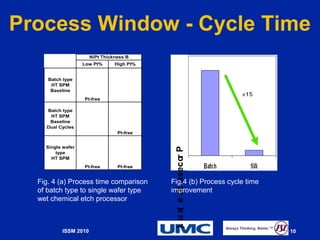
SlideShare a Scribd company logo
ISSM 2010      NiPt SALICIDE Process
                      Optimization for
                 28nm CMOS Manufacturing


                        James M.M. Chu (Speaker)
                        Application Dept. Manager
                        SE Asia/Greater China Region
                        FSI International

                        James.chu@fsi-intl.com

            ISSM 2010                                  1   G-Number
NiPt Silicide for CMOS
      Source                Gate    Drain                      Scaling

                            NiSi


                                     Contact electrode
        Contact electrode

                                                                NiSi         65nm


                                                                NiSi         45nm
                            Gate
                            Stack

                                                                 NiSi        28nm
       NiSi                         NiSi
STI                                                      STI
                             Si

         ISSM 2010                                                       2    G-Number
NiSi Encroachment Defects

 Spiking


  Piping


65nm node and beyond : Ni(Pt 5-10%) replace Ni for defect control.
But … residual surface Pt removal become a challenge !!!

         ISSM 2010                                            3   G-Number
Motivations
 Tostay with current material (NiPt) and
 chemistry (SPM) for SALICIDE formation

 To   scale NiSi into 28nm CMOS device

 To   optimize wet selective etch process
  – Support the residual NiPt removal on the film
    thickness and Pt% proposed
  – Reduce the process cycle time


       ISSM 2010                                    4   G-Number
NiPt Salicide Process
 Process    Flow (Fig.1)

    Surface preparation: wet + dry in-situ
    Metal Dep.: Ni(Pt) + TiN cap→ main focus of this presentation
    1st Anneal (RTP-1): 200-300°C range
    Selective wet etching→ main focus of this presentation
    2nd Anneal (RTP-2): > 500°C
    Defect inspection: SEM e-beam BVC inspection


    WAT Measurement: Sheet Resistance / Uniformity


       ISSM 2010                                             5   G-Number
Pt Reaction Model
 Common        Pt reaction model
  - Aqua regia base :
      Pt + 4NO3- + 8H +  Pt(4+) + NO2 + 4H2O                 Silicide
     Pt(4+) + 6Cl - + 2H +  H2PtCl6                         Attacked !

  - Hydrochloric acid base :
      Pt + 2H2O2 + 4H +  Pt(4+) + 4H2O
           Pt(4+) + 6Cl - + 2H +  H2PtCl6

  Sulfuric          Acid Peroxide Pt reaction model
  - Sulfuric acid base (main focus of this presentation)      Take place
      Pt + H2SO4 + H2O2  Pt(OH)2++ + PtO++ + H2SO3               On
                                                           high temperature


         ISSM 2010                                                 6   G-Number
Batch/SW
Processor Comparison
               HT SPM


                                         HT SPM

 wafers        wafers

                                 wafer


     Closed chamber              Closed chamber

Fig.2(a) Batch wafer type   Fig.2(b) Single wafer type


 ISSM 2010                                               7   G-Number
Pt% / NiPt Film Optimization
         on Rs/BVC
                                                                         increasing film thickness
 BVC Count (a.u.)


                                                      BVC Count (a.u.)
                                      x15


                    Low Pt %
                      5% Pt
                               NiPt Film  High Pt %
                                            10% Pt                          A                        B         C
                      Same NiPt film thickness                                          NiPt Thickness
                                                                              NiPt film thickness (same Pt%)


Fig.3(a) Pt additive on BVC performance               Fig. 3(b) NiPt thickness vs. BVC


                         ISSM 2010                                                                                 8   G-Number
Pt% / NiPt Film Optimization
         on Rs/BVC


                                                                                                           Sheet Resistance (a.u.)
                                         BVC Count (a.u.)
                                                                                         BVC - - -
                                                                                         Rs - - - Ο
                                                                  A              B              C

        NiPt film thickness (same Pt%)                      Linear ProgramNiPt Thickness thickness / Pt%
                                                                           for NiPt film

Fig.3(c) Ni thickness vs. Rs             Fig.3(d) Linear program for Pt Additive
                                         to NiPt film thickness for BVC and Rs


             ISSM 2010                                                                                 9                             G-Number
Process Window - Cycle Time
                      NiPt Thickness B
                   Low Pt%      High Pt%


     Batch type
      HT SPM
      Baseline
                   Pt-free

    Batch type
     HT SPM
     Baseline
    Dual Cycles
                                 Pt-free


    Single wafer


                                            ). u a e m ssec o P
        type


                                                             r
      HT SPM
                   Pt-free       Pt-free


  Fig. 4 (a) Process time comparison       Fig.4 (b) Process cycle time
  of batch type to single wafer type       improvement
                                                     it

  wet chemical etch processor
                                               . (


          ISSM 2010                                                       10   G-Number
Process Window – SW Time

                   SPM
                 Process      90       120       150       180       210
                 time (s)

                     A      Pt-free   Pt-free   Pt-free      -         -
   High Pt%
NiPt Thickness       B         -      Pt-free   Pt-free   Pt-free      -
      (Å)
                     C         -         -      Pt-free   Pt-free   Pt-free

 Table 1 Process window of single wafer wet etch processor over various
 Pt additive and NiPt film thickness


         ISSM 2010                                                            11   G-Number
Process Selectivity
Rs Uniformity Variation Range
a               N_Diff                   b         P_Diff


              NU variation range 0.45%           NU variation range 0.35%

             Process Time                        Process Time
c              N_Poly                    d         P_Poly


              NU variation range 0.49%           NU variation range 0.35%

             Process Time                        Process Time

Fig. 5 Rs Uniformity variation range by different wet etch process times


        ISSM 2010                                                           12   G-Number
Summary
28nm NiPt Salicide process with co-optimization
of NiPt film thickness, Pt additive and the
complementary wet selective etch processor

Results
•   Satisfactory Rs/ Rs uniformity performance
•   15x Improvement on NiSi encroachment through BVC count
•   15x Improvement in cycle time with single wafer system


       ISSM 2010                                             13   G-Number

More Related Content

What's hot

Monitoring and Controlling Charge-Density-Waves in 2D Materials
Monitoring and Controlling Charge-Density-Waves in 2D MaterialsMonitoring and Controlling Charge-Density-Waves in 2D Materials
Monitoring and Controlling Charge-Density-Waves in 2D Materials
Kevin Chee
 
SLM SOLUTIONS - Protótipos metálicos: novas tecnologias aplicadas ao desenvol...
SLM SOLUTIONS - Protótipos metálicos: novas tecnologias aplicadas ao desenvol...SLM SOLUTIONS - Protótipos metálicos: novas tecnologias aplicadas ao desenvol...
SLM SOLUTIONS - Protótipos metálicos: novas tecnologias aplicadas ao desenvol...
Robtec
 
Ultasonic testing
Ultasonic testingUltasonic testing
Ultasonic testing
DENNY OTTARACKAL
 
Age hardening
Age hardeningAge hardening
Age hardening
Bedanta Lath
 
Smart Composites -Review.pptx
Smart Composites -Review.pptxSmart Composites -Review.pptx
Smart Composites -Review.pptx
YuvaRam8
 
Surface or case hardening
Surface or case hardeningSurface or case hardening
Surface or case hardening
Anuj Jha
 
PVD,CVD,AFM.ppt
PVD,CVD,AFM.pptPVD,CVD,AFM.ppt
PVD,CVD,AFM.ppt
pramothbeena
 
Temperature Cycling and Fatigue in Electronics
Temperature Cycling and Fatigue in ElectronicsTemperature Cycling and Fatigue in Electronics
Temperature Cycling and Fatigue in Electronics
Cheryl Tulkoff
 
Pcb 101
Pcb 101Pcb 101
Pcb 101
David Duross
 
Review of physical vapor deposition coatings
Review of physical vapor deposition coatingsReview of physical vapor deposition coatings
Review of physical vapor deposition coatings
Rathiram Naik
 
Alignment and Exposure System
Alignment and Exposure System Alignment and Exposure System
Alignment and Exposure System
Dr. Ghanshyam Singh
 
KAP 업종별기술세미나 12년 10월 #2
KAP 업종별기술세미나 12년 10월 #2KAP 업종별기술세미나 12년 10월 #2
KAP 업종별기술세미나 12년 10월 #2
chasarang
 
PPT thesis defense_nikhil
PPT thesis defense_nikhilPPT thesis defense_nikhil
PPT thesis defense_nikhil
Nikhil Jain
 
Epitaxy growth
Epitaxy growthEpitaxy growth
Epitaxy growth
Rutuja Solkar
 
Epitaxial Crystal Growth: Methods & Analysis
Epitaxial Crystal Growth: Methods & Analysis Epitaxial Crystal Growth: Methods & Analysis
Epitaxial Crystal Growth: Methods & Analysis
KaŃnán RãjËev
 
Viskoelastisite
ViskoelastisiteViskoelastisite
Viskoelastisite
Burde Suheyla SUNAR
 
Phased Array Ultrasonic Testing Presentation
Phased Array Ultrasonic Testing PresentationPhased Array Ultrasonic Testing Presentation
Phased Array Ultrasonic Testing Presentation
Connor Marshman
 
Vacuum arc deposition (Yan Valsky) - Lecture Dr.V.Zhitomirsky (Coating cource...
Vacuum arc deposition (Yan Valsky) - Lecture Dr.V.Zhitomirsky (Coating cource...Vacuum arc deposition (Yan Valsky) - Lecture Dr.V.Zhitomirsky (Coating cource...
Vacuum arc deposition (Yan Valsky) - Lecture Dr.V.Zhitomirsky (Coating cource...
Yan Valsky, MSc, MBA
 
High k dielectric
High k dielectricHigh k dielectric
High k dielectric
Anubhav Srivastava
 
Comparison of nace and sspc and b gas
Comparison of nace and sspc and b gasComparison of nace and sspc and b gas
Comparison of nace and sspc and b gas
Venkatesan Rama
 

What's hot (20)

Monitoring and Controlling Charge-Density-Waves in 2D Materials
Monitoring and Controlling Charge-Density-Waves in 2D MaterialsMonitoring and Controlling Charge-Density-Waves in 2D Materials
Monitoring and Controlling Charge-Density-Waves in 2D Materials
 
SLM SOLUTIONS - Protótipos metálicos: novas tecnologias aplicadas ao desenvol...
SLM SOLUTIONS - Protótipos metálicos: novas tecnologias aplicadas ao desenvol...SLM SOLUTIONS - Protótipos metálicos: novas tecnologias aplicadas ao desenvol...
SLM SOLUTIONS - Protótipos metálicos: novas tecnologias aplicadas ao desenvol...
 
Ultasonic testing
Ultasonic testingUltasonic testing
Ultasonic testing
 
Age hardening
Age hardeningAge hardening
Age hardening
 
Smart Composites -Review.pptx
Smart Composites -Review.pptxSmart Composites -Review.pptx
Smart Composites -Review.pptx
 
Surface or case hardening
Surface or case hardeningSurface or case hardening
Surface or case hardening
 
PVD,CVD,AFM.ppt
PVD,CVD,AFM.pptPVD,CVD,AFM.ppt
PVD,CVD,AFM.ppt
 
Temperature Cycling and Fatigue in Electronics
Temperature Cycling and Fatigue in ElectronicsTemperature Cycling and Fatigue in Electronics
Temperature Cycling and Fatigue in Electronics
 
Pcb 101
Pcb 101Pcb 101
Pcb 101
 
Review of physical vapor deposition coatings
Review of physical vapor deposition coatingsReview of physical vapor deposition coatings
Review of physical vapor deposition coatings
 
Alignment and Exposure System
Alignment and Exposure System Alignment and Exposure System
Alignment and Exposure System
 
KAP 업종별기술세미나 12년 10월 #2
KAP 업종별기술세미나 12년 10월 #2KAP 업종별기술세미나 12년 10월 #2
KAP 업종별기술세미나 12년 10월 #2
 
PPT thesis defense_nikhil
PPT thesis defense_nikhilPPT thesis defense_nikhil
PPT thesis defense_nikhil
 
Epitaxy growth
Epitaxy growthEpitaxy growth
Epitaxy growth
 
Epitaxial Crystal Growth: Methods & Analysis
Epitaxial Crystal Growth: Methods & Analysis Epitaxial Crystal Growth: Methods & Analysis
Epitaxial Crystal Growth: Methods & Analysis
 
Viskoelastisite
ViskoelastisiteViskoelastisite
Viskoelastisite
 
Phased Array Ultrasonic Testing Presentation
Phased Array Ultrasonic Testing PresentationPhased Array Ultrasonic Testing Presentation
Phased Array Ultrasonic Testing Presentation
 
Vacuum arc deposition (Yan Valsky) - Lecture Dr.V.Zhitomirsky (Coating cource...
Vacuum arc deposition (Yan Valsky) - Lecture Dr.V.Zhitomirsky (Coating cource...Vacuum arc deposition (Yan Valsky) - Lecture Dr.V.Zhitomirsky (Coating cource...
Vacuum arc deposition (Yan Valsky) - Lecture Dr.V.Zhitomirsky (Coating cource...
 
High k dielectric
High k dielectricHigh k dielectric
High k dielectric
 
Comparison of nace and sspc and b gas
Comparison of nace and sspc and b gasComparison of nace and sspc and b gas
Comparison of nace and sspc and b gas
 

Similar to Issm 2010-po-o-102 ppt-for_cdrom_final_revised

High-Performance In0.75Ga0.25As Implant-Free n-Type MOSFETs for Low Power App...
High-Performance In0.75Ga0.25As Implant-Free n-Type MOSFETs for Low Power App...High-Performance In0.75Ga0.25As Implant-Free n-Type MOSFETs for Low Power App...
High-Performance In0.75Ga0.25As Implant-Free n-Type MOSFETs for Low Power App...
ayubimoak
 
22.4 g slightly high frequency board
22.4 g slightly high frequency board22.4 g slightly high frequency board
22.4 g slightly high frequency board
grace cheng
 
6 layered ultrared monitoring board
6 layered ultrared monitoring board6 layered ultrared monitoring board
6 layered ultrared monitoring board
grace cheng
 
6 layered ultrared monitoring board
6 layered ultrared monitoring board6 layered ultrared monitoring board
6 layered ultrared monitoring board
grace cheng
 
NanowireSensor
NanowireSensorNanowireSensor
NanowireSensor
dalgetty
 
14 layered plane winding board
14 layered plane winding board14 layered plane winding board
14 layered plane winding board
grace cheng
 
6 layed digital mp4 mainboard
6 layed digital mp4 mainboard6 layed digital mp4 mainboard
6 layed digital mp4 mainboard
grace cheng
 
CxC Speaking Sample
CxC Speaking SampleCxC Speaking Sample
CxC Speaking Sample
mtouss1
 
236th ECS Meeting-Poster, Atlanta, Georgia, USA
236th ECS Meeting-Poster, Atlanta, Georgia, USA236th ECS Meeting-Poster, Atlanta, Georgia, USA
236th ECS Meeting-Poster, Atlanta, Georgia, USA
Samindi Jayawickrama
 
Track 1 session 4 - st dev con 2016 - mems piezo actuators
Track 1   session 4 - st dev con 2016 - mems piezo actuatorsTrack 1   session 4 - st dev con 2016 - mems piezo actuators
Track 1 session 4 - st dev con 2016 - mems piezo actuators
ST_World
 
Anomalous Behavior Of SSPC In Highly Crystallized Undoped Microcrystalline Si...
Anomalous Behavior Of SSPC In Highly Crystallized Undoped Microcrystalline Si...Anomalous Behavior Of SSPC In Highly Crystallized Undoped Microcrystalline Si...
Anomalous Behavior Of SSPC In Highly Crystallized Undoped Microcrystalline Si...
Sanjay Ram
 

Similar to Issm 2010-po-o-102 ppt-for_cdrom_final_revised (11)

High-Performance In0.75Ga0.25As Implant-Free n-Type MOSFETs for Low Power App...
High-Performance In0.75Ga0.25As Implant-Free n-Type MOSFETs for Low Power App...High-Performance In0.75Ga0.25As Implant-Free n-Type MOSFETs for Low Power App...
High-Performance In0.75Ga0.25As Implant-Free n-Type MOSFETs for Low Power App...
 
22.4 g slightly high frequency board
22.4 g slightly high frequency board22.4 g slightly high frequency board
22.4 g slightly high frequency board
 
6 layered ultrared monitoring board
6 layered ultrared monitoring board6 layered ultrared monitoring board
6 layered ultrared monitoring board
 
6 layered ultrared monitoring board
6 layered ultrared monitoring board6 layered ultrared monitoring board
6 layered ultrared monitoring board
 
NanowireSensor
NanowireSensorNanowireSensor
NanowireSensor
 
14 layered plane winding board
14 layered plane winding board14 layered plane winding board
14 layered plane winding board
 
6 layed digital mp4 mainboard
6 layed digital mp4 mainboard6 layed digital mp4 mainboard
6 layed digital mp4 mainboard
 
CxC Speaking Sample
CxC Speaking SampleCxC Speaking Sample
CxC Speaking Sample
 
236th ECS Meeting-Poster, Atlanta, Georgia, USA
236th ECS Meeting-Poster, Atlanta, Georgia, USA236th ECS Meeting-Poster, Atlanta, Georgia, USA
236th ECS Meeting-Poster, Atlanta, Georgia, USA
 
Track 1 session 4 - st dev con 2016 - mems piezo actuators
Track 1   session 4 - st dev con 2016 - mems piezo actuatorsTrack 1   session 4 - st dev con 2016 - mems piezo actuators
Track 1 session 4 - st dev con 2016 - mems piezo actuators
 
Anomalous Behavior Of SSPC In Highly Crystallized Undoped Microcrystalline Si...
Anomalous Behavior Of SSPC In Highly Crystallized Undoped Microcrystalline Si...Anomalous Behavior Of SSPC In Highly Crystallized Undoped Microcrystalline Si...
Anomalous Behavior Of SSPC In Highly Crystallized Undoped Microcrystalline Si...
 

More from Sidewinder2011

Five keys to niche market in semi industry jchu
Five keys to niche market in semi industry jchuFive keys to niche market in semi industry jchu
Five keys to niche market in semi industry jchu
Sidewinder2011
 
Schottky Barrier Heigh oriented process integration 2012
Schottky Barrier Heigh oriented process integration 2012Schottky Barrier Heigh oriented process integration 2012
Schottky Barrier Heigh oriented process integration 2012
Sidewinder2011
 
Cmos scaling on resistive component 2012
Cmos scaling on resistive component 2012Cmos scaling on resistive component 2012
Cmos scaling on resistive component 2012
Sidewinder2011
 
Kss 2010- processes for film stripping
Kss 2010- processes for film strippingKss 2010- processes for film stripping
Kss 2010- processes for film stripping
Sidewinder2011
 
PGP New Product Generation Project 2003
PGP New Product Generation Project 2003PGP New Product Generation Project 2003
PGP New Product Generation Project 2003
Sidewinder2011
 
General Project Management 2003
General Project Management 2003General Project Management 2003
General Project Management 2003
Sidewinder2011
 
2009 Ncku Talks Semi Industry Business Update
2009 Ncku Talks Semi Industry Business Update2009 Ncku Talks Semi Industry Business Update
2009 Ncku Talks Semi Industry Business Update
Sidewinder2011
 
Most Expected Presenter Final Report Of Wafer Cleaning Seminar 2007
Most Expected Presenter Final Report Of Wafer Cleaning Seminar 2007Most Expected Presenter Final Report Of Wafer Cleaning Seminar 2007
Most Expected Presenter Final Report Of Wafer Cleaning Seminar 2007
Sidewinder2011
 
FSI China IC Manufacture Annual Summit 2007 Final
FSI China IC Manufacture Annual Summit 2007   FinalFSI China IC Manufacture Annual Summit 2007   Final
FSI China IC Manufacture Annual Summit 2007 Final
Sidewinder2011
 
Solid State Phenomenon 3 908451 64 7 211
Solid State Phenomenon 3 908451 64 7 211Solid State Phenomenon 3 908451 64 7 211
Solid State Phenomenon 3 908451 64 7 211
Sidewinder2011
 

More from Sidewinder2011 (10)

Five keys to niche market in semi industry jchu
Five keys to niche market in semi industry jchuFive keys to niche market in semi industry jchu
Five keys to niche market in semi industry jchu
 
Schottky Barrier Heigh oriented process integration 2012
Schottky Barrier Heigh oriented process integration 2012Schottky Barrier Heigh oriented process integration 2012
Schottky Barrier Heigh oriented process integration 2012
 
Cmos scaling on resistive component 2012
Cmos scaling on resistive component 2012Cmos scaling on resistive component 2012
Cmos scaling on resistive component 2012
 
Kss 2010- processes for film stripping
Kss 2010- processes for film strippingKss 2010- processes for film stripping
Kss 2010- processes for film stripping
 
PGP New Product Generation Project 2003
PGP New Product Generation Project 2003PGP New Product Generation Project 2003
PGP New Product Generation Project 2003
 
General Project Management 2003
General Project Management 2003General Project Management 2003
General Project Management 2003
 
2009 Ncku Talks Semi Industry Business Update
2009 Ncku Talks Semi Industry Business Update2009 Ncku Talks Semi Industry Business Update
2009 Ncku Talks Semi Industry Business Update
 
Most Expected Presenter Final Report Of Wafer Cleaning Seminar 2007
Most Expected Presenter Final Report Of Wafer Cleaning Seminar 2007Most Expected Presenter Final Report Of Wafer Cleaning Seminar 2007
Most Expected Presenter Final Report Of Wafer Cleaning Seminar 2007
 
FSI China IC Manufacture Annual Summit 2007 Final
FSI China IC Manufacture Annual Summit 2007   FinalFSI China IC Manufacture Annual Summit 2007   Final
FSI China IC Manufacture Annual Summit 2007 Final
 
Solid State Phenomenon 3 908451 64 7 211
Solid State Phenomenon 3 908451 64 7 211Solid State Phenomenon 3 908451 64 7 211
Solid State Phenomenon 3 908451 64 7 211
 

Issm 2010-po-o-102 ppt-for_cdrom_final_revised

  • 1. ISSM 2010 NiPt SALICIDE Process Optimization for 28nm CMOS Manufacturing James M.M. Chu (Speaker) Application Dept. Manager SE Asia/Greater China Region FSI International James.chu@fsi-intl.com ISSM 2010 1 G-Number
  • 2. NiPt Silicide for CMOS Source Gate Drain Scaling NiSi Contact electrode Contact electrode NiSi 65nm NiSi 45nm Gate Stack NiSi 28nm NiSi NiSi STI STI Si ISSM 2010 2 G-Number
  • 3. NiSi Encroachment Defects Spiking Piping 65nm node and beyond : Ni(Pt 5-10%) replace Ni for defect control. But … residual surface Pt removal become a challenge !!! ISSM 2010 3 G-Number
  • 4. Motivations  Tostay with current material (NiPt) and chemistry (SPM) for SALICIDE formation  To scale NiSi into 28nm CMOS device  To optimize wet selective etch process – Support the residual NiPt removal on the film thickness and Pt% proposed – Reduce the process cycle time ISSM 2010 4 G-Number
  • 5. NiPt Salicide Process  Process Flow (Fig.1) Surface preparation: wet + dry in-situ Metal Dep.: Ni(Pt) + TiN cap→ main focus of this presentation 1st Anneal (RTP-1): 200-300°C range Selective wet etching→ main focus of this presentation 2nd Anneal (RTP-2): > 500°C Defect inspection: SEM e-beam BVC inspection WAT Measurement: Sheet Resistance / Uniformity ISSM 2010 5 G-Number
  • 6. Pt Reaction Model  Common Pt reaction model - Aqua regia base : Pt + 4NO3- + 8H +  Pt(4+) + NO2 + 4H2O Silicide Pt(4+) + 6Cl - + 2H +  H2PtCl6 Attacked ! - Hydrochloric acid base : Pt + 2H2O2 + 4H +  Pt(4+) + 4H2O Pt(4+) + 6Cl - + 2H +  H2PtCl6  Sulfuric Acid Peroxide Pt reaction model - Sulfuric acid base (main focus of this presentation) Take place Pt + H2SO4 + H2O2  Pt(OH)2++ + PtO++ + H2SO3 On high temperature ISSM 2010 6 G-Number
  • 7. Batch/SW Processor Comparison HT SPM HT SPM wafers wafers wafer Closed chamber Closed chamber Fig.2(a) Batch wafer type Fig.2(b) Single wafer type ISSM 2010 7 G-Number
  • 8. Pt% / NiPt Film Optimization on Rs/BVC increasing film thickness BVC Count (a.u.) BVC Count (a.u.) x15 Low Pt % 5% Pt NiPt Film High Pt % 10% Pt A B C Same NiPt film thickness NiPt Thickness NiPt film thickness (same Pt%) Fig.3(a) Pt additive on BVC performance Fig. 3(b) NiPt thickness vs. BVC ISSM 2010 8 G-Number
  • 9. Pt% / NiPt Film Optimization on Rs/BVC Sheet Resistance (a.u.) BVC Count (a.u.) BVC - - - Rs - - - Ο A B C NiPt film thickness (same Pt%) Linear ProgramNiPt Thickness thickness / Pt% for NiPt film Fig.3(c) Ni thickness vs. Rs Fig.3(d) Linear program for Pt Additive to NiPt film thickness for BVC and Rs ISSM 2010 9 G-Number
  • 10. Process Window - Cycle Time NiPt Thickness B Low Pt% High Pt% Batch type HT SPM Baseline Pt-free Batch type HT SPM Baseline Dual Cycles Pt-free Single wafer ). u a e m ssec o P type r HT SPM Pt-free Pt-free Fig. 4 (a) Process time comparison Fig.4 (b) Process cycle time of batch type to single wafer type improvement it wet chemical etch processor . ( ISSM 2010 10 G-Number
  • 11. Process Window – SW Time SPM Process 90 120 150 180 210 time (s) A Pt-free Pt-free Pt-free - - High Pt% NiPt Thickness B - Pt-free Pt-free Pt-free - (Å) C - - Pt-free Pt-free Pt-free Table 1 Process window of single wafer wet etch processor over various Pt additive and NiPt film thickness ISSM 2010 11 G-Number
  • 12. Process Selectivity Rs Uniformity Variation Range a N_Diff b P_Diff NU variation range 0.45% NU variation range 0.35% Process Time Process Time c N_Poly d P_Poly NU variation range 0.49% NU variation range 0.35% Process Time Process Time Fig. 5 Rs Uniformity variation range by different wet etch process times ISSM 2010 12 G-Number
  • 13. Summary 28nm NiPt Salicide process with co-optimization of NiPt film thickness, Pt additive and the complementary wet selective etch processor Results • Satisfactory Rs/ Rs uniformity performance • 15x Improvement on NiSi encroachment through BVC count • 15x Improvement in cycle time with single wafer system ISSM 2010 13 G-Number

Editor's Notes

  1. Title Slide If your Presentation Title is very long you may need to use plain text instead of bold or modify the font size to fit.
  2. From the known chemistry to react with Platinum, mainly the chlorine play the key role as major reactant. It is known that two major approaches to generate chlorine in acidic environment, One approach is to use Aqua Regia, the relevant reaction model is in formula (1) The other approach is to use Hydrocloric Acid Peroxide Mixture (or so called HPM), the relevant reaction model is in formula (2) Through the survey from original material corrosion research, it was reported that Sulfuric acid Peroxide Mixture (SPM) will react with Platinum when temperature is high. This newly discovered application has the hypothesis reaction model as formula (3), Basically, it utilize the OH- radical which exist in high temperature SPM to react with Platinum.
  3. This template should only be used for on-screen presentations. Using the other templates for on-screen or PC projected presentations may result colors that appear too dark when projected and an image area that does not fill the screen. Conversely, this template should not be used for 35mm slides as it is not set up to the correct aspect ratio for that application. This template may also be used for overheads, with some modifications: Change the background to clear and text color to bright or dark colors for better visibility.