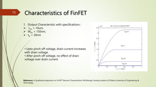
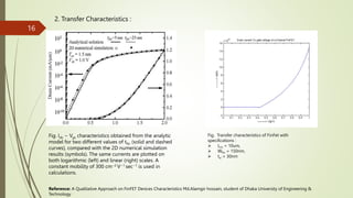
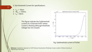
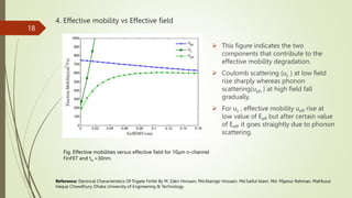
The document discusses FinFET transistors. It provides a history of FinFET development starting in 1998. FinFETs were created to allow Moore's Law to continue by addressing short channel effects in traditional planar MOSFETs as devices continued scaling. FinFETs use a fin-like gate structure to improve gate control and reduce leakage currents. The document outlines FinFET structure, characteristics, fabrication process, advantages, applications and the future of FinFET technology as it aims to scale below 5nm.


![ In 1999, Chenming Hu crammed a record number of
transistors onto a chip with his invention of “FinFET,”
short for Fin Field Effect Transistor.
Invention Of Finfet
1998 – N-channel FinFET (17 nm)
1999 – P-channel FinFET
2001 – 15 nm FinFET
2002 – 10 nm FinFET
2004 – High-κ/metal gate FinFET
Reference: FinFET [Online]. Available: https://en.wikipedia.org/wiki/FinFET
3](https://image.slidesharecdn.com/group1finfetfinal-231111081621-ba332891/85/Group-1_FinFET-Final-pptx-3-320.jpg)
![Moore's law:
the number of transistors on a microchip doubles every two years.
Reference: Moore’s law [Online]. Available: https://en.wikipedia.org/wiki/Moore%27s_law
4](https://image.slidesharecdn.com/group1finfetfinal-231111081621-ba332891/85/Group-1_FinFET-Final-pptx-4-320.jpg)
![Why FinFET?
At a point of scaling MOSFET, short channel effects show up.
Shift of Vth (DIBL)
Sub threshold slope (SS) degrades
Off current (Ioff) Increases
So overall performance degrades.
FinFET is a way to overcome this problem & continue scaling.
Reference: Impact of quantum effects on the short channel effects of III–V nMOSFETs in weak and strong inversion regimes
[Online]. Available: https://www.sciencedirect.com/science/article/abs/pii/S003811011300169X
5](https://image.slidesharecdn.com/group1finfetfinal-231111081621-ba332891/85/Group-1_FinFET-Final-pptx-5-320.jpg)

![Planar MOSFET vs FinFET
• One gate, so less control
over channel
• More leakage current
• Two gates, so more control
over channel
• Very less leakage current
Reference: FinFET Physics [Online]. Available: https://www.mksinst.com/n/finfet-physics
7](https://image.slidesharecdn.com/group1finfetfinal-231111081621-ba332891/85/Group-1_FinFET-Final-pptx-7-320.jpg)
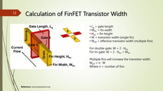
![It is common for a single FinFET transistor to
contain several fins, arranged side by side and
all covered by the same gate, that act
electrically as one, to increase drive strength
and performance.
Reference: A Review Paper on CMOS, SOI and FinFET Technology [Online]. Available: https://www.design-
reuse.com/articles/41330/cmos-soi-finfet-technology-review-paper.html](https://image.slidesharecdn.com/group1finfetfinal-231111081621-ba332891/85/Group-1_FinFET-Final-pptx-8-320.jpg)
![FinFET Classification:
SG FinFET:
• Having 3 Terminals
• Higher Ion & Ioff
• Require lesser area
IG FinFET:
• Having 4 Terminals
• Vth modulation is possible
• Require more area
1. Shorted gate FinFET & Insulated gate FinFET
Reference: FinFETs: From Devices to Architectures [Online]. Available: https://www.hindawi.com/journals/aelc/2014/365689/
9](https://image.slidesharecdn.com/group1finfetfinal-231111081621-ba332891/85/Group-1_FinFET-Final-pptx-9-320.jpg)
![SOI FinFET:
• ∆Hfin ↓
• Expensive
• Lesser Heat Dissipation
Bulk FinFET:
• ∆Hfin↑
• Less Expensive
• Higher Heat Dissipation
• Parasitic BJT
2. SOI FinFET & Bulk FinFET
Reference: Compairing FinFETs: SOI Vs Bulk: Process variability, process cost, and device performance [Online]. Available:
https://www.semanticscholar.org/paper/Compairing-FinFETs%3A-SOI-Vs-Bulk%3A-Process-process-Deshmukh-
Khanzode/8303e7d5bdcc8187b15af29da595f6e33e04a2dd
10](https://image.slidesharecdn.com/group1finfetfinal-231111081621-ba332891/85/Group-1_FinFET-Final-pptx-10-320.jpg)

![Various Gate structures for FET
Tri-gate FinFET
Double-gate
FinFET
Reference: FinFET Evolution [Online]. Available: https://eepower.com/technical-articles/what-is-a-finfet/#
23](https://image.slidesharecdn.com/group1finfetfinal-231111081621-ba332891/85/Group-1_FinFET-Final-pptx-23-320.jpg)


![References
[1] FinFET [Online]. Available: https://en.wikipedia.org/wiki/FinFET
[2] Moore’s law [Online]. Available: https://en.wikipedia.org/wiki/Moore%27s_law
[3] Impact of quantum effects on the short channel effects of III–V nMOSFETs in weak and strong inversion regimes [Online]. Available:
https://www.sciencedirect.com/science/article/abs/pii/S003811011300169X
[4] 1506 Samsung SLSI 14nm FinFET
[5] FinFET Physics [Online]. Available: https://www.mksinst.com/n/finfet-physics
[6] A Review Paper on CMOS, SOI and FinFET Technology [Online]. Available: https://www.design-reuse.com/articles/41330/cmos-soi-finfet-
technology-review-paper.html
[7] FinFETs: From Devices to Architectures [Online]. Available: https://www.hindawi.com/journals/aelc/2014/365689/
[8] Compairing FinFETs: SOI Vs Bulk: Process variability, process cost, and device performance [Online]. Available:
https://www.semanticscholar.org/paper/Compairing-FinFETs%3A-SOI-Vs-Bulk%3A-Process-process-Deshmukh-
Khanzode/8303e7d5bdcc8187b15af29da595f6e33e04a2dd
[9] www.synopsys.com (By Jamil Kawa, R&D Group Director, Synopsys, Inc.)
[10] www.ieeeexplore.org
[11] A Qualitative Approach on FinFET Devices Characteristics Md.Alamgir hossain,student of Dhaka University of Engineering & Technology
[12] Electrical Characteristics Of Trigate Finfet By M. Zakir Hossain, Md.Alamgir Hossain, Md.Saiful Islam, Md. Mijanur Rahman, Mahfuzul Haque
Chowdhury, Dhaka University of Engineering & Technology
[13] https://semiengineering.com/transistor-options-beyond-3nm/
[14] https://sites.ji.sjtu.edu.cn/xinfei-guo/wp-content/uploads/sites/27/2021/05/pdf.pdf
28](https://image.slidesharecdn.com/group1finfetfinal-231111081621-ba332891/85/Group-1_FinFET-Final-pptx-28-320.jpg)