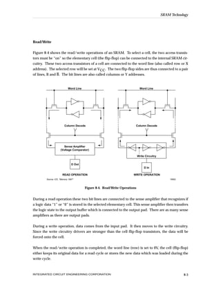
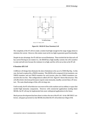
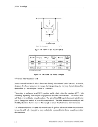
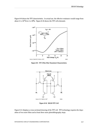
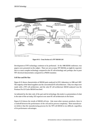
This presentation discusses the basics of Pass Transistor Logic, its advantages, limitation and finally implementation of Boolean functions/Combinational Logic circuits using Pass Transistor Logic.
Designed a fully customized 128x10b SRAM by constructing schematic & virtuoso layout of memory cell array (6T cell), row & column decoder, pre-charge circuit, write circuit and sense amplifier using Cadence. Manually placed and routed all components, performed DRC & LVS debugging of constructed schematic and layout and ran PEX to generate the final Netlist, Hspice Spectre simulation of final design for verification of the correct functionality and analysis of best read, best write cycles & the worst case timing for read and write. Timing and power consumed is analyzed through STA-Primetime (Static timing Analysis)
Implementation of High Reliable 6T SRAM Cell Designiosrjce
Memory can be formed with the integration of large number of basic storing element called cells.
SRAM cell is one of the basic storing unit of volatile semiconductor memory that stores binary logic '1' or '0' bit.
Modified read and write circuits were proposed in this paper to address incorrect read and write operations in
conventional 6T SRAM cell design available in open literature. Design of a new highly reliable 6T SRAM cell
design is proposed with reliable read, write operations and negative bit line voltage (NBLV). Simulations are
carried out using MENTOR GRAPHICS
I have prepared it to create an understanding of delay modeling in VLSI.
Regards,
Vishal Sharma
Doctoral Research Scholar,
IIT Indore
vishalfzd@gmail.com
In the project#1, IBM 130nm process is used to design and manual layout a 128 word SRAM, with word size 10bits. Cadence's Virtuoso is applied for layout editing, DRC and LVS running and circuit simulation.
This presentation has given a brief introduction and working of CMOS Logic Structures which includes MOS logic, CMOS logic, CMOS logic structure, CMOS complementary logic, pass transistor logic, bi CMOS logic, pseudo –nMOS logic, CMOS domino logic, Cascode Voltage Switch Logic(CVSL), clocked CMOS logic(c²mos), dynamic CMOS logic
Analysis and Simulation of Sub-threshold Leakage Current in P3 SRAM Cell at D...IDES Editor
In this work, the analysis and simulation work is
proposed for the low-power (reduced subthreshold leakage)
and high performance SRAM bit-cells for mobile multimedia
applications in deep-sub-micron (DSM) CMOS technology.
The sub-threshold leakage analysis of the P3 SRAM cell has
been carried out. It has been observed that due to pMOS
stacking and full supply body-biasing, there is a reduction of
70% and 86% in sub-threshold leakage current at VDD=0.8V
and VDD=0.7V respectively as compared to conventional 6T
SRAM cell. Due to this a reduction in the standby power has
been achieved w.r.t the 6T and PP SRAM design at a bearable
expense of the SVNM and the WTV.
Deep submicron-backdoors-ortega-syscan-2014-slidesortegaalfredo
Malicious hardware is a mature topic but previous research has focused almost exclusively on theoretical applications. In this article, practical implementations of gate-level backdoors will be presented using the Verilog hardware description language, then simulated and finally synthesized using freely available deep sub-micron (45-180 nm) standard cells, resulting in a backdoored latest-generation ARM CPU, suitable for fabrication and massive deployment.
Analysis of FinFET based Low Power SRAM Cellijsrd.com
As CMOS electronic devices are continuously shrinking to nanometer regime, leads to increasing the consequences of short channel effects and variability due to the process parameters which lead to cause the reliability of the circuit as well as performance. To solve these issues of CMOS, FINFET is one of the promising and better technologies without sacrificing reliability and performance for its applications and the circuit design. Among the various embedded memory technologies, SRAM provides the highest performance along with low standby power consumption. In CMOS circuits, high leakage current in deep-submicron regimes is becoming a significant contributor to power dissipation due to reduction in threshold voltage, channel length, and gate oxide thickness. FinFET based SRAM design can be used as an alternative solution to the bulk devices. FinFET is suitable for Nano scale memory circuits design due to its reduced Short Channel Effects (SCE) and leakage current. As the impact of process variations become increasingly significant in ultra deep submicron technologies, FinFETs are becoming increasingly popular a contender for replacement of bulk FETs due to favorable device characteristics. The paper focuses on study of various design aspects of FinFET based SRAM.
250nm Technology Based Low Power SRAM Memoryiosrjce
High integration density, low power and fastperformance are all critical parameters in designing of
memory blocks. Static Random Access Memories (SRAMs)’s focusing on optimizing dynamic power concept of
virtual source transistors is used for removing direct connection between VDD and GND.
Also stacking effect can be reduced by switching off the stacktransistors when the memory is ideal and the
leakage current using SVL techniques This paper discusses the evolution of 9t SRAM circuits in terms of low
power consumption, The whole circuit verification is done on the Tanner tool, Schematic of the
SRAM cell is designed on the S-Edit and net list simulation done by using T-spice and waveforms are analyzed
through the W-edit
A Novel Low Power Energy Efficient SRAM Cell With Reduced Power Consumption u...iosrjce
In modern high performance integrated circuits, maximum of the total active mode energy is
consumed due to leakage current. SRAM cell array is main source of leakage current since majority of
transistor are utilized for on-chip memory in today high performance microprocessor and system on chip
designs. Therefore the design of low leakage SRAM is required. Reducing power dissipation, supply voltage,
leakage currents, area of chip are the most important parameters in today`s VLSI designs. But scaling of these
parameters will lead to drastic increase in sub threshold leakage currents and power dissipation because of that
performance of the design is degraded. So to overcome these issues it is better to concentrate on reduction of
active leakage currents and dynamic power dissipation by using power reduction techniques. In this paper 9T
SRAM (data retention p-gated) cell for low voltage and energy constrain application is analyzed with respect to
power dissipation, area and delay. The analyzed design of 9T SRAM cell with MTCMOS technique has been
proposed. Designed circuits are simulated in Microwind 3.1 VLSI CAD Tool in 90 and 65nm CMOS technology.
Implementation of an Efficient SRAM for Ultra-Low Voltage Application Based o...IOSR Journals
Abstract: Operation of standard 6T static random access memory (SRAM) cells at sub or near threshold
voltages is unfeasible, predominantly due to degraded static noise margins (SNM) and poor robustness. We
analyze Schmitt-Trigger (ST)-based differential-sensing static random access memory (SRAM) bitcells for
ultralow-voltage operation. The ST-based SRAM bitcells address the fundamental conflicting design
requirement of the read versus write operation of a conventional 6T bitcell. The ST operation gives better readstability
as well as better write-ability compared to the standard 6T bitcell. In this paper we are going to
propose a new SRAM bitcell for the purpose of read stability and write ability by using 90nm technology , and
less power consumption, less area than the existing Schmitt trigger1 based SRAM. Design and simulations were done using DSCH and Microwind.
Index Terms: read stability, write ability, Schmitt trigger.
Using CMOS Sub-Micron Technology VLSI Implementation of Low Power, High Speed...VLSICS Design
Abstract This paper deals with the design and analysis of high speed Static Random Access Memory (SRAM) cell and Dynamic Random Access Memory (DRAM) cell to develop low power consumption. SRAM and DRAM cells have been the predominant technologies used to implement memory cells in computer systems, each one having its advantages and shortcomings. SRAM cells are faster and require no refresh since reads are not destructive. In contrast, DRAM cells provide higher density and minimal leakage energy. Here we use 12-transistor SRAM cell built from a simple static latch and tri state inverter. The reading action itself refreshes the content of memory. The SRAM access path is split into two portions: from address input to word line rise (the row decoder) and from word line rise to data output (the read data path). The decoder which constitutes the path from address input to the word line rise is implemented as a binary structure by implementing a multi-stage path. The key to low power operation in the SRAM data path is to reduce the signal swings on the high capacitance nodes like the bit lines and the data lines.
Using CMOS Sub-Micron Technology VLSI Implementation of Low Power, High Spee...VLSICS Design
This paper deals with the design and analysis of high speed Static Random Access Memory (SRAM) cell and Dynamic Random Access Memory (DRAM) cell to develop low power consumption. SRAM and DRAM cells have been the predominant technologies used to implement memory cells in computer systems, each one having its advantages and shortcomings. SRAM cells are faster and require no refresh since reads are not destructive. In contrast, DRAM cells provide higher density and minimal leakage energy. Here we use 12-transistor SRAM cell built from a simple static latch and tri state inverter. The reading action itself refreshes the content of memory. The SRAM access path is split into two portions: from address input to word line rise (the row decoder) and from word line rise to data output (the read data path). The decoder which constitutes the path from address input to the word line rise is implemented as a binary structure by implementing a multi-stage path. The key to low power operation in the SRAM data path is to reduce the signal swings on the high capacitance nodes like the bit lines and the data lines.
RAM(Random Access memory) is a volatile memory.RAM is our working memory storage. All the data, which the PC uses and works with during operation, are stored here. Data are stored on drives, typically the hard drive. However, for the CPU to work with those data, they must be read into the working memory storage, which is made up of RAM chips.
Historical review:
Back in the 80's, PC's were equipped with RAM in quantities of 64 KB, 256 KB, 512 KB and finally 1 MB. Around 1990, advanced operating systems, like Windows, appeared on the market, that started the RAM race. The PC needed more and more RAM. That worked fine with the 386 processor, which could address larger amount of RAM. The first Windows operated PC's could address 2 MB RAM, but 4 MB soon became the standard. The race has continued through the 90's, as RAM prices have dropped dramatically. Today it would be foolish to consider less than 64 MB RAM in a PC. The OS like windows Xp requires better than this.
Building Your Employer Brand with Social MediaLuanWise
Presented at The Global HR Summit, 6th June 2024
In this keynote, Luan Wise will provide invaluable insights to elevate your employer brand on social media platforms including LinkedIn, Facebook, Instagram, X (formerly Twitter) and TikTok. You'll learn how compelling content can authentically showcase your company culture, values, and employee experiences to support your talent acquisition and retention objectives. Additionally, you'll understand the power of employee advocacy to amplify reach and engagement – helping to position your organization as an employer of choice in today's competitive talent landscape.
B2B payments are rapidly changing. Find out the 5 key questions you need to be asking yourself to be sure you are mastering B2B payments today. Learn more at www.BlueSnap.com.
Anny Serafina Love - Letter of Recommendation by Kellen Harkins, MS.AnnySerafinaLove
This letter, written by Kellen Harkins, Course Director at Full Sail University, commends Anny Love's exemplary performance in the Video Sharing Platforms class. It highlights her dedication, willingness to challenge herself, and exceptional skills in production, editing, and marketing across various video platforms like YouTube, TikTok, and Instagram.
Event Report - SAP Sapphire 2024 Orlando - lots of innovation and old challengesHolger Mueller
Holger Mueller of Constellation Research shares his key takeaways from SAP's Sapphire confernece, held in Orlando, June 3rd till 5th 2024, in the Orange Convention Center.
At Techbox Square, in Singapore, we're not just creative web designers and developers, we're the driving force behind your brand identity. Contact us today.
In the Adani-Hindenburg case, what is SEBI investigating.pptxAdani case
Adani SEBI investigation revealed that the latter had sought information from five foreign jurisdictions concerning the holdings of the firm’s foreign portfolio investors (FPIs) in relation to the alleged violations of the MPS Regulations. Nevertheless, the economic interest of the twelve FPIs based in tax haven jurisdictions still needs to be determined. The Adani Group firms classed these FPIs as public shareholders. According to Hindenburg, FPIs were used to get around regulatory standards.
Premium MEAN Stack Development Solutions for Modern BusinessesSynapseIndia
Stay ahead of the curve with our premium MEAN Stack Development Solutions. Our expert developers utilize MongoDB, Express.js, AngularJS, and Node.js to create modern and responsive web applications. Trust us for cutting-edge solutions that drive your business growth and success.
Know more: https://www.synapseindia.com/technology/mean-stack-development-company.html
Navigating the world of forex trading can be challenging, especially for beginners. To help you make an informed decision, we have comprehensively compared the best forex brokers in India for 2024. This article, reviewed by Top Forex Brokers Review, will cover featured award winners, the best forex brokers, featured offers, the best copy trading platforms, the best forex brokers for beginners, the best MetaTrader brokers, and recently updated reviews. We will focus on FP Markets, Black Bull, EightCap, IC Markets, and Octa.
FIA officials brutally tortured innocent and snatched 200 Bitcoins of worth 4...jamalseoexpert1978
Farman Ayaz Khattak and Ehtesham Matloob are government officials in CTW Counter terrorism wing Islamabad, in Federal Investigation Agency FIA Headquarters. CTW and FIA kidnapped crypto currency owner from Islamabad and snatched 200 Bitcoins those worth of 4 billion rupees in Pakistan currency. There is not Cryptocurrency Regulations in Pakistan & CTW is official dacoit and stealing digital assets from the innocent crypto holders and making fake cases of terrorism to keep them silent.
3.0 Project 2_ Developing My Brand Identity Kit.pptxtanyjahb
A personal brand exploration presentation summarizes an individual's unique qualities and goals, covering strengths, values, passions, and target audience. It helps individuals understand what makes them stand out, their desired image, and how they aim to achieve it.
3.0 Project 2_ Developing My Brand Identity Kit.pptx
Sram technology
1. 8 SRAM TECHNOLOGY
OVERVIEW
An SRAM (Static Random Access Memory) is designed to fill two needs: to provide a direct
interface with the CPU at speeds not attainable by DRAMs and to replace DRAMs in systems
that require very low power consumption. In the first role, the SRAM serves as cache memory,
interfacing between DRAMs and the CPU. Figure 8-1 shows a typical PC microprocessor
memory configuration.
SRAM DRAM
External Cache (L2) Main Memory
64KB to 1MB 4MB to 512MB
Microprocessor
Internal Cache (L1)
8KB to 32KB
Source: Micron/ICE, "Memory 1997" 20812
Figure 8-1. Typical PC Microprocessor Memory Configuration
The second driving force for SRAM technology is low power applications. In this case, SRAMs
are used in most portable equipment because the DRAM refresh current is several orders of mag-
nitude more than the low-power SRAM standby current. For low-power SRAMs, access time is
comparable to a standard DRAM. Figure 8-2 shows a partial list of Hitachi’s SRAM products and
gives an overview of some of the applications where these SRAMs are found.
HOW THE DEVICE WORKS
The SRAM cell consists of a bi-stable flip-flop connected to the internal circuitry by two access
transistors (Figure 8-3). When the cell is not addressed, the two access transistors are closed and
the data is kept to a stable state, latched within the flip-flop.
INTEGRATED CIRCUIT ENGINEERING CORPORATION 8-1
2. SRAM Technology
100 Industrial/Peripheral Buffer Memory
64Kbit Low-Power SRAM
256Kbit 1Mbit 512K x 8
Low-Power SRAM Low-Power SRAM Low-Power SRAM
50
Mass Storage Buffer Memory
32K x 8 1M x 4/512K x 8
Asynchronous SRAM 128K x 8/64K x 16 Asynchronous SRAM
Access Time (ns)
20
Asynchronous SRAM
10 32K x 32/32K x 36
PC Cache Memory Asynchronous SRAM
256K x 18/128K x 36
5 32K x 36 LVCMOS SSRAM
LVCMOS/HSTL SSRAM
Non PC Cache Memory
2
64Kbit 256Kbit 1Mbit 4Mbit
Device Density
Source: Hitachi/ICE, "Memory 1997" 22607
Figure 8-2. Hitachi’s SRAM Products
Word Line
B B
To Sense Amplifier
Source: ICE, "Memory 1997" 20019
Figure 8-3. SRAM Cell
The flip-flop needs the power supply to keep the information. The data in an SRAM cell is volatile
(i.e., the data is lost when the power is removed). However, the data does not “leak away” like in
a DRAM, so the SRAM does not require a refresh cycle.
8-2 INTEGRATED CIRCUIT ENGINEERING CORPORATION
3. SRAM Technology
Read/Write
Figure 8-4 shows the read/write operations of an SRAM. To select a cell, the two access transis-
tors must be “on” so the elementary cell (the flip-flop) can be connected to the internal SRAM cir-
cuitry. These two access transistors of a cell are connected to the word line (also called row or X
address). The selected row will be set at VCC. The two flip-flop sides are thus connected to a pair
of lines, B and B. The bit lines are also called columns or Y addresses.
Word Line Word Line
Column Decode Column Decode
Sense Amplifier
(Voltage Comparator)
Write Circuitry
D Out
D In
READ OPERATION WRITE OPERATION
Source: ICE, "Memory 1997" 19952
Figure 8-4. Read/Write Operations
During a read operation these two bit lines are connected to the sense amplifier that recognizes if
a logic data “1” or “0” is stored in the selected elementary cell. This sense amplifier then transfers
the logic state to the output buffer which is connected to the output pad. There are as many sense
amplifiers as there are output pads.
During a write operation, data comes from the input pad. It then moves to the write circuitry.
Since the write circuitry drivers are stronger than the cell flip-flop transistors, the data will be
forced onto the cell.
When the read/write operation is completed, the word line (row) is set to 0V, the cell (flip-flop)
either keeps its original data for a read cycle or stores the new data which was loaded during the
write cycle.
INTEGRATED CIRCUIT ENGINEERING CORPORATION 8-3
4. SRAM Technology
Data Retention
To work properly and to ensure that the data in the elementary cell will not be altered, the SRAM
must be supplied by a VCC (power supply) that will not fluctuate beyond plus or minus five or
ten percent of the VCC.
If the elementary cell is not disturbed, a lower voltage (2 volts) is acceptable to ensure that the cell
will correctly keep the data. In that case, the SRAM is set to a retention mode where the power
supply is lowered, and the part is no longer accessible. Figure 8-5 shows an example of how the
VCC power supply must be lowered to ensure good data retention.
,,,,
Data Retention Mode
3.0V VDR ≥ 2V 3.0V
VCC
tCDR tR
,,,,
,
,
,
CE
Source: Cypress/ICE, "Memory 1997" 22460
Figure 8-5. SRAM Data Retention Waveform
MEMORY CELL
Different types of SRAM cells are based on the type of load used in the elementary inverter of the
flip-flop cell. There are currently three types of SRAM memory cells :
• The 4T cell (four NMOS transistors plus two poly load resistors)
• The 6T cell (six transistors—four NMOS transistors plus two PMOS transistors)
• The TFT cell (four NMOS transistors plus two loads called TFTs)
4 Transistor (4T ) Cell
The most common SRAM cell consists of four NMOS transistors plus two poly-load resistors
(Figure 8-6). This design is called the 4T cell SRAM. Two NMOS transistors are pass-transistors.
These transistors have their gates tied to the word line and connect the cell to the columns. The
two other NMOS transistors are the pull-downs of the flip-flop inverters. The loads of the invert-
ers consist of a very high polysilicon resistor.
This design is the most popular because of its size compared to a 6T cell. The cell needs room only
for the four NMOS transistors. The poly loads are stacked above these transistors. Although the
4T SRAM cell may be smaller than the 6T cell, it is still about four times as large as the cell of a
comparable generation DRAM cell.
8-4 INTEGRATED CIRCUIT ENGINEERING CORPORATION
5. SRAM Technology
W
+V
B B
To Sense Amps
Source: ICE, "Memory 1997" 18470A
Figure 8-6. SRAM 4T (Four-Transistor) Cell
The complexity of the 4T cell is to make a resistor load high enough (in the range of giga-ohms) to
minimize the current. However, this resistor must not be too high to guarantee good functionality.
Despite its size advantage, the 4T cells have several limitations. These include the fact that each cell
has current flowing in one resistor (i.e., the SRAM has a high standby current), the cell is sensitive
to noise and soft error because the resistance is so high, and the cell is not as fast as the 6T cell.
6 Transistor (6T) Cell
A different cell design that eliminates the above limitations is the use of a CMOS flip-flop. In this
case, the load is replaced by a PMOS transistor. This SRAM cell is composed of six transistors, one
NMOS transistor and one PMOS transistor for each inverter, plus two NMOS transistors con-
nected to the row line. This configuration is called a 6T Cell. Figure 8-7 shows this structure. This
cell offers better electrical performances (speed, noise immunity, standby current) than a 4T struc-
ture. The main disadvantage of this cell is its large size.
Until recently, the 6T cell architecture was reserved for niche markets such as military or space that
needed high immunity components. However, with commercial applications needing faster
SRAMs, the 6T cell may be implemented into more widespread applications in the future.
Much process development has been done to reduce the size of the 6T cell. At the 1997 ISSCC con-
ference, all papers presented on fast SRAMs described the 6T cell architecture (Figure 8-8).
INTEGRATED CIRCUIT ENGINEERING CORPORATION 8-5
6. SRAM Technology
W
+V
B B
To Sense Amps
Source: ICE , "Memory 1997" 18471A
Figure 8-7. SRAM 6T (Six Transistor) Cell
Cell Size Die Size
Density Company Cell Type Process
(µm2) (mm2)
4Mbit NEC 6T 12.77 0.25µm 132
4Mbit IBM 6T 18.77 0.3µm 145
0.2µm Leff
128Kbit Hitachi 6T 21.67 0.35µm 5.34
Source: ICE, "Memory 1997" 22459
Figure 8-8. 1997 ISSCC Fast SRAM Examples
TFT (Thin Film Transistor) Cell
Manufacturers have tried to reduce the current flowing in the resistor load of a 4T cell. As a result,
designers developed a structure to change, during operating, the electrical characteristics of the
resistor load by controlling the channel of a transistor.
This resistor is configured as a PMOS transistor and is called a thin film transistor (TFT). It is
formed by depositing several layers of polysilicon above the silicon surface. The source/chan-
nel/drain is formed in the polysilicon load. The gate of this TFT is polysilicon and is tied to the
gate of the opposite inverter as in the 6T cell architecture. The oxide between this control gate and
the TFT polysilicon channel must be thin enough to ensure the effectiveness of the transistor.
The performance of the TFT PMOS transistor is not as good as a standard PMOS silicon transis-
tor used in a 6T cell. It should be more realistically compared to the linear polysilicon resistor
characteristics.
8-6 INTEGRATED CIRCUIT ENGINEERING CORPORATION
7. SRAM Technology
Figure 8-9 shows the TFT characteristics. In actual use, the effective resistance would range from
about 11 x 1013Ω to 5 x 10⁹Ω. Figure 8-10 shows the TFT cell schematic.
–10–6
Vd = –4V
–10–8
Drain Current, Id (A)
Vg
–10–10
Tox = 25nm
Tpoly = 38nm
–10–12
L/W = 1.6/0.6µm
2 0 –2 –4 –6 –8
Gate Voltage, Vg (V)
Source: Hitachi/ICE, Memory 1997" 19953
Figure 8-9. TFT (Thin Film Transistor) Characteristics
Word Line
Poly-Si
PMOS
BL BL
Source: ICE, "Memory 1997" 19954
Figure 8-10. SRAM TFT Cell
Figure 8-11 displays a cross-sectional drawing of the TFT cell. TFT technology requires the depo-
sition of two more films and at least three more photolithography steps.
INTEGRATED CIRCUIT ENGINEERING CORPORATION 8-7
8. SRAM Technology
1st Metal (BIT Line)
,,,,,,
,,,,,,
,,,,,,
3rd Poly-Si 4th Poly-Si
,,,,,,,,,,, 2nd Poly-Si
,,,,,, (Gate Electrode
,,,,,,,,,,,
,,,,,,,,,,,
(Channel of TFT)
,,,,,
,,,,,,,,,,
,,,,,,,,,,
(Internal Connection) Contact
,,,,,,,,
,,,,,, of TFT) ,,,,,
,,,,,,,,,,, ,,,,,,,,,,
,,,,,,,,,,
(W-Plug)
,,,,,
,,,,,,,,
,,,,,,,, ,,,,,,,,,,
,,,,,,,,,,
2nd Direct
Contact
,,,,,,,,,, ,,,,,,, ,,,,,, ,,,,,,,,,,
,,,,,,,,
,,,,,,,,,,,,,
,,,,,,,,,, ,,,,,,, ,,,,,, ,,,,,,,,,,
,,,,,,,,
,,,,,,,,,,,,, ,,,,,,,,,,,,,,,
,,,, ,,,,,,,,
,,,,,,,,,,,,, ,,,,,,,,,,,,,,,
,,,, ,,,,,,, ,,,,,, ,,,,,,,,,,
Isolation
N+ N+ N+ N+
Access
N+ Diffusion TiSi2
Driver Transistor
Region 1st Poly-Si
Transistor
(GND Line) (Gate Electrode
of Bulk Transistor)
Source: IEDM 91/ICE, "Memory 1997" 18749
Figure 8-11. Cross Section of a TFT SRAM Cell
Development of TFT technology continues to be performed. At the 1996 IEDM conference, two
papers were presented on the subject. There are not as many TFT SRAMs as might be expected,
due to a more complex technology compared to the 4T cell technology and, perhaps, due to poor
TFT electrical characteristics compared to a PMOS transistor.
Cell Size and Die Size
Figure 8-12 shows characteristics of SRAM parts analyzed in ICE’s laboratory in 1996 and 1997.
The majority of the listed suppliers use the conventional 4T cell architecture. Only two chips were
made with a TFT cell architecture, and the only 6T cell architecture SRAM analyzed was the
Pentium Pro L2 Cache SRAM from Intel.
As indicated by the date code of the part and its technology, this study is a presentation of what
is the state-of-the-art today. ICE expects to see more 6T cell architectures in the future.
Figure 8-13 shows the trends of SRAM cell size. Like most other memory products, there is
a tradeoff between the performance of the cell and its process complexity. Most manufactur-
ers believe that the manufacturing process for the TFT-cell SRAM is too difficult, regardless
of its performance advantages.
8-8 INTEGRATED CIRCUIT ENGINEERING CORPORATION
9. SRAM Technology
Cell Size Die Size Min Gate (N)
Date Code Cell Type
(µm2) (mm2) (µm)
Toshiba 9509 4T 22 144 0.65
4Mbit
Samsung 1995 4T 14.25 33 0.5
1Mbit
Galvantech 9524 4T 16.5 31 0.4
1Mbit
Hitachi 9539 4T 19 64 0.45
1Mbit
NEC 9436 4T 19 67 0.6
1Mbit
Motorola 9443 4T 40 108 0.6
1Mbit
Hualon 9523 4T 30 13.5 0.45
256Kbit
ISSI 9445 4T 27.5 50 0.5
1Mbit
Mosel-Vitelic 9409 4T 44 94.7 0.65
1Mbit
NEC 9506 4T 15.7 42.5 0.5
1Mbit
Samsung 9606 TFT 11.7 77.8 0.65
4Mbit
Sony ? TFT 20 59 0.5
1Mbit
TM Tech 9530 4T 20 35 0.35
1Mbit
UMC 9631 4T 11.25 41 0.3
2Mbit
Winbond 9612 4T 10.15 32.5 0.5
1Mbit
Intel — 6T 33 — 0.35
Pentium Pro
L2 Cache
Source: ICE, "Memory 1997" 22461
Figure 8-12. Physical Geometries of SRAMs
Figures 8-14 and 8-15 show size and layout comparisons of a 4T cell and a 6T cell using the same technol-
ogy generation (0.3µm process). These two parts were analyzed by ICE’s laboratory in 1996.
One of the major process improvements in the development of SRAM technology is the so called
self aligned contact (SAC). This process suppresses the spacing between the metal contacts and
the poly gates and is illustrated in Figure 8-16.
INTEGRATED CIRCUIT ENGINEERING CORPORATION 8-9
10. SRAM Technology
1,000
100
Cell Size (µm2)
6T Cell
10
4T (and TFT) Cell
1
1 Micron 0.8 Micron 0.5-0.6 Micron 0.35 Micron 0.25 Micron
Technology
Source: ICE, "Memory 1997" 19989A
Figure 8-13. Trend of SRAM Cell Sizes
CONFIGURATION
As shown in Figure 8-17, SRAMs can be classified in four main categories. The segments are asyn-
chronous SRAMs, synchronous SRAMs, special SRAMs, and non-volatile SRAMs. These are
highlighted below.
Asynchronous SRAMs
Figure 8-18 shows a typical functional block diagram and a typical pin configuration of an asyn-
chronous SRAM. The memory is managed by three control signals. One signal is the chip select
(CS) or chip enable (CE) that selects or de-selects the chip. When the chip is de-selected, the part
is in stand-by mode (minimum current consumption) and the outputs are in a high impedance
state. Another signal is the output enable (OE) that controls the outputs (valid data or high
impedance). Thirdly, is the write enable (WE) that selects read or write cycles.
Synchronous SRAMs
As computer system clocks increased, the demand for very fast SRAMs necessitated variations on
the standard asynchronous fast SRAM. The result was the synchronous SRAM (SSRAM).
8-10 INTEGRATED CIRCUIT ENGINEERING CORPORATION