DRAM CELL
Read and Write Operations, Working
Naman Bhalla
Amber Bhargava
What is a DRAM ?
• A type of random access semiconductor
memory that stores each bit of data in a
separate tiny capacitor within an integrated
circuit.
• The capacitor can either be charged or
discharged (1 or 0).
• Volatile memory - Loses data quickly when
power is removed. (Limited Data Remanence)
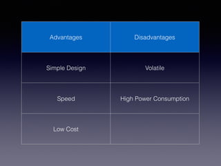
Advantages Disadvantages
Simple Design Volatile
Speed High Power Consumption
Low Cost
Types of DRAM
Based on Interface for Communication
• Fast Page Mode (FPM) DRAM
• Extended Data Out (EDO) DRAM
• Synchronous (S) DRAM
• Single Data Rate SDRAM
• Double Data Rate (DDR) SDRAM
• DDR2, DDR3, ……
Synchronous DRAM
• Types of DRAM synchronised
with the clock speed of the
microprocessor.
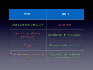
DRAM SRAM
Less expensive to produce. Expensive.
Needs to be refreshed
periodically.
Doesn’t need to be refreshed.
Slower Faster in reads and writes.
Consumes less power in active
state.
Consumes considerably less
power in sleep mode.
Why called “DRAM” ?
• The electric charge on the capacitors slowly leaks
off.
• Without intervention the data on the chip would
soon be lost.
• DRAM requires an external memory refresh circuit
which periodically rewrites the data in the
capacitors, restoring them to their original charge.
• Thus, it is “DYNAMIC” !!
DRAM Cell Design
• A capacitor to store each bit of data.
• A transfer device that acts as a switch.
• The presence of charge in the capacitor
indicates a logic "1" and the absence of
charge indicates a logical “0".
• Two lines are connected to each dynamic
RAM cell - the Word Line (W/L) and the Bit
Line (B/L) connect as shown so that the
required cell within a matrix can have data
read or written to it.
• To improve the write or read capabilities and
speed, the overall dynamic RAM memory may
be split into sub-arrays.
• The presence of multiple sub-arrays shortens
the word and bit lines and this reduces the time
to access the individual cells.
• For example a 256 Mbit dynamic RAM, DRAM
may be split into 16 smaller 16Mbit arrays.
Read and Write
Operations
There are several lines that are used in the
read and write operations
RAS - Row Address Strobe
• As the name implies, the /RAS line strobes the
row to be addressed.
• The address inputs are captured on the falling
edge of the /RAS line.
• The row is held open as long as /RAS remains
low.
CAS - Column Address
Strobe
• This line selects the column to be addressed.
• The address inputs are captured on the falling
edge of /CAS.
• It enables a column to be selected from the
open row for read or write operations.
WE - Write Enable
• This signal determines whether a given falling
edge of /CAS is a read or write.
• Low enables the write action, while high enables
a read action.
• If low (write), the data inputs are also captured
on the falling edge of /CAS.
OE - Output Enable
• The /OE signal is typically used when controlling
multiple memory chips in parallel.
• It controls the output to the data I/O pins.
• The data pins are driven by the DRAM chip if /
RAS and /CAS are low, /WE is high, and /OE is
low.
• In many applications, /OE can be permanently
connected low.
DRAM Read
Step 1 …
• Initially, both RAS* and CAS* are high.
Step 2 …
• A valid row address is applied to the
address pins of the DRAM
• RAS goes low.
• The row address is latched into the row
address buffer on the falling edge of RAS*
and decoded.
Step 3 …
• The decoded row address is applied to a
row line driver.
• This forces one word line to high, thus
connecting a row of DRAM cells.
Step 4 …
• Sensing occurs.
• Sensing is essentially the amplification of
the differential voltage between the two digit
lines.
• The P sense amplifier and the N sense
amplifier are generally fired sequentially.
• First, the N sense amplifier is fired by
bringing NLAT* (N sense-amplifier latch)
toward ground.
• As the voltage difference between NLAT
and the digit lines increases, the NMOS
transistor whose gate is connected to the
higher voltage digit line begins to conduct.
Step 4 (continued) …
• Conduction causes the low-voltage digit line
to be brought to discharge towards NLAT*
and finally to be brought to ground voltage.
• The other NMOS transistor will not conduct.
• As the low-voltage digit line is close to
ground, the corresponding PMOS transistor
is driven into conduction.
• As a result of this operation, all digit lines
are either driven to high or to low according
to the contents of the DRAM cell in the row.
Step 5 …
• The column address has been strobed
into the column address buffer in the
meantime.
• When CAS* falls, the column address is
decoded and one of the sense
amplifiers is connected to the data out
buffer.
Step 6 …
• When RAS* is de-asserted, the word
line goes to low
• All DRAM cells in the row are now
disconnected from the digit line.
DRAM Write
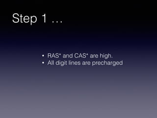
Step 1 …
• RAS* and CAS* are high.
• All digit lines are precharged
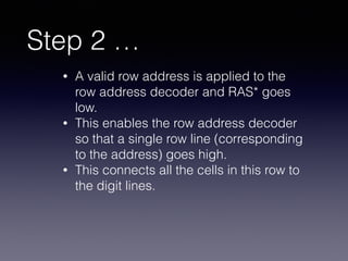
Step 2 …
• A valid row address is applied to the
row address decoder and RAS* goes
low.
• This enables the row address decoder
so that a single row line (corresponding
to the address) goes high.
• This connects all the cells in this row to
the digit lines.
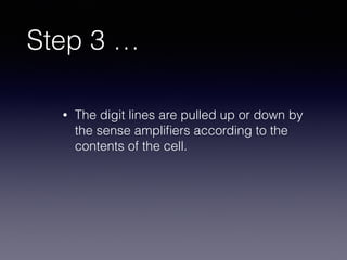
Step 3 …
• The digit lines are pulled up or down by
the sense amplifiers according to the
contents of the cell.
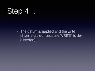
Step 4 …
• The datum is applied and the write
driver enabled (because WRITE* is de-
asserted).
Step 5 …
• A valid column address is applied to the
column address decoder and CAS*
goes low.
• The write driver overdrives the sense
amplifier selected by the column
address decoder.
Step 6 …
• RAS* and CAS* go high again.
• The row line goes low and all cells are
now disconnected from the digit lines.
WORKING
• DRAM Refresh
• Banking
• Pipelining
• Prefetching
DRAM Refresh
DRAM Refresh …
• The capacitor in each DRAM cell discharges slowly.
• At certain intervals, we need to recharge the DRAM cell.
• This is achieved by reading the cell.
• The read will place the contents of the cell on the digit
line, which is then pulled up to full level by the sense
amplifiers.
• When the word line is de-asserted, all cells in the row
have their contents restored at full charge / discharge
level.
“A refresh operation thus refreshes all the
cells in the same row at once!”
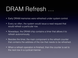
DRAM Refresh …
• Early DRAM memories were refreshed under system control.
• Every so often, the system would issue a read request that
would refresh a particular row.
• Nowadays, the DRAM chip contains a timer that allows it to
refresh autonomously.
• Besides the timer, the main component is the refresh counter
that contains the address of the row that needs to be refreshed.
• When a refresh operation is finished, then the counter is set to
the next row in a cyclical manner.
“The need to refresh amounts to using a
certain (small) portion of the DRAM
bandwidth.”
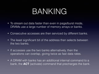
BANKING
• To stream out data faster than even in page/burst mode,
DRAMs use a large number of memory arrays or banks.
• Consecutive accesses are then serviced by different banks.
• The least significant bit of the address then selects between
the two banks.
• If accesses use the two banks alternatively, then the
operations can overlap, giving twice as fast data rates.
• A DRAM with banks has an additional internal command to a
bank, the ACT (activate) command that precharges the bank.
PIPELINING
• By pipelining the addresses, the average access
time can be sped up.
• In this case, the input latch is used to store the
incoming address, while the DRAM is still working
on the previous command.
• The pipeline has three stages, the first for the
input (address and possibly data), the second for
the bank access, and the third for latching the
output (for a read).
PREFETCHING
• We can increase the speed of a synchronous
DRAM by prefetching.
• In this case more than one data word is fetched
from the memory on each address cycle and
transferred to a data selector on the output
buffer.
• Multiple words of data can then be sequentially
clocked out for each memory address.
THANKS !!