Downloaded 246 times

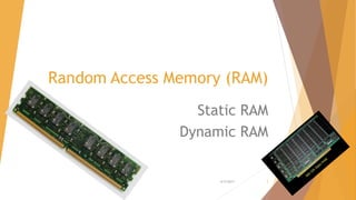
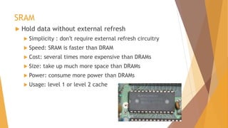
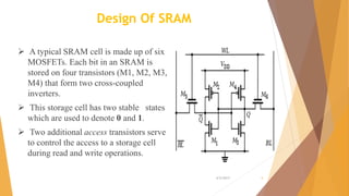


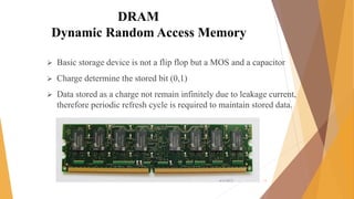

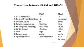


This document is a presentation on RAM that was presented by Tipu Sultan and Md Shakhawat Hossain Sujon to Tafisr Ahmed Khan. It summarizes the key differences between SRAM and DRAM. SRAM does not require refresh cycles but is more expensive and slower than DRAM. A typical SRAM cell uses 6 transistors arranged in two cross-coupled inverters, while a DRAM cell uses one transistor and one capacitor. DRAM must perform periodic refresh cycles to maintain its data due to capacitor leakage, whereas SRAM maintains its data statically without refresh.