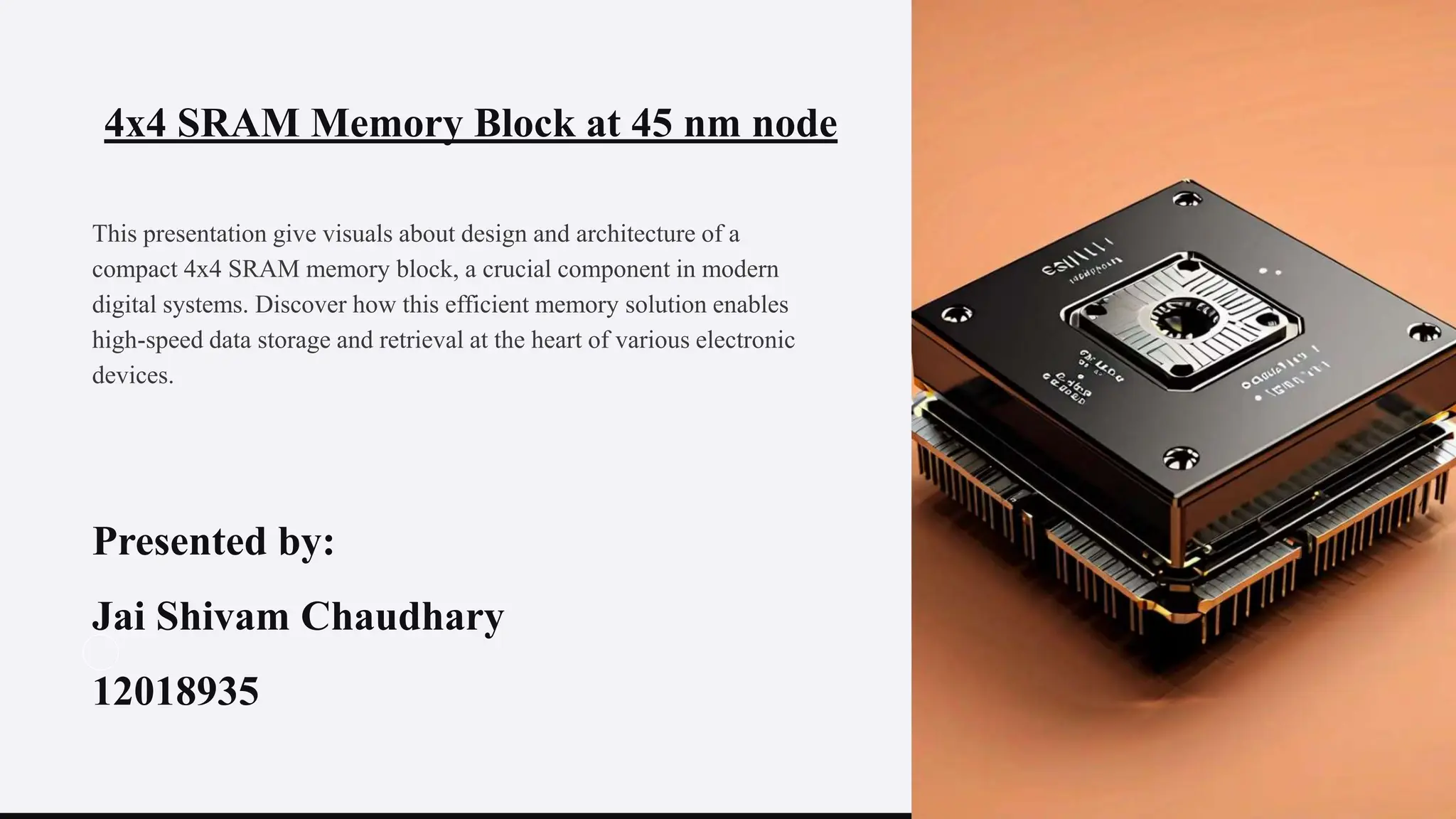
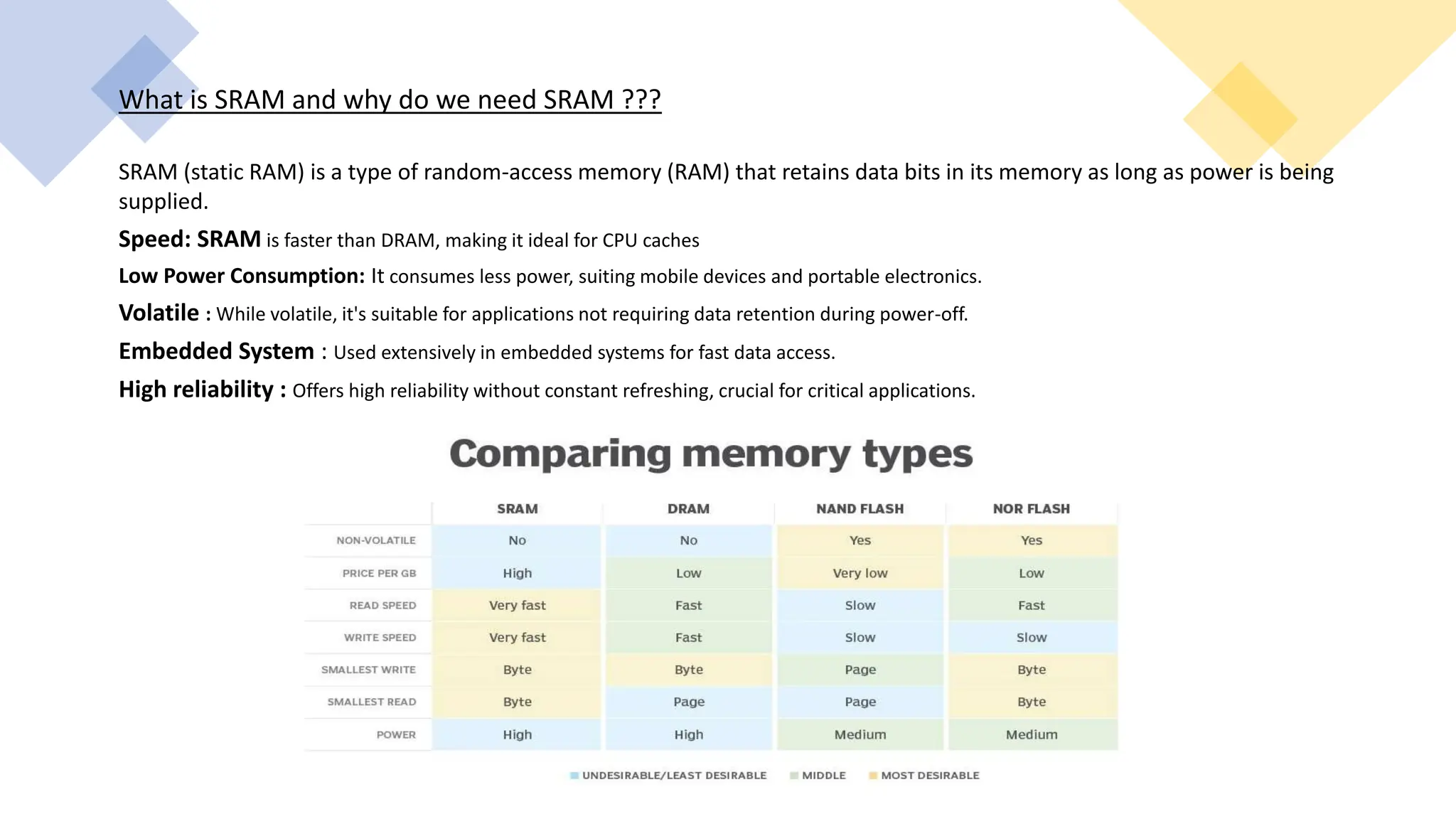
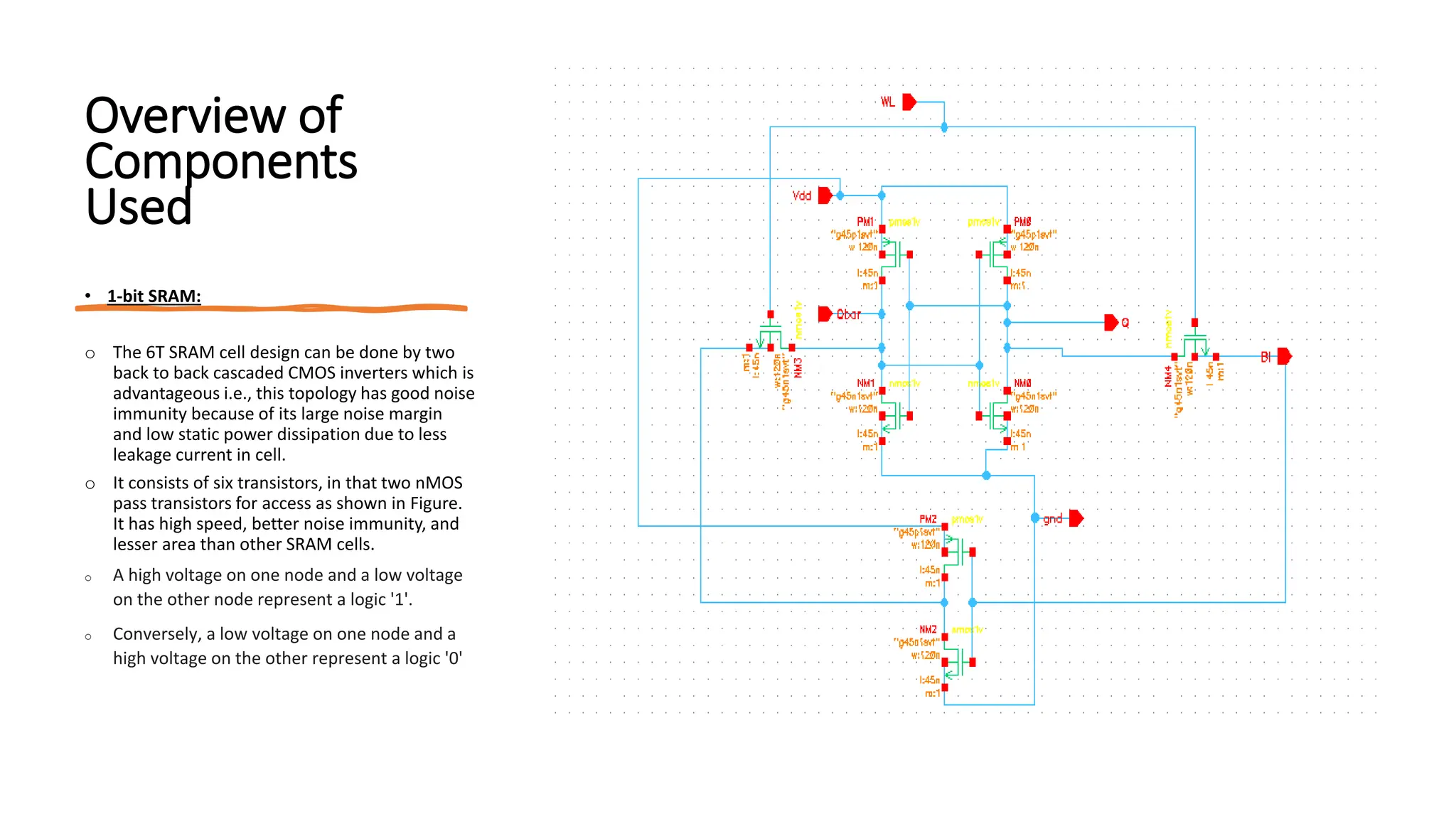
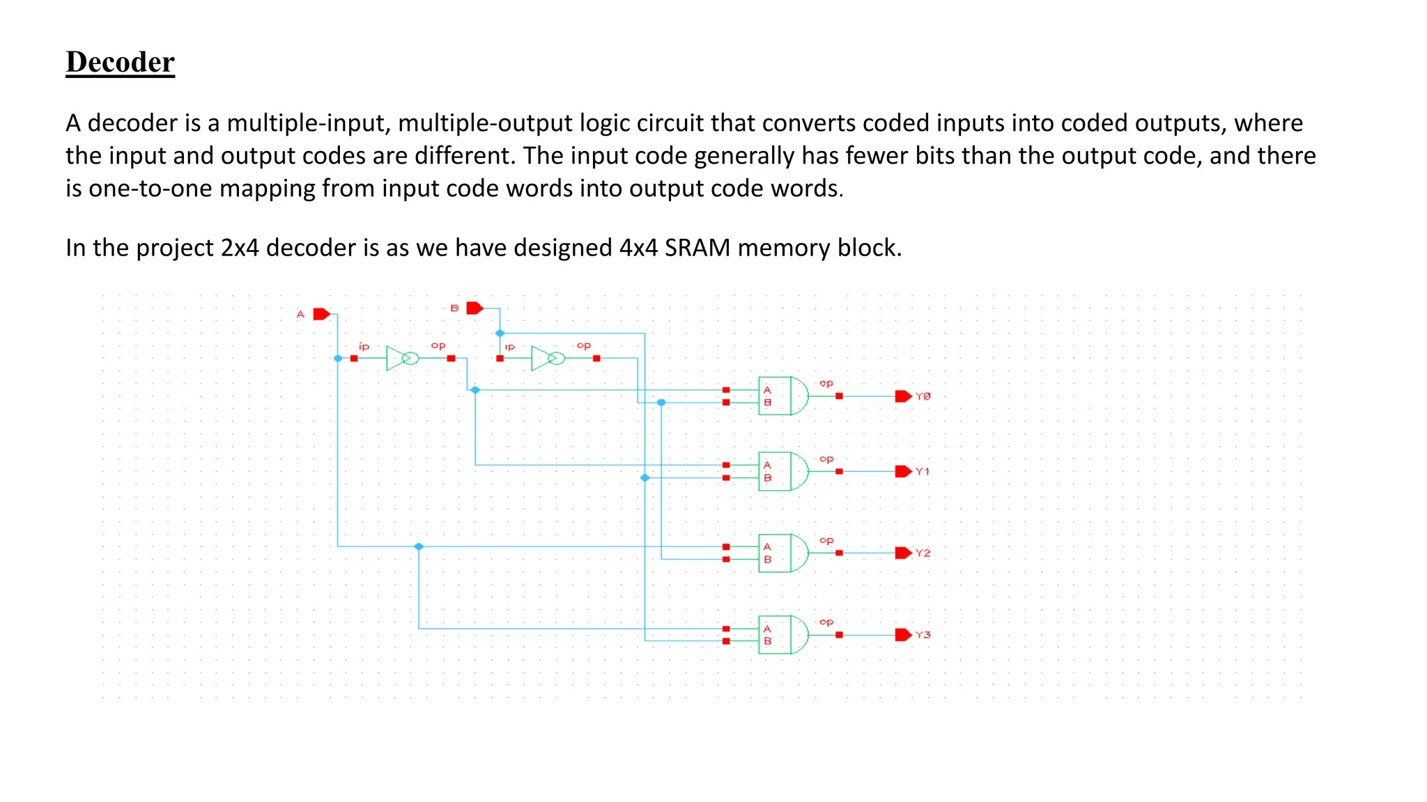
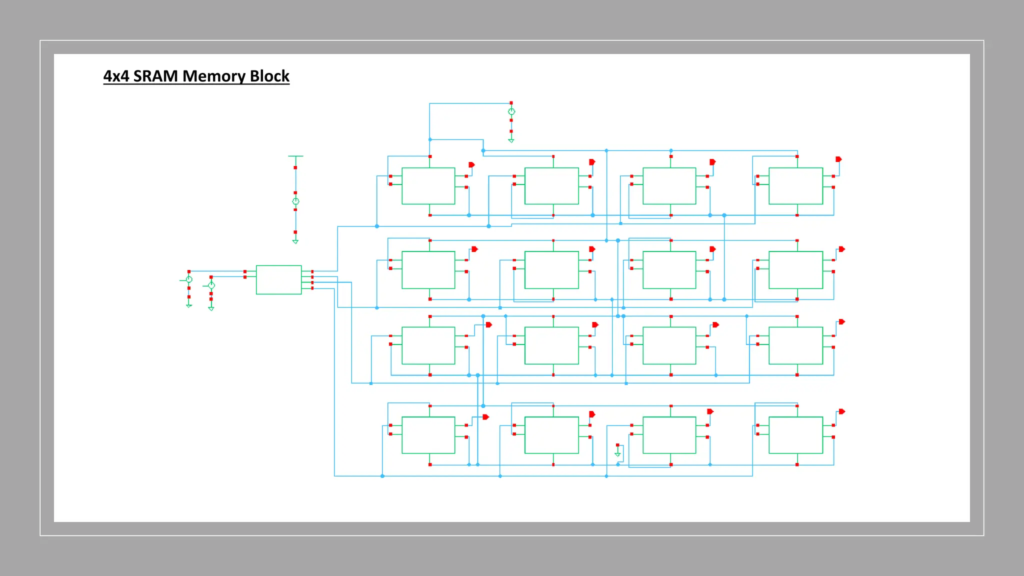
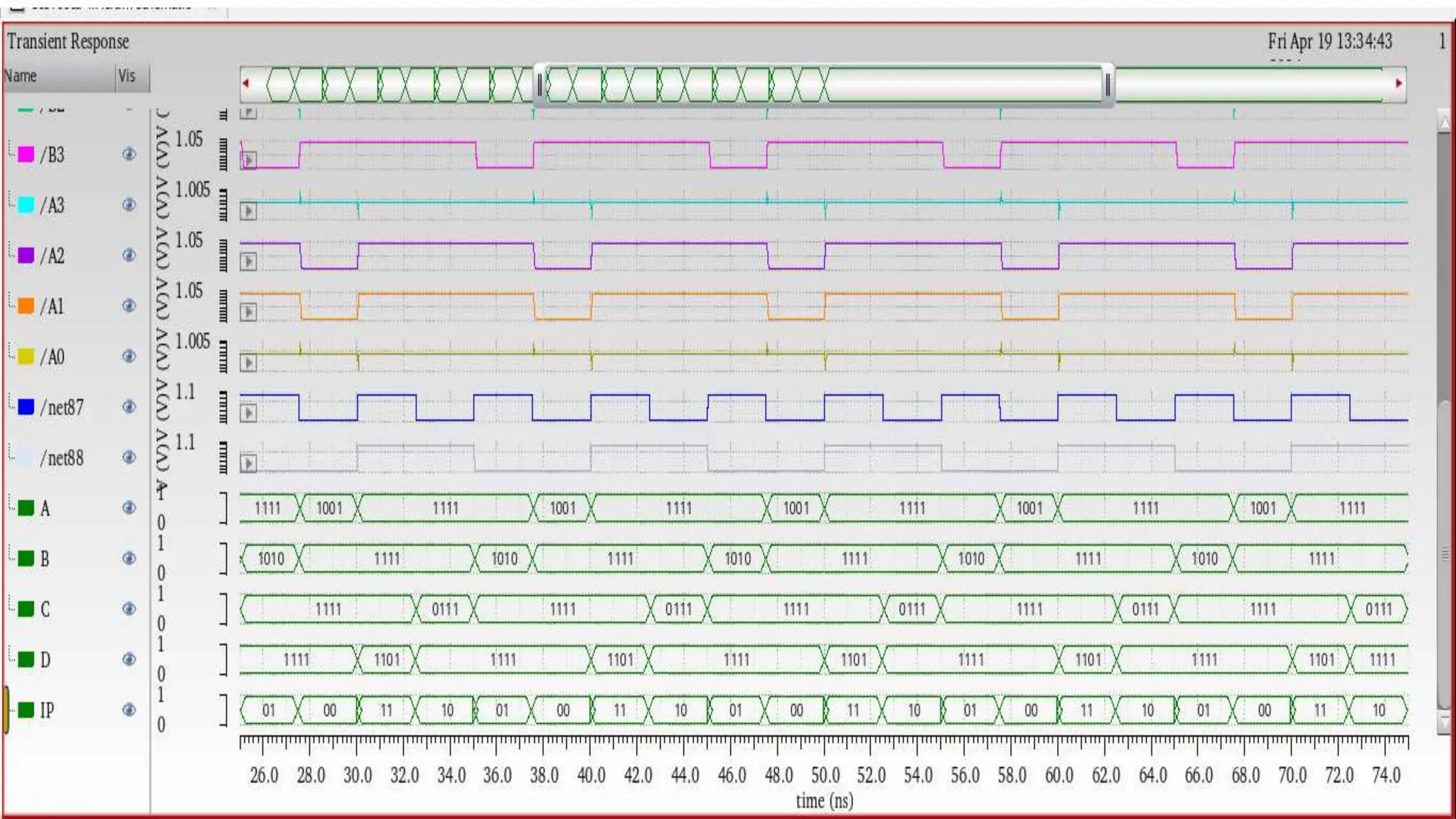
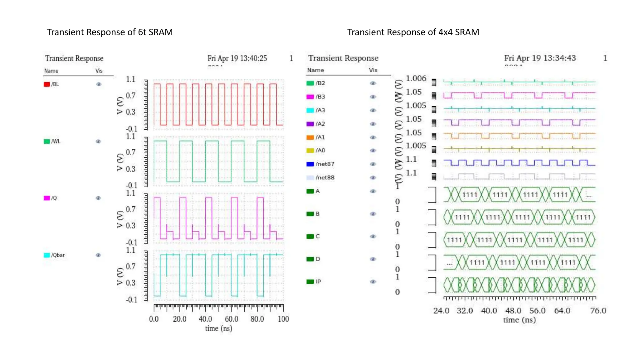
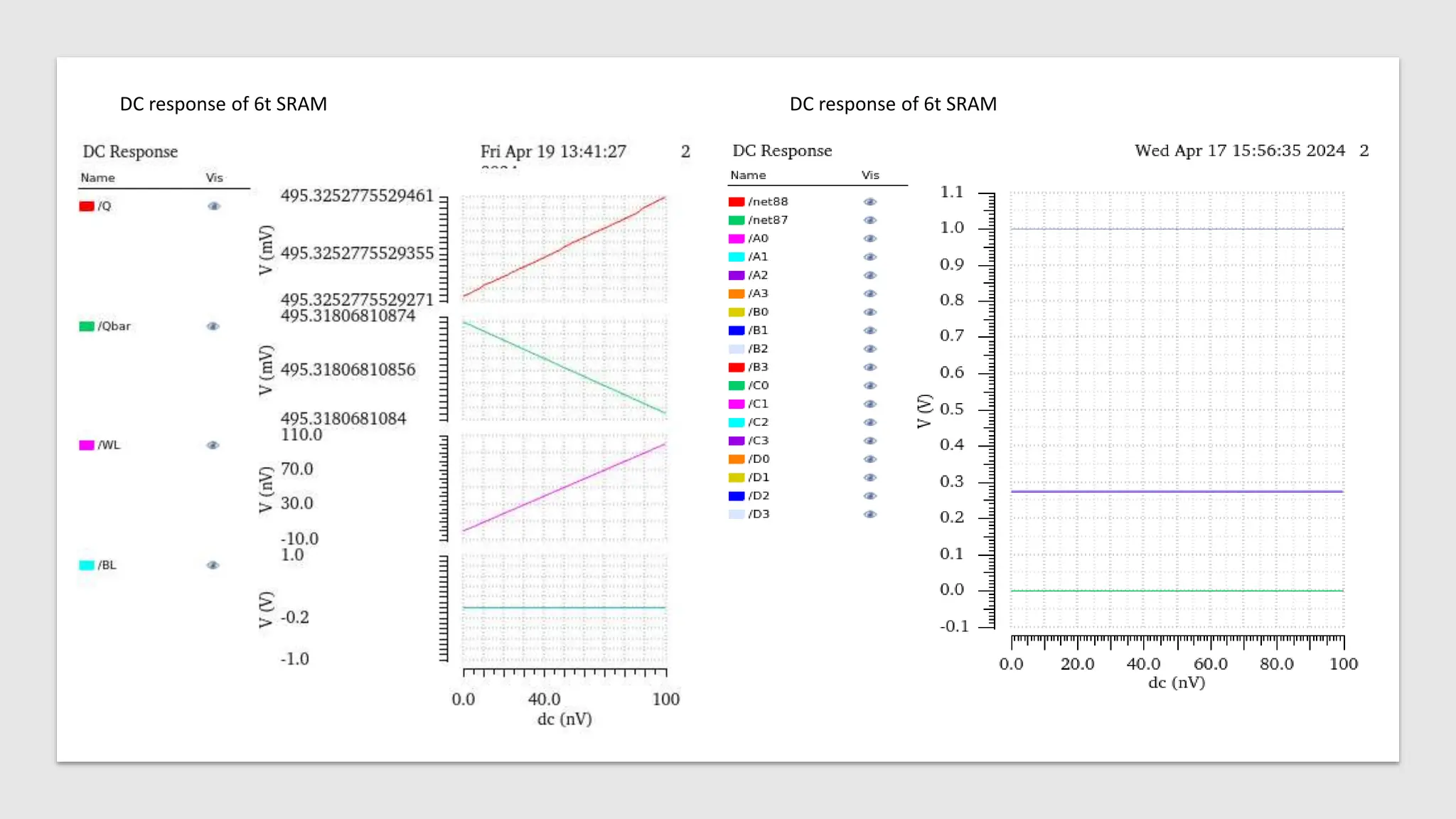
4x4 SRAM Memory Block at 45 nm node
This presentation give visuals about design and architecture of a
compact 4x4 SRAM memory block, a crucial component in modern
digital systems. Discover how this efficient memory solution enables
high-speed data storage and retrieval at the heart of various electronic
devices.
Presented by:
Jai Shivam Chaudhary
12018935
What is SRAM and why do we need SRAM ???
SRAM (static RAM) is a type of random-access memory (RAM) that retains data bits in its memory as long as power is being
supplied.
Speed: SRAM is faster than DRAM, making it ideal for CPU caches
Low Power Consumption: It consumes less power, suiting mobile devices and portable electronics.
Volatile : While volatile, it's suitable for applications not requiring data retention during power-off.
Embedded System : Used extensively in embedded systems for fast data access.
High reliability : Offers high reliability without constant refreshing, crucial for critical applications.
Overview of
Components
Used
• 1-bit SRAM:
o The 6T SRAM cell design can be done by two
back to back cascaded CMOS inverters which is
advantageous i.e., this topology has good noise
immunity because of its large noise margin
and low static power dissipation due to less
leakage current in cell.
o It consists of six transistors, in that two nMOS
pass transistors for access as shown in Figure.
It has high speed, better noise immunity, and
lesser area than other SRAM cells.
o A high voltage on one node and a low voltage
on the other node represent a logic '1'.
o Conversely, a low voltage on one node and a
high voltage on the other represent a logic '0'
Decoder
A decoder is a multiple-input, multiple-output logic circuit that converts coded inputs into coded outputs, where
the input and output codes are different. The input code generally has fewer bits than the output code, and there
is one-to-one mapping from input code words into output code words.
In the project 2x4 decoder is as we have designed 4x4 SRAM memory block.
Schematic and layout of 4x4 SRAM array
The 4x4 SRAM array consists of 16 individual 1-
bit SRAM cells arranged in a grid. Each cell has
access transistors controlled by row and column
select lines for read and write operations. The
cells are connected to a common bitline and
bitline complement, allowing data to be read and
written.
The layout of the 4x4 array leverages the
compact design of the 1-bit SRAM cell,
replicating it in a grid pattern. Careful routing of
the word lines, bitlines, and power/ground
connections ensures efficient use of the
available area.
Addressing and Decoding Logic
1 Address Decoder
The address decoder takes the row and column addresses as inputs and
activates the corresponding wordline and bitline in the SRAM array.
2 Row Decoder
The row decoder selects the appropriate row based on the row address,
enabling access to the desired SRAM cells along that row.
3 Column Decoder
The column decoder selects the appropriate column based on the column
address, connecting the selected bitlines to the data bus for read/write
operations.
Design and Implementation
This is the symbol of 1-bit SRAM that has been used to make the grid or array
of 4x4 SRAM Memory block.
To design 4x4 SRAM array we have used 4 rows, and 4 columns means total 16
1-bit 6T SRAM cell blocks and all blocks are connected and configured
together and for data input across all cell decoder has been used to take 4
different bit values in form of ‘0’ and ‘1’.
In SRAM (Static Random Access Memory), the bit line and word line are essential components for accessing and
storing data:
Bit Line: The bit line is a pathway used to transfer data in and out of the memory cell. It connects
to one side of each memory cell within the SRAM array. During read and write operations, data travels through
the bit line to access or modify the stored information in the memory cell.
Word Line: The word line, also known as the row line,selects a specific row of memory cells within the SRAM array.
When activated, the word line enables the data stored in the selected row to be accessed via the associated bit lines.
It controls the read and write operations by activating the appropriate row of memory cells
, allowing the data to flow through the bit lines.
Selection line Values provided
Y0 1001
Y1 1010
Y2 0111
Y3 1101
4x4 SRAM Memory Block
Transient Response of 6t SRAM Transient Response of 4x4 SRAM
DC response of 6t SRAM DC response of 6t SRAM
Power and Performance Considerations
Power
Consumption
Minimizing power
consumption is
crucial for the 4x4
SRAM memory
block. Careful
transistor sizing and
circuit design
techniques should
be employed to
reduce both static
and dynamic power
dissipation.
Operating Speed
The memory block
must deliver fast
access times and
high throughput to
meet performance
requirements.
Optimizing the
addressing logic,
read/write circuitry,
and memory array
layout can help
achieve the desired
speed.
Leakage
Reduction
Transistor leakage is
a significant
contributor to power
consumption in
modern CMOS
technologies.
Employing
appropriate
transistor sizing,
well biasing, and
other leakage
reduction
techniques can help
mitigate this issue.
Thermal
Management
The memory block's
heat dissipation
must be considered,
as high
temperatures can
degrade
performance and
reliability. Thermal-
aware layout and
packaging solutions
should be explored
to ensure the design
operates within safe
limits.
Conclusion and future improvements
Optimized Design
The 4x4 SRAM memory block design can
be further optimized for power,
performance, and area by exploring
advanced transistor technologies and circuit
techniques.
Scalability
The architecture can be scaled to larger
SRAM arrays to meet the growing demand
for on-chip memory in modern SoCs.
Enhanced Reliability
Incorporating error detection and correction
mechanisms can improve the overall
reliability and robustness of the SRAM
design.
Integration with Peripherals
Seamless integration of the SRAM block
with peripheral circuitry, such as address
decoders and I/O buffers, can enhance the
overall system performance.

Introduction-to-4x4-SRAM-Memory-Block.pptx

  • 1.
    4x4 SRAM MemoryBlock at 45 nm node This presentation give visuals about design and architecture of a compact 4x4 SRAM memory block, a crucial component in modern digital systems. Discover how this efficient memory solution enables high-speed data storage and retrieval at the heart of various electronic devices. Presented by: Jai Shivam Chaudhary 12018935
  • 2.
    What is SRAMand why do we need SRAM ??? SRAM (static RAM) is a type of random-access memory (RAM) that retains data bits in its memory as long as power is being supplied. Speed: SRAM is faster than DRAM, making it ideal for CPU caches Low Power Consumption: It consumes less power, suiting mobile devices and portable electronics. Volatile : While volatile, it's suitable for applications not requiring data retention during power-off. Embedded System : Used extensively in embedded systems for fast data access. High reliability : Offers high reliability without constant refreshing, crucial for critical applications.
  • 3.
    Overview of Components Used • 1-bitSRAM: o The 6T SRAM cell design can be done by two back to back cascaded CMOS inverters which is advantageous i.e., this topology has good noise immunity because of its large noise margin and low static power dissipation due to less leakage current in cell. o It consists of six transistors, in that two nMOS pass transistors for access as shown in Figure. It has high speed, better noise immunity, and lesser area than other SRAM cells. o A high voltage on one node and a low voltage on the other node represent a logic '1'. o Conversely, a low voltage on one node and a high voltage on the other represent a logic '0'
  • 4.
    Decoder A decoder isa multiple-input, multiple-output logic circuit that converts coded inputs into coded outputs, where the input and output codes are different. The input code generally has fewer bits than the output code, and there is one-to-one mapping from input code words into output code words. In the project 2x4 decoder is as we have designed 4x4 SRAM memory block.
  • 5.
    Schematic and layoutof 4x4 SRAM array The 4x4 SRAM array consists of 16 individual 1- bit SRAM cells arranged in a grid. Each cell has access transistors controlled by row and column select lines for read and write operations. The cells are connected to a common bitline and bitline complement, allowing data to be read and written. The layout of the 4x4 array leverages the compact design of the 1-bit SRAM cell, replicating it in a grid pattern. Careful routing of the word lines, bitlines, and power/ground connections ensures efficient use of the available area.
  • 6.
    Addressing and DecodingLogic 1 Address Decoder The address decoder takes the row and column addresses as inputs and activates the corresponding wordline and bitline in the SRAM array. 2 Row Decoder The row decoder selects the appropriate row based on the row address, enabling access to the desired SRAM cells along that row. 3 Column Decoder The column decoder selects the appropriate column based on the column address, connecting the selected bitlines to the data bus for read/write operations.
  • 7.
    Design and Implementation Thisis the symbol of 1-bit SRAM that has been used to make the grid or array of 4x4 SRAM Memory block. To design 4x4 SRAM array we have used 4 rows, and 4 columns means total 16 1-bit 6T SRAM cell blocks and all blocks are connected and configured together and for data input across all cell decoder has been used to take 4 different bit values in form of ‘0’ and ‘1’.
  • 8.
    In SRAM (StaticRandom Access Memory), the bit line and word line are essential components for accessing and storing data: Bit Line: The bit line is a pathway used to transfer data in and out of the memory cell. It connects to one side of each memory cell within the SRAM array. During read and write operations, data travels through the bit line to access or modify the stored information in the memory cell. Word Line: The word line, also known as the row line,selects a specific row of memory cells within the SRAM array. When activated, the word line enables the data stored in the selected row to be accessed via the associated bit lines. It controls the read and write operations by activating the appropriate row of memory cells , allowing the data to flow through the bit lines. Selection line Values provided Y0 1001 Y1 1010 Y2 0111 Y3 1101
  • 9.
  • 11.
    Transient Response of6t SRAM Transient Response of 4x4 SRAM
  • 12.
    DC response of6t SRAM DC response of 6t SRAM
  • 13.
    Power and PerformanceConsiderations Power Consumption Minimizing power consumption is crucial for the 4x4 SRAM memory block. Careful transistor sizing and circuit design techniques should be employed to reduce both static and dynamic power dissipation. Operating Speed The memory block must deliver fast access times and high throughput to meet performance requirements. Optimizing the addressing logic, read/write circuitry, and memory array layout can help achieve the desired speed. Leakage Reduction Transistor leakage is a significant contributor to power consumption in modern CMOS technologies. Employing appropriate transistor sizing, well biasing, and other leakage reduction techniques can help mitigate this issue. Thermal Management The memory block's heat dissipation must be considered, as high temperatures can degrade performance and reliability. Thermal- aware layout and packaging solutions should be explored to ensure the design operates within safe limits.
  • 14.
    Conclusion and futureimprovements Optimized Design The 4x4 SRAM memory block design can be further optimized for power, performance, and area by exploring advanced transistor technologies and circuit techniques. Scalability The architecture can be scaled to larger SRAM arrays to meet the growing demand for on-chip memory in modern SoCs. Enhanced Reliability Incorporating error detection and correction mechanisms can improve the overall reliability and robustness of the SRAM design. Integration with Peripherals Seamless integration of the SRAM block with peripheral circuitry, such as address decoders and I/O buffers, can enhance the overall system performance.