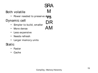
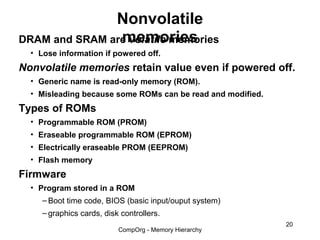
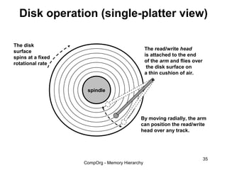
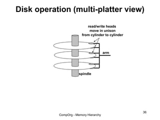
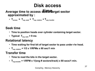
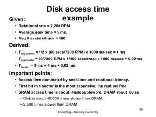
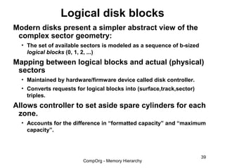
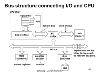
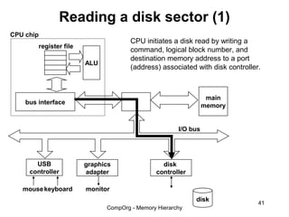
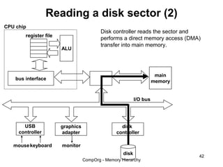
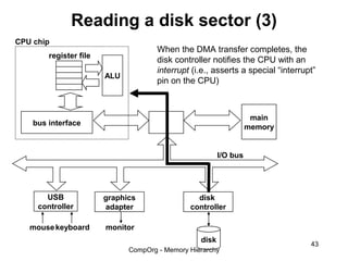
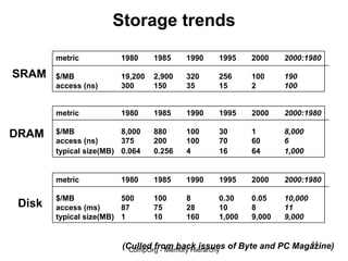
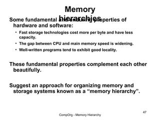
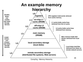
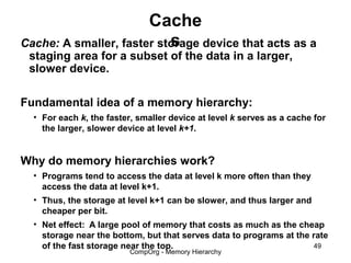
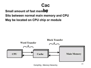
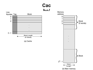
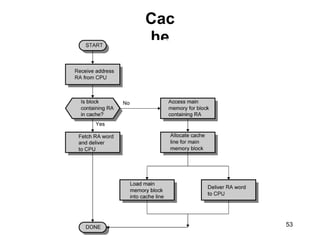
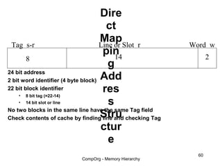
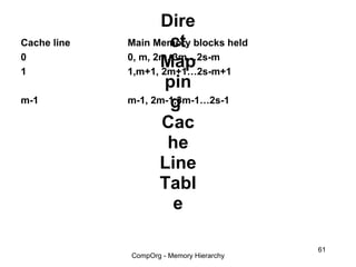
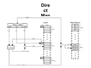
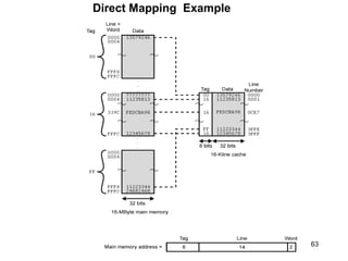
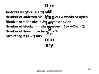
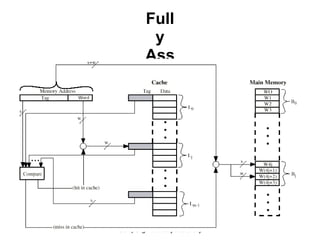
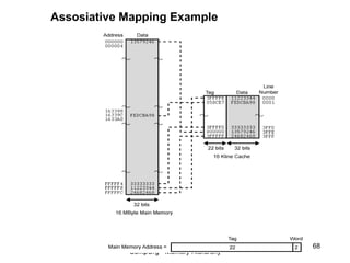
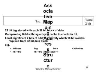
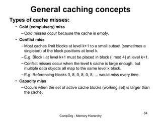
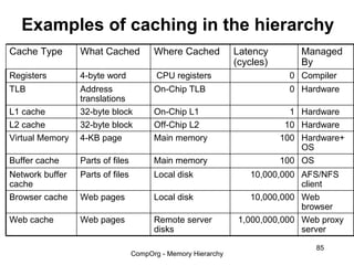
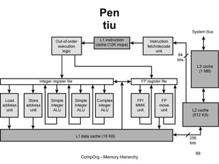
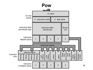
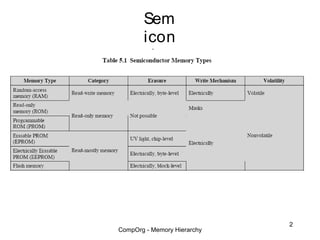
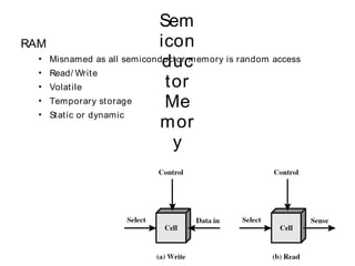
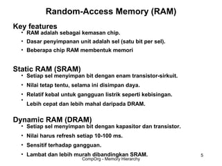
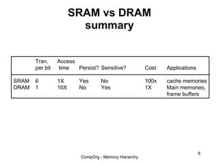
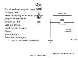
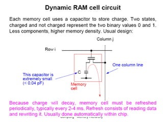
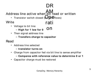
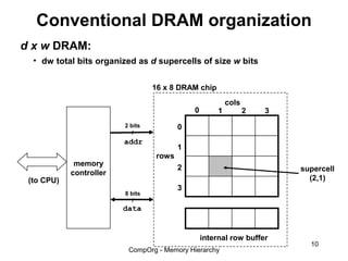
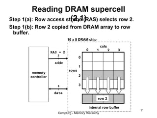
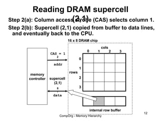
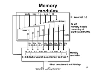
Implementation of High Reliable 6T SRAM Cell Designiosrjce
Memory can be formed with the integration of large number of basic storing element called cells.
SRAM cell is one of the basic storing unit of volatile semiconductor memory that stores binary logic '1' or '0' bit.
Modified read and write circuits were proposed in this paper to address incorrect read and write operations in
conventional 6T SRAM cell design available in open literature. Design of a new highly reliable 6T SRAM cell
design is proposed with reliable read, write operations and negative bit line voltage (NBLV). Simulations are
carried out using MENTOR GRAPHICS
Design and Simulation Low power SRAM Circuitsijsrd.com
SRAMs), focusing on optimizing delay and power. As the scaling trends in the speed and power of SRAMs with size and technology and find that the SRAM delay scales as the logarithm of its size as long as the interconnect delay is negligible. Non-scaling of threshold mismatches with process scaling, causes the signal swings in the bitlines and data lines also not to scale, leading to an increase in the relative delay of an SRAM, across technology generations. Appropriate methods for reduction of power consumption were studied such as capacitance reduction, very low operating voltages, DC and AC current reduction and suppression of leakage currents to name a few.. Many of reviewed techniques are applicable to other applications such as ASICs, DSPs, etc. Battery and solar-cell operation requires an operating voltage environment in low voltage area. These conditions demand new design approaches and more sophisticated concepts to retain high device reliability. The proposed techniques (USRS and LPRS) are topology based and hence easier to implement.
Designed a fully customized 128x10b SRAM by constructing schematic & virtuoso layout of memory cell array (6T cell), row & column decoder, pre-charge circuit, write circuit and sense amplifier using Cadence. Manually placed and routed all components, performed DRC & LVS debugging of constructed schematic and layout and ran PEX to generate the final Netlist, Hspice Spectre simulation of final design for verification of the correct functionality and analysis of best read, best write cycles & the worst case timing for read and write. Timing and power consumed is analyzed through STA-Primetime (Static timing Analysis)
In the project#1, IBM 130nm process is used to design and manual layout a 128 word SRAM, with word size 10bits. Cadence's Virtuoso is applied for layout editing, DRC and LVS running and circuit simulation.
Memory map selection of real time sdram controller using verilog full project...rahul kumar verma
full report on Memory map selection of real time SDRAM controller using verilog which was my project.If you want any help email me @ rahulverma2512@gmail.com
This is a project implemented in VHDL. It is design of a multi-level cache memory for a uni-processor system. The document also includes some of the simulation and synthesis results.
250nm Technology Based Low Power SRAM Memoryiosrjce
High integration density, low power and fastperformance are all critical parameters in designing of
memory blocks. Static Random Access Memories (SRAMs)’s focusing on optimizing dynamic power concept of
virtual source transistors is used for removing direct connection between VDD and GND.
Also stacking effect can be reduced by switching off the stacktransistors when the memory is ideal and the
leakage current using SVL techniques This paper discusses the evolution of 9t SRAM circuits in terms of low
power consumption, The whole circuit verification is done on the Tanner tool, Schematic of the
SRAM cell is designed on the S-Edit and net list simulation done by using T-spice and waveforms are analyzed
through the W-edit
Time and Low Power Operation Using Embedded Dram to Gain Cell Data RetentionIJMTST Journal
Logic compatible gain cell (GC)-embedded DRAM (eDRAM) arrays are considered an alternative to SRAM because of their small size, non rationed operation, low static leakage, and two port functionality. But traditional GC-eDRAM implementations require boosted control signals in order to write full voltage levels to the cell to reduce the refresh rate and shorten access times. The boosted levels require an extra power supply or on-chip charge pumps, as well as nontrivial level shifting and toleration of high voltage levels. In this paper, we present a novel, logic compatible, 3T GC-eDRAM bit cell that operates with a single-supply voltage and provides superior write capability to the conventional GC structures. The proposed circuit is demonstrated in 0.25μm CMOS process targeted at low power, energy efficient application.
Talk on Fundamentals of Parallel Computing ranging from basics and history of parallel computing to comparison of recent trends in the area of high performance computing delivered at Indo-German Winter Academy 2009.
Biological screening of herbal drugs: Introduction and Need for
Phyto-Pharmacological Screening, New Strategies for evaluating
Natural Products, In vitro evaluation techniques for Antioxidants, Antimicrobial and Anticancer drugs. In vivo evaluation techniques
for Anti-inflammatory, Antiulcer, Anticancer, Wound healing, Antidiabetic, Hepatoprotective, Cardio protective, Diuretics and
Antifertility, Toxicity studies as per OECD guidelines
How to Make a Field invisible in Odoo 17Celine George
It is possible to hide or invisible some fields in odoo. Commonly using “invisible” attribute in the field definition to invisible the fields. This slide will show how to make a field invisible in odoo 17.
Introduction to AI for Nonprofits with Tapp NetworkTechSoup
Dive into the world of AI! Experts Jon Hill and Tareq Monaur will guide you through AI's role in enhancing nonprofit websites and basic marketing strategies, making it easy to understand and apply.
Embracing GenAI - A Strategic ImperativePeter Windle
Artificial Intelligence (AI) technologies such as Generative AI, Image Generators and Large Language Models have had a dramatic impact on teaching, learning and assessment over the past 18 months. The most immediate threat AI posed was to Academic Integrity with Higher Education Institutes (HEIs) focusing their efforts on combating the use of GenAI in assessment. Guidelines were developed for staff and students, policies put in place too. Innovative educators have forged paths in the use of Generative AI for teaching, learning and assessments leading to pockets of transformation springing up across HEIs, often with little or no top-down guidance, support or direction.
This Gasta posits a strategic approach to integrating AI into HEIs to prepare staff, students and the curriculum for an evolving world and workplace. We will highlight the advantages of working with these technologies beyond the realm of teaching, learning and assessment by considering prompt engineering skills, industry impact, curriculum changes, and the need for staff upskilling. In contrast, not engaging strategically with Generative AI poses risks, including falling behind peers, missed opportunities and failing to ensure our graduates remain employable. The rapid evolution of AI technologies necessitates a proactive and strategic approach if we are to remain relevant.
2024.06.01 Introducing a competency framework for languag learning materials ...Sandy Millin
http://sandymillin.wordpress.com/iateflwebinar2024
Published classroom materials form the basis of syllabuses, drive teacher professional development, and have a potentially huge influence on learners, teachers and education systems. All teachers also create their own materials, whether a few sentences on a blackboard, a highly-structured fully-realised online course, or anything in between. Despite this, the knowledge and skills needed to create effective language learning materials are rarely part of teacher training, and are mostly learnt by trial and error.
Knowledge and skills frameworks, generally called competency frameworks, for ELT teachers, trainers and managers have existed for a few years now. However, until I created one for my MA dissertation, there wasn’t one drawing together what we need to know and do to be able to effectively produce language learning materials.
This webinar will introduce you to my framework, highlighting the key competencies I identified from my research. It will also show how anybody involved in language teaching (any language, not just English!), teacher training, managing schools or developing language learning materials can benefit from using the framework.
The French Revolution, which began in 1789, was a period of radical social and political upheaval in France. It marked the decline of absolute monarchies, the rise of secular and democratic republics, and the eventual rise of Napoleon Bonaparte. This revolutionary period is crucial in understanding the transition from feudalism to modernity in Europe.
For more information, visit-www.vavaclasses.com
Synthetic Fiber Construction in lab .pptxPavel ( NSTU)
Synthetic fiber production is a fascinating and complex field that blends chemistry, engineering, and environmental science. By understanding these aspects, students can gain a comprehensive view of synthetic fiber production, its impact on society and the environment, and the potential for future innovations. Synthetic fibers play a crucial role in modern society, impacting various aspects of daily life, industry, and the environment. ynthetic fibers are integral to modern life, offering a range of benefits from cost-effectiveness and versatility to innovative applications and performance characteristics. While they pose environmental challenges, ongoing research and development aim to create more sustainable and eco-friendly alternatives. Understanding the importance of synthetic fibers helps in appreciating their role in the economy, industry, and daily life, while also emphasizing the need for sustainable practices and innovation.
Operation “Blue Star” is the only event in the history of Independent India where the state went into war with its own people. Even after about 40 years it is not clear if it was culmination of states anger over people of the region, a political game of power or start of dictatorial chapter in the democratic setup.
The people of Punjab felt alienated from main stream due to denial of their just demands during a long democratic struggle since independence. As it happen all over the word, it led to militant struggle with great loss of lives of military, police and civilian personnel. Killing of Indira Gandhi and massacre of innocent Sikhs in Delhi and other India cities was also associated with this movement.
Normal Labour/ Stages of Labour/ Mechanism of LabourWasim Ak
Normal labor is also termed spontaneous labor, defined as the natural physiological process through which the fetus, placenta, and membranes are expelled from the uterus through the birth canal at term (37 to 42 weeks
Acetabularia Information For Class 9 .docxvaibhavrinwa19
Acetabularia acetabulum is a single-celled green alga that in its vegetative state is morphologically differentiated into a basal rhizoid and an axially elongated stalk, which bears whorls of branching hairs. The single diploid nucleus resides in the rhizoid.
2. Sem
icon
duc
tor
Me
m or
y
Typ
es
2
CompOrg - Memory Hierarchy
3. Sem
RAM icon
duc
• Misnamed as all semiconduct or memory is random access
• Read/ Writ e
• Volat ile tor
• Temporary st orage Me
• St at ic or dynamic
m or
y
3
CompOrg - Memory Hierarchy
5. Random-Access Memory (RAM)
Key features
• RAM adalah sebagai kemasan chip.
• Dasar penyimpanan unit adalah sel (satu bit per sel).
• Beberapa chip RAM membentuk memori
Static RAM (SRAM)
• Setiap sel menyimpan bit dengan enam transistor-sirkuit.
• Nilai tetap tentu, selama ini disimpan daya.
• Relatif kebal untuk gangguan listrik seperti kebisingan.
•
Lebih cepat dan lebih mahal daripada DRAM.
Dynamic RAM (DRAM)
• Setiap sel menyimpan bit dengan kapasitor dan transistor.
• Nilai harus refresh setiap 10-100 ms.
• Sensitif terhadap gangguan.
• Lambat dan lebih murah dibandingkan SRAM. 5
CompOrg - Memory Hierarchy
6. SRAM vs DRAM
summary
Tran. Access
per bit time Persist? Sensitive? Cost Applications
SRAM 6 1X Yes No 100x cache memories
DRAM 1 10X No Yes 1X Main memories,
frame buffers
6
CompOrg - Memory Hierarchy
7. Dyn
Bit s st ored as charge in capacit ors i
am
Charges leak
Need refreshing even when powered
c
Simpler const ruct ion RA
Smaller per bit M
Less ex pensive
Need refresh circuit s
Slower
Main memory
Essent ially analogue
• Level of charge det ermines value
7
CompOrg - Memory Hierarchy
9. DR
Address line active when bit read
AM or writt en
Ope
• Transist or swit ch closed (current flows)
Write rati
• Volt age t o bit line
– High for 1 low for 0 on
• Then signal address line
– Transfers charge to capacitor
Read
• Address line select ed
– transistor turns on
• Charge from capacit or fed via bit line t o sense amplifier
– Compares with reference value to determine 0 or 1
• Capacit or charge must be rest ored
9
CompOrg - Memory Hierarchy
10. Conventional DRAM organization
d x w DRAM:
• dw total bits organized as d supercells of size w bits
16 x 8 DRAM chip
cols
0 1 2 3
2 bits 0
/
addr
1
rows
memory
2 supercell
controller
(to CPU) (2,1)
3
8 bits
/
data
internal row buffer
10
CompOrg - Memory Hierarchy
11. Reading DRAM supercell
(2,1)
Step 1(a): Row access strobe (RAS) selects row 2.
Step 1(b): Row 2 copied from DRAM array to row
buffer.
16 x 8 DRAM chip
cols
0 1 2 3
RAS = 2
2
/ 0
addr
1
rows
memory
controller 2
8 3
/
data
row 2
internal row buffer
11
CompOrg - Memory Hierarchy
12. Reading DRAM supercell
(2,1)
Step 2(a): Column access strobe (CAS) selects column 1.
Step 2(b): Supercell (2,1) copied from buffer to data lines,
and eventually back to the CPU.
16 x 8 DRAM chip
cols
0 1 2 3
CAS = 1
2
/ 0
addr
1
rows
memory
controller supercell 2
(2,1)
8 3
/
data
internal row buffer
12
CompOrg - Memory Hierarchy
13. Memory
modules
addr (row = i, col = j)
: supercell (i,j)
DRAM 0
64 MB
memory module
consisting of
DRAM 7
eight 8Mx8 DRAMs
data
bits bits bits bits bits bits bits bits
56-63 48-55 40-47 32-39 24-31 16-23 8-15 0-7
63 56 55 48 47 40 39 32 31 24 23 16 15 8 7 0
Memory
controller
64-bit doubleword at main memory address A
64-bit doubleword to CPU chip
13
CompOrg - Memory Hierarchy
14. Enhanced
DRAMs
All enhanced DRAMs are built around the conventional
DRAM core.
• Fast page mode DRAM (FPM DRAM)
– Access contents of row with [RAS, CAS, CAS, CAS, CAS] instead of
[(RAS,CAS), (RAS,CAS), (RAS,CAS), (RAS,CAS)].
• Extended data out DRAM (EDO DRAM)
– Enhanced FPM DRAM with more closely spaced CAS signals.
• Synchronous DRAM (SDRAM)
– Driven with rising clock edge instead of asynchronous control signals.
• Double data-rate synchronous DRAM (DDR SDRAM)
– Enhancement of SDRAM that uses both clock edges as control signals.
• Video RAM (VRAM)
– Like FPM DRAM, but output is produced by shifting row buffer
– Dual ported (allows concurrent reads and writes)
14
CompOrg - Memory Hierarchy
15. Stat
ic
Bit s stored as on/ off swit ches
No charges t o leak RA
No refreshing needed when powered
M
More complex construction
Larger per bit
More ex pensive
Does not need refresh circuits
Fast er
Cache
Digital
• Uses flip-flops
15
CompOrg - Memory Hierarchy
17. Stat
ing
RA
M
Stru
ctur
e
17
CompOrg - Memory Hierarchy
18. Stat
ic stable logic state
Transistor arrangement gives
St ate 1 RA
• C high, C low
1 2 M
• T T off, T T on
1 4 2 3
Ope
St ate 0
• C high, C low
2 1
rati
• T T off, T T on
2 3 1 4
on
Address line transistors T5 T6 is switch
Write – apply value to B & compliment t o B
Read – value is on line B
18
CompOrg - Memory Hierarchy
19. SRA
Both volatile M
vs
• Power needed t o preserve dat a
Dynamic cell
• Simpler t o build, smaller
DR
• More dense AM
• Less ex pensive
• Needs refresh
• Larger memory unit s
St atic
• Fast er
• Cache
19
CompOrg - Memory Hierarchy
20. Nonvolatile
memories
DRAM and SRAM are volatile memories
• Lose information if powered off.
Nonvolatile memories retain value even if powered off.
• Generic name is read-only memory (ROM).
• Misleading because some ROMs can be read and modified.
Types of ROMs
• Programmable ROM (PROM)
• Eraseable programmable ROM (EPROM)
• Electrically eraseable PROM (EEPROM)
• Flash memory
Firmware
• Program stored in a ROM
– Boot time code, BIOS (basic input/ouput system)
– graphics cards, disk controllers.
20
CompOrg - Memory Hierarchy
21. Rea
Permanent storage d
• Nonvolat ile
Onl
Microprogramming (see later)
Library subroutines
y
Systems programs (BIOS) Me
Function tables m or
y
(RO
M)
21
CompOrg - Memory Hierarchy
22. Typ
Written during manufacture es
of
• Very ex pensive for small runs
Programmable (once)
• PROM
RO
• Needs special equipment t o Mprogram
Read “mostly”
• Erasable Programmable (EPROM)
– Erased by UV
• Elect rically Erasable (EEPROM)
– Takes much longer to write than read
• Flash memory
– Erase whole memory electrically
22
CompOrg - Memory Hierarchy
23. Org
anis
A 16Mbit chip can be organised as 1M of 16 bit words
atio
A bit per chip system has 16 lot s of 1Mbit chip wit h
bit 1 of each word in chip 1 and so on
n in as a 2048 x 2048 x
A 16Mbit chip can be organised
4bit array det
ail column address
• Reduces number of address pins
– Multiplex row address and
– 11 pins to address (2 11 =2048)
– Adding one more pin doubles range of values so x4
capacity (2 12 x4 Capacity with 2 11 )
23
CompOrg - Memory Hierarchy
24. Bus structure connecting
CPU and memory
A bus is a collection of parallel wires that carry
address, data, and control signals.
Buses are typically shared by multiple devices.
CPU chip
register file
ALU
system bus memory bus
I/O main
bus interface
bridge memory
24
CompOrg - Memory Hierarchy
25. Memory read transaction
(1)
CPU places address A on the memory bus.
register file Load operation: movl A, %eax
ALU
%eax
main memory
I/O bridge 0
A
bus interface x A
25
CompOrg - Memory Hierarchy
26. Memory read transaction
(2)
Main memory reads A from the memory bus, retreives
word x, and places it on the bus.
register file
Load operation: movl A, %eax
ALU
%eax
main memory
I/O bridge x 0
bus interface x A
26
CompOrg - Memory Hierarchy
27. Memory read transaction
CPU read word x from the(3) and copies it into
bus
register %eax.
register file Load operation: movl A, %eax
ALU
%eax x
main memory
I/O bridge 0
bus interface x A
27
CompOrg - Memory Hierarchy
28. Memory write transaction
(1)
CPU places address A on bus. Main memory reads it
and waits for the corresponding data word to arrive.
register file Store operation: movl %eax, A
ALU
%eax y
main memory
I/O bridge 0
A
bus interface A
28
CompOrg - Memory Hierarchy
29. Memory write transaction
(2)
CPU places data word y on the bus.
register file Store operation: movl %eax, A
ALU
%eax y
main memory
I/O bridge 0
y
bus interface A
29
CompOrg - Memory Hierarchy
30. Memory write transaction
(3)
Main memory read data word y from the bus and
stores it at address A.
register file
Store operation: movl %eax, A
ALU
%eax y
main memory
I/O bridge 0
bus interface y A
30
CompOrg - Memory Hierarchy
31. Disk
geometry
Disks consist of platters, each with two surfaces.
Each surface consists of concentric rings called tracks.
Each track consists of sectors separated by gaps.
tracks
surface
track k gaps
spindle
sectors
31
CompOrg - Memory Hierarchy
32. Disk geometry (muliple-platter view)
Aligned tracks form a cylinder.
cylinder k
surface 0
platter 0
surface 1
surface 2
platter 1
surface 3
surface 4
platter 2
surface 5
spindle
32
CompOrg - Memory Hierarchy
33. Disk
capacity
Capacity: maximum number of bits that can be stored.
• Vendors express capacity in units of gigabytes (GB), where 1 GB =
10^6.
Capacity is determined by these technology factors:
• Recording density (bits/in): number of bits that can be squeezed into
a 1 inch segment of a track.
• Track density (tracks/in): number of tracks that can be squeezed into
a 1 inch radial segment.
• Areal density (bits/in2): product of recording and track density.
Modern disks partition tracks into disjoint subsets
called recording zones
• Each track in a zone has the same number of sectors, determined by
the circumference of innermost track.
• Each zone has a different number of sectors/track
33
CompOrg - Memory Hierarchy
34. Computing disk capacity
Capacity = (# bytes/sector) x (avg. # sectors/track) x
(# tracks/surface) x (# surfaces/platter) x
(# platters/disk)
Example:
• 512 bytes/sector
• 300 sectors/track (on average)
• 20,000 tracks/surface
• 2 surfaces/platter
• 5 platters/disk
Capacity = 512 x 300 x 20000 x 2 x 5
= 30,720,000,000
= 30.72 GB
34
CompOrg - Memory Hierarchy
35. Disk operation (single-platter view)
The disk
The read/write head
surface
is attached to the end
spins at a fixed
of the arm and flies over
rotational rate
the disk surface on
a thin cushion of air.
spindle
By moving radially, the arm
can position the read/write
head over any track.
35
CompOrg - Memory Hierarchy
36. Disk operation (multi-platter view)
read/write heads
move in unison
from cylinder to cylinder
arm
spindle
36
CompOrg - Memory Hierarchy
37. Disk access
time
Average time to access some target sector
approximated by :
• Taccess = Tavg seek + Tavg rotation + Tavg transfer
Seek time
• Time to position heads over cylinder containing target sector.
• Typical Tavg seek = 9 ms
Rotational latency
• Time waiting for first bit of target sector to pass under r/w head.
• Tavg rotation = 1/2 x 1/RPMs x 60 sec/1 min
Transfer time
• Time to read the bits in the target sector.
• Tavg transfer = 1/RPM x 1/(avg # sectors/track) x 60 secs/1 min.
37
CompOrg - Memory Hierarchy
38. Disk access time
Given: example
• Rotational rate = 7,200 RPM
• Average seek time = 9 ms.
• Avg # sectors/track = 400.
Derived:
• Tavg rotation = 1/2 x (60 secs/7200 RPM) x 1000 ms/sec = 4 ms.
• Tavg transfer = 60/7200 RPM x 1/400 secs/track x 1000 ms/sec = 0.02 ms
• Taccess = 9 ms + 4 ms + 0.02 ms
Important points:
• Access time dominated by seek time and rotational latency.
• First bit in a sector is the most expensive, the rest are free.
• SRAM access time is about 4ns/doubleword, DRAM about 60 ns
– Disk is about 40,000 times slower than SRAM,
– 2,500 times slower then DRAM.
38
CompOrg - Memory Hierarchy
39. Logical disk blocks
Modern disks present a simpler abstract view of the
complex sector geometry:
• The set of available sectors is modeled as a sequence of b-sized
logical blocks (0, 1, 2, ...)
Mapping between logical blocks and actual (physical)
sectors
• Maintained by hardware/firmware device called disk controller.
• Converts requests for logical blocks into (surface,track,sector)
triples.
Allows controller to set aside spare cylinders for each
zone.
• Accounts for the difference in “formatted capacity” and “maximum
capacity”.
39
CompOrg - Memory Hierarchy
40. Bus structure connecting I/O and CPU
CPU chip
register file
ALU
system bus memory bus
I/O main
bus interface
bridge memory
I/O bus Expansion slots for
other devices such
USB graphics disk as network adapters.
controller adapter controller
mouse keyboard monitor
disk
40
CompOrg - Memory Hierarchy
41. Reading a disk sector (1)
CPU chip
CPU initiates a disk read by writing a
register file
command, logical block number, and
destination memory address to a port
ALU
(address) associated with disk controller.
main
bus interface
memory
I/O bus
USB graphics disk
controller adapter controller
mouse keyboard monitor
disk
41
CompOrg - Memory Hierarchy
42. Reading a disk sector (2)
CPU chip
Disk controller reads the sector and
register file
performs a direct memory access (DMA)
transfer into main memory.
ALU
main
bus interface
memory
I/O bus
USB graphics disk
controller adapter controller
mouse keyboard monitor
disk
42
CompOrg - Memory Hierarchy
43. Reading a disk sector (3)
CPU chip
When the DMA transfer completes, the
register file
disk controller notifies the CPU with an
interrupt (i.e., asserts a special “interrupt”
ALU
pin on the CPU)
main
bus interface
memory
I/O bus
USB graphics disk
controller adapter controller
mouse keyboard monitor
disk
43
CompOrg - Memory Hierarchy
46. The CPU-Memory
Gap
The increasing gap between DRAM, disk, and CPU
speeds.
100,000,000
10,000,000
1,000,000
Disk seek time
100,000
DRAM access time
10,000
ns
SRAM access time
1,000
CPU cycle time
100
10
1
1980 1985 1990 1995 2000
year
46
CompOrg - Memory Hierarchy
47. Memory
hierarchies
Some fundamental and enduring properties of
hardware and software:
• Fast storage technologies cost more per byte and have less
capacity.
• The gap between CPU and main memory speed is widening.
• Well-written programs tend to exhibit good locality.
These fundamental properties complement each other
beautifully.
Suggest an approach for organizing memory and
storage systems known as a “memory hierarchy”.
47
CompOrg - Memory Hierarchy
48. An example memory
hierarchy
L0:
Smaller,
faster, registers CPU registers hold words retrieved
and from cache memory.
costlier L1: on-chip L1
(per byte) cache (SRAM)
storage L1 cache holds cache lines
devices retrieved from the L2 cache.
L2: off-chip L2
cache (SRAM) L2 cache holds cache lines
retrieved from memory.
L3: main memory
(DRAM)
Larger, Main memory holds disk
slower, blocks retrieved from local
and disks.
cheaper local secondary storage
(per byte) L4:
storage (local disks)
devices Local disks hold files
retrieved from disks on
remote network servers.
L5: remote secondary storage
(distributed file systems, Web servers)
48
CompOrg - Memory Hierarchy
49. Cache
s
Cache: A smaller, faster storage device that acts as a
staging area for a subset of the data in a larger,
slower device.
Fundamental idea of a memory hierarchy:
• For each k, the faster, smaller device at level k serves as a cache for
the larger, slower device at level k+1.
Why do memory hierarchies work?
• Programs tend to access the data at level k more often than they
access the data at level k+1.
• Thus, the storage at level k+1 can be slower, and thus larger and
cheaper per bit.
• Net effect: A large pool of memory that costs as much as the cheap
storage near the bottom, but that serves data to programs at the rate
of the fast storage near the top. 49
CompOrg - Memory Hierarchy
50. Cac
he
Small amount of fast memory
Sits between normal main memory and CPU
May be located on CPU chip or module
50
CompOrg - Memory Hierarchy
51. Cac
he/
Mai
n
Me
mor
y
Stru
ctur
e
51
CompOrg - Memory Hierarchy
52. Cac
CPU requests contents of he memory location
Check cache for this dataope
If present, get from cacherati
(fast)
If not present, read required block from main memory
to cache on –
ove
Then deliver from cache to CPU
rvie
Cache includes tags to identify which block of main
memory is in each cache slot
w
52
CompOrg - Memory Hierarchy
53. Cac
he
Rea
d
Ope
rati
on -
Flo
wch
art
53
CompOrg - Memory Hierarchy
54. Cac
Size he
Mapping Function Des
Replacement Algorithm ign
Write Policy
Block Size
Number of Caches
54
CompOrg - Memory Hierarchy
55. Size
Cost doe
• More cache is expensive
s
Speed
mat
• More cache is faster (up to a point)
ter
• Checking cache for data takes time
55
CompOrg - Memory Hierarchy
56. Typi
cal
Cac
he
Org
aniz
atio
n
56
CompOrg - Memory Hierarchy
57. Co
Processor Type
Year ofmpa L1 cachea L2 cache L3 cache
Introduction
IBM 360/85
PDP-11/70
Mainframe
Minicomputer
1968
1975
riso 16 to 32 KB
1 KB
—
—
—
—
VAX 11/780
IBM 3033
Minicomputer
Mainframe
1978
1978
n of 16 KB
64 KB
—
—
—
—
IBM 3090
Intel 80486
Mainframe
PC
1985
1989
Cac 128 to 256 KB
8 KB
—
—
—
—
Pentium
PowerPC 601
PC
PC
1993
1993
he 8 KB/8 KB
32 KB
256 to 512 KB
—
—
—
PowerPC 620
PowerPC G4
PC
PC/server
1996
1999
Size 32 KB/32 KB
32 KB/32 KB
—
256 KB to 1 MB
—
2 MB
IBM S/390 G4
IBM S/390 G6
Mainframe
Mainframe
1997
1999
s 32 KB
256 KB
256 KB
8 MB
2 MB
—
Pentium 4 PC/server 2000 8 KB/8 KB 256 KB —
High-end server/
IBM SP 2000 64 KB/32 KB 8 MB —
supercomputer
CRAY MTAb Supercomputer 2000 8 KB 2 MB —
Itanium PC/server 2001 16 KB/16 KB 96 KB 4 MB
SGI Origin 2001 High-end server 2001 32 KB/32 KB 4 MB —
Itanium 2 PC/server 2002 32 KB 256 KB 6 MB
IBM POWER5 High-end server 2003 64 KB 1.9 MB 36 MB
57
CRAY XD-1 Supercomputer CompOrg - Memory Hierarchy
2004 64 KB/64 KB 1MB —
58. Map
Cache of 64kByte pin
Cache block of 4 bytes g
• i.e. cache is 16k (2 ) lines of 4 bytes
14
16MBytes main memory
Fun
24 bit address ctio
• (2 =16M)
24 n
58
CompOrg - Memory Hierarchy
59. Dire
ct
Each block of main memory maps to only one cache
line
Map in one specific place
• i.e. if a block is in cache, it must be
Address is in two parts pin
g
Least Significant w bits identify unique word
Most Significant s bits specify one memory block
The MSBs are split into a cache line field r and a tag of
s-r (most significant)
59
CompOrg - Memory Hierarchy
60. Dire
ct
Tag s-r
MapSlot r
Line or Word w
pin 14 2
8
g
24 bit address
2 bit word identifier (4 byte block) Add
22 bit block identifier
• 8 bit tag (=22-14)
res
• 14 bit slot or line s
No two blocks in the same line have the same Tag field
Stru
Check contents of cache by finding line and checking Tag
ctur
e
60
CompOrg - Memory Hierarchy
61. Dire
Cache line ct
Main Memory blocks held
0 0, m, 2m, 3m…2s-m
1
Map
1,m+1, 2m+1…2s-m+1
pin
m-1 g
m-1, 2m-1,3m-1…2s-1
Cac
he
Line
Tabl
e
61
CompOrg - Memory Hierarchy
62. Dire
ct
Map
pin
g
Cac
he
Org
aniz
atio
n
62
CompOrg - Memory Hierarchy
64. Dire
ct
Address length = (s + w) bits
Map
Number of addressable units = 2s+w words or bytes
Block size = line size = 2w words or bytes
pin
Number of blocks in main memory = 2s+ w/2w = 2s
g
Number of lines in cache = m = 2r
Size of tag = (s – r) bits
Su
mm
ary
64
CompOrg - Memory Hierarchy
65. Dire
Simple ct
Inexpensive Map
Fixed location for given block pin
• If a program accesses 2 blocks that map to the same line
repeatedly, cache misses areg high
very
pro
s&
con
s
65
CompOrg - Memory Hierarchy
66. Ass
ocia
A main memory block can load into any line of cache
tive
Memory address is interpreted as tag and word
Tag uniquely identifies block of memory
Map
Every line’s tag is examined for a match
pin
Cache searching gets expensive
g
66
CompOrg - Memory Hierarchy
67. Full
y
Ass
ocia
tive
Cac
he
Org
aniz
atio
n
67
CompOrg - Memory Hierarchy
69. Ass
ocia
tive
Tag 22 bit Word
Map 2 bit
pin of data
22 bit tag stored with each 32 bit block
g
Compare tag field with tag entry in cache to check for hit
Add
Least significant 2 bits of address identify which 16 bit word is
required from 32 bit data block
e.g. res
• Address
• FFFFFC
Tag
s Data
FFFFFC 246824683FFF
Cache line
Stru
ctur
e
CompOrg - Memory Hierarchy
69
70. Ass
Address length = (s + w) ocia
bits
tive
Number of addressable units = 2s+w words or bytes
Block size = line size = 2w words or bytes
Map
Number of blocks in main memory = 2s+ w/2w = 2s
pin
Number of lines in cache = undetermined
Size of tag = s bits
g
Su
mm
ary
70
CompOrg - Memory Hierarchy
71. Set
Ass
Cache is divided into a number of sets
ocia
Each set contains a number of lines
A given block maps to any line in a given set
tive
• e.g. Block B can be in any line of set i
e.g. 2 lines per set Map
• 2 way associative mapping pin
• A given block can be in one of 2 lines in only one set
g
71
CompOrg - Memory Hierarchy
72. Set
13 bit set number Ass
ocia
Block number in main memory is modulo 2 13
000000, 00A000, 00B000, tive … map to same set
00C000
Map
pin
g
Exa
mpl
e
72
CompOrg - Memory Hierarchy
73. Two Way Set Associative Cache
Organization
73
CompOrg - Memory Hierarchy
74. Set
Ass
ocia Word
Tag 9 bit Set 13 bit
tive 2 bit
Map
Use set field to determine cache set to look in
pin
Compare tag field to see if we have a hit
e.g g
• Address Tag Data Set number
• 1FF 7FFC 1FF
Add 1FFF
12345678
• 001 7FFC 001 11223344res 1FFF
s
Stru
ctur
CompOrg - Memory Hierarchy
74
75. Two Way set Assosiative Mapping Example
Two Way
Set
Associative
Mapping
Example
75
CompOrg - Memory Hierarchy
76. Set
Ass
Address length = (s + w) bits
ocia
Number of addressable units = 2s+w words or bytes
Block size = line size = 2w words or bytes
tive
Number of blocks in main memory = 2d
Map
Number of lines in set = k
Number of sets = v = 2d
pin
Number of lines in cache = g = k * 2d
kv
Size of tag = (s – d) bits Su
mm
ary
76
CompOrg - Memory Hierarchy
77. Rep
No choice lace
Each block only maps tomen
one line
Replace that line t
Alg
orit
hms
(1)
Dire
ct
map
pin
CompOrg - Memory Hierarchy
77
78. Replacement Algorithms (2)
Associative & Set Associative
Hardware implemented algorithm (speed)
Least Recently used (LRU)
e.g. in 2 way set associative
• Which of the 2 block is lru?
First in first out (FIFO)
• replace block that has been in cache longest
Least frequently used
• replace block which has had fewest hits
Random
78
CompOrg - Memory Hierarchy
79. Writ
Must not overwrite a cachee
block unless main memory
is up to date
Poli
Multiple CPUs may have individual caches
cy directly
I/O may address main memory
79
CompOrg - Memory Hierarchy
80. Writ
e
All writes go to main memory as well as cache
thro
Multiple CPUs can monitor main memory traffic to keep
local (to CPU) cache up to date
Lots of traffic
ugh
Slows down writes
Remember bogus write through caches!
80
CompOrg - Memory Hierarchy
81. Writ
e
Updates initially made in cache only
bac
Update bit for cache slot is set when update occurs
If block is to be replaced, write to main memory only if
k
update bit is set
Other caches get out of sync
I/O must access main memory through cache
N.B. 15% of memory references are writes
81
CompOrg - Memory Hierarchy
82. Caching in a memory hierarchy
Smaller, faster, more expensive
Level k: 4 9 14 3 device at level k caches a
subset of the blocks from level k+1
Data is copied between
levels in block-sized transfer
units
0 1 2 3
4 5 6 7 Larger, slower, cheaper storage
Level k+1:
device at level k+1 is partitioned
8 9 10 11 into blocks.
12 13 14 15
82
CompOrg - Memory Hierarchy
83. General caching concepts
Level k: Program needs object d,
4 9 14 3
which is stored in some
block b.
Cache hit
• Program finds b in the cache
Level k+1: at level k. E.g. block 14.
Cache miss
0 1 2 3
• b is not at level k, so level k
4 5 6 7 cache must fetch it from level
k+1. E.g. block 12.
8 9 10 11
• If level k cache is full, then
12 13 14 15 some current block must be
replaced (evicted).
• Which one? Determined by
replacement policy. E.g. evict
least recently used block. 83
CompOrg - Memory Hierarchy
84. General caching concepts
Types of cache misses:
• Cold (compulsary) miss
– Cold misses occur because the cache is empty.
• Conflict miss
– Most caches limit blocks at level k+1 to a small subset (sometimes a
singleton) of the block positions at level k.
– E.g. Block i at level k+1 must be placed in block (i mod 4) at level k+1.
– Conflict misses occur when the level k cache is large enough, but
multiple data objects all map to the same level k block.
– E.g. Referencing blocks 0, 8, 0, 8, 0, 8, ... would miss every time.
• Capacity miss
– Occurs when the set of active cache blocks (working set) is larger than
the cache.
84
CompOrg - Memory Hierarchy
85. Examples of caching in the hierarchy
Cache Type What Cached Where Cached Latency Managed
(cycles) By
Registers 4-byte word CPU registers 0 Compiler
TLB Address On-Chip TLB 0 Hardware
translations
L1 cache 32-byte block On-Chip L1 1 Hardware
L2 cache 32-byte block Off-Chip L2 10 Hardware
Virtual Memory 4-KB page Main memory 100 Hardware+
OS
Buffer cache Parts of files Main memory 100 OS
Network buffer Parts of files Local disk 10,000,000 AFS/NFS
cache client
Browser cache Web pages Local disk 10,000,000 Web
browser
Web cache Web pages Remote server 1,000,000,000 Web proxy
disks server
85
CompOrg - Memory Hierarchy
86. Pen
80386 – no on chip cache tiu
80486 – 8k using 16 byte lines and four way set associative
organization m4
Cac
Pentium (all versions) – two on chip L1 caches
• Data & instructions
he
Pentium III – L3 cache added off chip
Pentium 4
• L1 caches
– 8k bytes
– 64 byte lines
– four way set associative
• L2 cache
– Feeding both L1 caches
– 256k
– 128 byte lines
– 8 way set associative
• L3 cache on chip
86
CompOrg - Memory Hierarchy
87. Intel
Problem
Cac Solution
Processor on which feature
first appears
External memory slower than the system bus.
he
Add external cache using faster 386
memory technology.
Increased processor speed results in external bus becoming a
Evo
Move external cache on-chip, 486
bottleneck for cache access.
luti
operating at the same speed as the
processor.
Internal cache is rather small, due to limited space on chip on
Add external L2 cache using faster
technology than main memory
486
Contention occurs when both the Instruction Prefetcher and Create separate data and instruction Pentium
the Execution Unit simultaneously require access to the caches.
cache. In that case, the Prefetcher is stalled while the
Execution Unit’s data access takes place.
Create separate back-side bus that Pentium Pro
runs at higher speed than the main
Increased processor speed results in external bus becoming a (front-side) external bus. The BSB is
bottleneck for L2 cache access. dedicated to the L2 cache.
Move L2 cache on to the processor Pentium II
chip.
Some applications deal with massive databases and must Add external L3 cache. Pentium III
have rapid access to large amounts of data. The on-chip
caches are too small.
87
CompOrg - Memorycache on-chip.
Move L3 Hierarchy Pentium 4
88. Pen
tiu
m4
Blo
ck
Dia
gra
m
88
CompOrg - Memory Hierarchy
89. Pen
Fetch/Decode Unit tiu
• Fetches instructions from L2 cache
• Decode into micro-ops m4
• Store micro-ops in L1 cache
Cor
Out of order execution logic
• Schedules micro-ops e
Pro
• Based on data dependence and resources
• May speculatively execute
Execution units ces
• Execute micro-ops
• Data from L1 cache
sor
• Results in registers
Memory subsystem
• L2 cache and systems bus
89
CompOrg - Memory Hierarchy
90. Pen
tiu
Decodes instructions into RISC like micro-ops before L1 cache
Micro-ops fixed length
• m4
Superscalar pipelining and scheduling
Des
Pentium instructions long & complex
Performance improved by separating decoding from scheduling &
pipelining
• (More later – ch14)
ign
Data cache is write back
•
Rea
Can be configured to write through
soni
L1 cache controlled by 2 bits in register
• CD = cache disable
• NW = not write through ng
• 2 instructions to invalidate (flush) cache and write back then invalidate
L2 and L3 8-way set-associative
• Line size 128 bytes
90
CompOrg - Memory Hierarchy
91. Pow
erP
601 – single 32kb 8 way set associative
C
603 – 16kb (2 x 8kb) two way set associative
604 – 32kb Cac
620 – 64kb
he
G3 & G4
• 64kb L1 cache Org
– 8 way set associative
• 256k, 512k or 1M L2 cache
aniz
– two way set associative atio
G5 n
• 32kB instruction cache
• 64kB data cache
91
CompOrg - Memory Hierarchy
92. Pow
erP
C
G5
Blo
ck
Dia
gra
m
92
CompOrg - Memory Hierarchy