Download as PDF, PPTX


![7Advanced VLSI Design Lab, IIT KGPAdvanced VLSI Design Lab, IIT KGP
• For a Single Pole System:
Av (s) = Av (0) / ( sτ + 1) Vout (t) = Av (0) [ 1 – exp(-t/τ)] Vin(min)
Vout = ( VOH – VOL ) / 2 at t = tp
Overdrive applied to the input Propagation Delay Time
• For very high input voltage the comparator enters into the large-signal mode
of operation. For this case slew-rate defined by the maximum current available
will define the propagation delay.
i = C (dv/dt) tp = ( VOH – VOL) / 2 * SR
Propagation Delay and Slew RatePropagation Delay and Slew Rate
Therefore if Vin(min) is applied, tp= τ ln(2)=0.693τ](https://image.slidesharecdn.com/comparator-130703043503-phpapp02/85/Comparator-7-320.jpg)


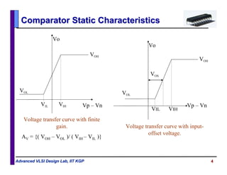
![12Advanced VLSI Design Lab, IIT KGPAdvanced VLSI Design Lab, IIT KGP
M1
M2
Vin+
M3
M4
M5
VDD
VSS
Vbias
Vin-
VDD
M6
M7
Vout
VSS
VSS
Cload
C1
C2
p1 = -1 / {C1 * (gds2 + gds4)}
p2 = -1 / {C2 * (gds6 + gds7)}
Vout = Av (0) * Vin [ 1 + {p2 * exp(-t*p1)} / (p1 – p2) – {p1 * exp(-t*p2)} / (p1 – p2) ]
Frequency Response of The ComparatorFrequency Response of The Comparator](https://image.slidesharecdn.com/comparator-130703043503-phpapp02/85/Comparator-12-320.jpg)


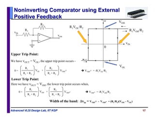

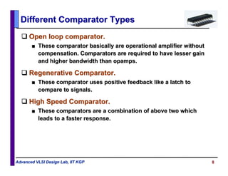
Lower Trip Point:
R1
R1 + R2
VTRP- = VOL
Upper Trip Point:
R1
R1 + R2
VTRP+ = VOH
vIN
vout
VOL
VOH
R1VOL/(R1+R2)
R1VOH/(R1+R2)
vIN vout
R1
R2
Inverting Comparator using ExternalInverting Comparator using External
Positive FeedbackPositive Feedback](https://image.slidesharecdn.com/comparator-130703043503-phpapp02/85/Comparator-18-320.jpg)


This document discusses the design and characteristics of CMOS voltage comparators. It begins by defining the basic requirement of a comparator to compare an analog input voltage to a reference voltage and output a binary signal. It then covers comparator static characteristics like gain, offset voltage, resolution and noise. Dynamic characteristics of propagation delay and slew rate are also discussed. Different comparator circuit topologies like open-loop, regenerative and high-speed designs are presented. The document provides small-signal models of common comparator circuits and examines the effects of hysteresis. It concludes by presenting the typical architecture of high-speed comparators using preamplifier and latch stages to minimize propagation delay.