Download to read offline


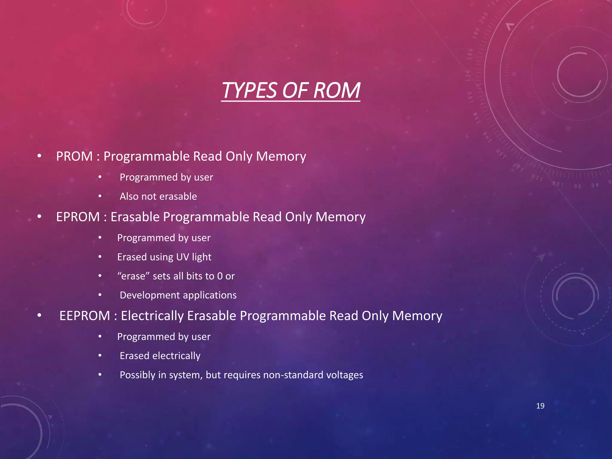
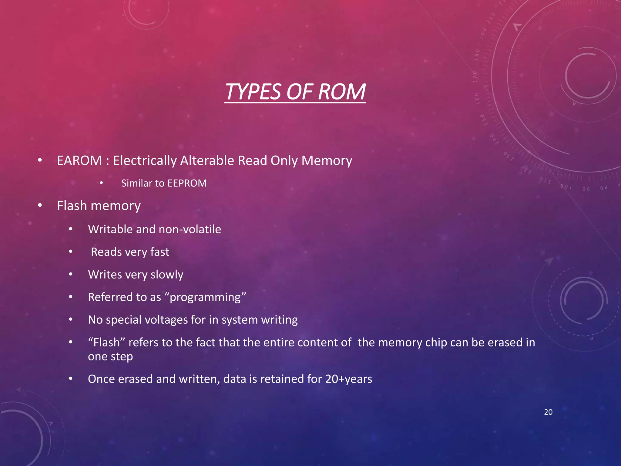


RAM and ROM are two types of computer memory. RAM, or random-access memory, is volatile and used for temporary storage of programs and data that are actively being used. It allows information to be accessed randomly in constant time. ROM, or read-only memory, is non-volatile and used to store permanent programs and data. It can only be modified slowly or with difficulty. The two main types of RAM are SRAM and DRAM, while the main types of ROM include PROM, EPROM, EEPROM, and flash memory. Both RAM and ROM have evolved over time, with innovations allowing for greater memory density, faster speeds, and easier reprogramming.