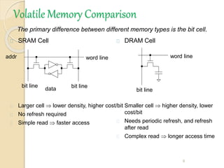
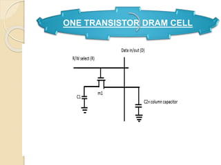
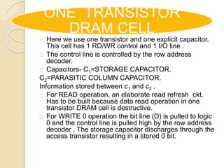
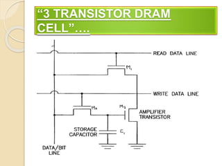
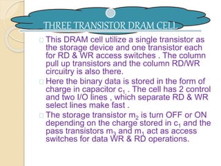
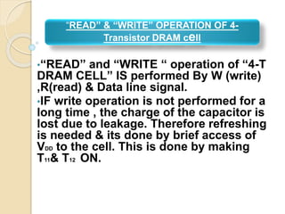
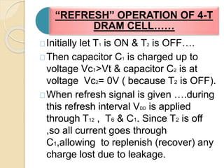
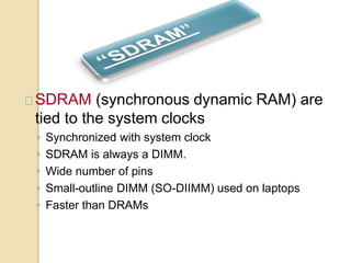
PRESENTATION 
ON 
“DRAM”
(DYNAMIC RANDOM 
ACCESS MEMORY….)
WHY “DRAM”???? 
SRAM , may be volatile to use, but it is not the 
least expensive in significant densities. 
 In SRAM , each bit of memory requires between 4 & 6 
transistors. When millions or billions of bits are required , 
the complexity of all those transistors becomes substantial.
CONCEPTS OF DRAM 
 In DRAM , the binary data is stored as charge in capacitor 
where the presence and absence of charge determines the 
value of stored bit . 
 But data in capacitor cannot be stored for a long time 
because a capacitor holds an electrical charge for a limited 
amt. of time as the charge gradually drains away. 
 DRAM cells require a periodic refreshing of the stored data 
. 
The use of capacitor as the primary storage device 
generally enables the DRAM cell to be realized on a much 
smaller area. 
 Access devices or switches are used for RD/WR 
operations.
KEY FEATURES OF “DRAM” 
A very efficient volatile storage element 
can be created with a capacitor & a 
single transistor , but that capacitor loses 
its contents soon after being charged. 
We need to periodically refresh or 
update each DRAM bit before it 
completely loses its charge. 
A single capacitor takes the place of 
multi-transistor latch. This significant 
reduction in bit complexity makes the 
DRAM more convenient to implement 
main memory in most computers.
The primary difference between different memory types is the bit cell. 
6 
Volatile Memory Comparison 
SRAM Cell 
Larger cell  lower density, higher cost/bit 
No refresh required 
Simple read  faster access 
DRAM Cell 
Smaller cell  higher density, lower 
cost/bit 
Needs periodic refresh, and refresh 
after read 
Complex read  longer access time 
word line 
bit line bit line 
word line 
bit line 
addr 
data
ONE TRANSISTOR DRAM CELL
ONE TRANSISTOR 
DRAM CELL 
Here we use one transistor and one explicit capacitor. 
This cell has 1 RD/WR control and 1 I/O line . 
The control line is controlled by the row address 
decoder. 
Capacitors- C1=STORAGE CAPACITOR. 
C2=PARASITIC COLUMN CAPACITOR. 
Information stored between c1 and c2 . 
For READ operation, an elaborate read refresh ckt. 
Has to be built because data read operation in one 
transistor DRAM cell is destructive. 
For WRITE 0 operation the bit line (D) is pulled to logic 
0 and the control line is pulled high by the row address 
decoder . The storage capacitor discharges through the 
access transistor resulting in a stored 0 bit.
“3 TRANSISTOR DRAM 
CELL”….
THREE TRANSISTOR DRAM CELL 
This DRAM cell utilize a single transistor as 
the storage device and one transistor each 
for RD & WR access switches . The column 
pull up transistors and the column RD/WR 
circuitry is also there. 
Here the binary data is stored in the form of 
charge in capacitor c1 . The cell has 2 control 
and two I/O lines , which separate RD & WR 
select lines make fast . 
The storage transistor m2 is turn OFF or ON 
depending on the charge stored in c1 and the 
pass transistors m3 and m1 act as access 
switches for data WR & RD operations.
“4-TRANSISTOR DRAM CELL”
“READ” & “WRITE” OPERATION OF 4- 
Transistor DRAM cell 
•“READ” and “WRITE “ operation of “4-T 
DRAM CELL” IS performed By W (write) 
,R(read) & Data line signal. 
•IF write operation is not performed for a 
long time , the charge of the capacitor is 
lost due to leakage. Therefore refreshing 
is needed & its done by brief access of 
VDD to the cell. This is done by making 
T11& T12 ON.
OPERATIONS 
TO “READ” A 
DATA BIT 
FROM A DRAM 
STORAGE 
CELL….
1.The sense amplifiers are disconnected. 
2. The bit-lines are precharged to exactly equal voltages that are in 
between high and low logic levels. The bit-lines are physically 
symmetrical to keep the capacitance equal, and therefore the 
voltages are equal. 
3. The precharge circuit is switched off. Because the bit-lines are 
relatively long, they have enough capacitance to maintain the 
precharged voltage for a brief time. This is an example of dynamic 
logic. 
4. The desired row's word-line is then driven high to connect a cell's 
storage capacitor to its bit-line. This causes the transistor to 
conduct, transferring charge between the storage cell and the 
connected bit-line. If the storage cell's capacitor is discharged, it 
will greatly decrease the voltage on the bit-line as the precharge is 
used to charge the storage capacitor. If the storage cell is charged, 
the bit-line's voltage only decreases very slightly. This occurs 
because of the high capacitance of the storage cell capacitor 
compared to the capacitance of the bit-line, thus allowing the 
storage cell to determine the charge level on the bit-line.
5.The sense amplifiers are connected to the bit-lines. Positive 
feedback then occurs from the cross-connected inverters, thereby 
amplifying the small voltage difference between the odd and even 
row bit-lines of a particular column until one bit line is fully at the 
lowest voltage and the other is at the maximum high voltage. Once 
this has happened, the row is "open“. 
6. All storage cells in the open row are sensed simultaneously, and 
the sense amplifier outputs latched. A column address then selects 
which latch bit to connect to the external data bus. Reads of 
different columns in the same row can be performed without a row 
opening delay because, for the open row, all data has already been 
sensed and latched. 
7.While reading of columns in an open row is occurring, current is 
flowing back up the bit-lines from the output of the sense 
amplifiers and recharging the storage cells. This reinforces (i.e. 
"refreshes") the charge in the storage cell by increasing the voltage 
in the storage capacitor if it was charged to begin with, or by 
keeping it discharged if it was empty. Note that due to the length of 
the bit-lines there is a fairly long propagation delay for the charge 
to be transferred back to the cell's capacitor. This takes significant 
time past the end of sense amplification, and thus overlaps with 
one or more column reads.
8.When done with reading all the columns in the current 
open row, the word-line is switched off to disconnect the 
storage cell capacitors (the row is "closed") from the bit-lines. 
The sense amplifier is switched off, and the bit 
lines are precharged again. 
FINISHED WITH 
“READING” 
OPERATION…. 

OPERATION 
TO “WRITE”A 
DATA BIT 
INTO 
MEMORY….
To store data, a row is opened and a given 
column's sense amplifier is temporarily forced to 
the desired high or low voltage state, thus 
causing the bit-line to charge or discharge the cell 
storage capacitor to the desired value. Due to the 
sense amplifier's positive feedback configuration, 
it will hold a bit-line at stable voltage even after 
the forcing voltage is removed. During a write to a 
particular cell, all the columns in a row are sensed 
simultaneously just as during reading, so 
although only a single column's storage-cell 
capacitor charge is changed, the entire row is 
refreshed (written back in).
“REFRESH” OPERATION OF 4-T 
DRAM CELL…… 
Initially let T1 is ON & T2 is OFF…. 
Then capacitor C1 is charged up to 
voltage Vc1>Vt & capacitor C2 is at 
voltage Vc2= 0V ( because T2 is OFF). 
When refresh signal is given ….during 
this refresh interval VDD is applied 
through T12 , T6 & C1. Since T2 is off 
,so all current goes through 
C1,allowing to replenish (recover) any 
charge lost due to leakage.
DIMM (Dual Inline Memory 
Module) 
The 168-pin DIMM is the most popular 
DRAM package in use today 
◦ 144-pin SO-DIMMs (small outline) are used in 
laptops. 
◦ Extra pins to handle functions such as buffering 
and ECC
1.Synchronised DRAM 
(SDRAM). 
2.Rambus DRAM 
(RDRAM).
SDRAM (synchronous dynamic RAM) are 
tied to the system clocks 
◦ Synchronized with system clock 
◦ SDRAM is always a DIMM. 
◦ Wide number of pins 
◦ Small-outline DIMM (SO-DIIMM) used on laptops 
◦ Faster than DRAMs
RDRAM (Rambus DRAM) is a new type 
of RAM 
◦ Speeds of up to 800 MHz 
◦ Comes on sticks called RIMMs 
◦ 184-pin for desktops and 160-pin SO-RIMM 
for laptops
ADVANTAGES OF “DRAM” 
1.LESS POWER DISSIPATION. 
2.HIGH INTEGRATION DENSITY. 
3.LESSER AREA REQUIRED. 
4.LOW COST. 
5.HIGH RELIABILTY.
DISADVANTAGES OF 
“DRAM”…. 
INTERSIGNAL COUPLING.
ANY 
QUERY????
THANK YOU !!!!!  

DRAM

  • 1.
  • 2.
  • 3.
    WHY “DRAM”???? SRAM, may be volatile to use, but it is not the least expensive in significant densities.  In SRAM , each bit of memory requires between 4 & 6 transistors. When millions or billions of bits are required , the complexity of all those transistors becomes substantial.
  • 4.
    CONCEPTS OF DRAM  In DRAM , the binary data is stored as charge in capacitor where the presence and absence of charge determines the value of stored bit .  But data in capacitor cannot be stored for a long time because a capacitor holds an electrical charge for a limited amt. of time as the charge gradually drains away.  DRAM cells require a periodic refreshing of the stored data . The use of capacitor as the primary storage device generally enables the DRAM cell to be realized on a much smaller area.  Access devices or switches are used for RD/WR operations.
  • 5.
    KEY FEATURES OF“DRAM” A very efficient volatile storage element can be created with a capacitor & a single transistor , but that capacitor loses its contents soon after being charged. We need to periodically refresh or update each DRAM bit before it completely loses its charge. A single capacitor takes the place of multi-transistor latch. This significant reduction in bit complexity makes the DRAM more convenient to implement main memory in most computers.
  • 6.
    The primary differencebetween different memory types is the bit cell. 6 Volatile Memory Comparison SRAM Cell Larger cell  lower density, higher cost/bit No refresh required Simple read  faster access DRAM Cell Smaller cell  higher density, lower cost/bit Needs periodic refresh, and refresh after read Complex read  longer access time word line bit line bit line word line bit line addr data
  • 7.
  • 8.
    ONE TRANSISTOR DRAMCELL Here we use one transistor and one explicit capacitor. This cell has 1 RD/WR control and 1 I/O line . The control line is controlled by the row address decoder. Capacitors- C1=STORAGE CAPACITOR. C2=PARASITIC COLUMN CAPACITOR. Information stored between c1 and c2 . For READ operation, an elaborate read refresh ckt. Has to be built because data read operation in one transistor DRAM cell is destructive. For WRITE 0 operation the bit line (D) is pulled to logic 0 and the control line is pulled high by the row address decoder . The storage capacitor discharges through the access transistor resulting in a stored 0 bit.
  • 9.
  • 10.
    THREE TRANSISTOR DRAMCELL This DRAM cell utilize a single transistor as the storage device and one transistor each for RD & WR access switches . The column pull up transistors and the column RD/WR circuitry is also there. Here the binary data is stored in the form of charge in capacitor c1 . The cell has 2 control and two I/O lines , which separate RD & WR select lines make fast . The storage transistor m2 is turn OFF or ON depending on the charge stored in c1 and the pass transistors m3 and m1 act as access switches for data WR & RD operations.
  • 12.
  • 13.
    “READ” & “WRITE”OPERATION OF 4- Transistor DRAM cell •“READ” and “WRITE “ operation of “4-T DRAM CELL” IS performed By W (write) ,R(read) & Data line signal. •IF write operation is not performed for a long time , the charge of the capacitor is lost due to leakage. Therefore refreshing is needed & its done by brief access of VDD to the cell. This is done by making T11& T12 ON.
  • 14.
    OPERATIONS TO “READ”A DATA BIT FROM A DRAM STORAGE CELL….
  • 15.
    1.The sense amplifiersare disconnected. 2. The bit-lines are precharged to exactly equal voltages that are in between high and low logic levels. The bit-lines are physically symmetrical to keep the capacitance equal, and therefore the voltages are equal. 3. The precharge circuit is switched off. Because the bit-lines are relatively long, they have enough capacitance to maintain the precharged voltage for a brief time. This is an example of dynamic logic. 4. The desired row's word-line is then driven high to connect a cell's storage capacitor to its bit-line. This causes the transistor to conduct, transferring charge between the storage cell and the connected bit-line. If the storage cell's capacitor is discharged, it will greatly decrease the voltage on the bit-line as the precharge is used to charge the storage capacitor. If the storage cell is charged, the bit-line's voltage only decreases very slightly. This occurs because of the high capacitance of the storage cell capacitor compared to the capacitance of the bit-line, thus allowing the storage cell to determine the charge level on the bit-line.
  • 16.
    5.The sense amplifiersare connected to the bit-lines. Positive feedback then occurs from the cross-connected inverters, thereby amplifying the small voltage difference between the odd and even row bit-lines of a particular column until one bit line is fully at the lowest voltage and the other is at the maximum high voltage. Once this has happened, the row is "open“. 6. All storage cells in the open row are sensed simultaneously, and the sense amplifier outputs latched. A column address then selects which latch bit to connect to the external data bus. Reads of different columns in the same row can be performed without a row opening delay because, for the open row, all data has already been sensed and latched. 7.While reading of columns in an open row is occurring, current is flowing back up the bit-lines from the output of the sense amplifiers and recharging the storage cells. This reinforces (i.e. "refreshes") the charge in the storage cell by increasing the voltage in the storage capacitor if it was charged to begin with, or by keeping it discharged if it was empty. Note that due to the length of the bit-lines there is a fairly long propagation delay for the charge to be transferred back to the cell's capacitor. This takes significant time past the end of sense amplification, and thus overlaps with one or more column reads.
  • 17.
    8.When done withreading all the columns in the current open row, the word-line is switched off to disconnect the storage cell capacitors (the row is "closed") from the bit-lines. The sense amplifier is switched off, and the bit lines are precharged again. FINISHED WITH “READING” OPERATION…. 
  • 18.
    OPERATION TO “WRITE”A DATA BIT INTO MEMORY….
  • 19.
    To store data,a row is opened and a given column's sense amplifier is temporarily forced to the desired high or low voltage state, thus causing the bit-line to charge or discharge the cell storage capacitor to the desired value. Due to the sense amplifier's positive feedback configuration, it will hold a bit-line at stable voltage even after the forcing voltage is removed. During a write to a particular cell, all the columns in a row are sensed simultaneously just as during reading, so although only a single column's storage-cell capacitor charge is changed, the entire row is refreshed (written back in).
  • 20.
    “REFRESH” OPERATION OF4-T DRAM CELL…… Initially let T1 is ON & T2 is OFF…. Then capacitor C1 is charged up to voltage Vc1>Vt & capacitor C2 is at voltage Vc2= 0V ( because T2 is OFF). When refresh signal is given ….during this refresh interval VDD is applied through T12 , T6 & C1. Since T2 is off ,so all current goes through C1,allowing to replenish (recover) any charge lost due to leakage.
  • 21.
    DIMM (Dual InlineMemory Module) The 168-pin DIMM is the most popular DRAM package in use today ◦ 144-pin SO-DIMMs (small outline) are used in laptops. ◦ Extra pins to handle functions such as buffering and ECC
  • 22.
    1.Synchronised DRAM (SDRAM). 2.Rambus DRAM (RDRAM).
  • 23.
    SDRAM (synchronous dynamicRAM) are tied to the system clocks ◦ Synchronized with system clock ◦ SDRAM is always a DIMM. ◦ Wide number of pins ◦ Small-outline DIMM (SO-DIIMM) used on laptops ◦ Faster than DRAMs
  • 24.
    RDRAM (Rambus DRAM)is a new type of RAM ◦ Speeds of up to 800 MHz ◦ Comes on sticks called RIMMs ◦ 184-pin for desktops and 160-pin SO-RIMM for laptops
  • 25.
    ADVANTAGES OF “DRAM” 1.LESS POWER DISSIPATION. 2.HIGH INTEGRATION DENSITY. 3.LESSER AREA REQUIRED. 4.LOW COST. 5.HIGH RELIABILTY.
  • 26.
    DISADVANTAGES OF “DRAM”…. INTERSIGNAL COUPLING.
  • 27.
  • 28.