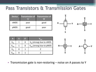
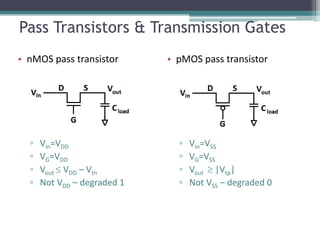
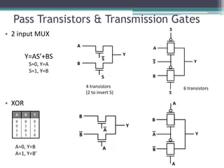
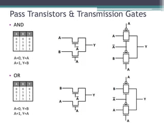
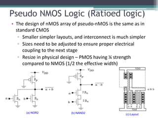
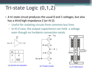
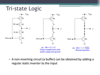
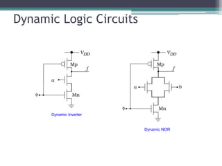
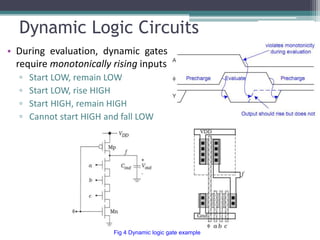
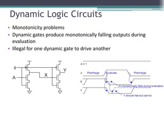
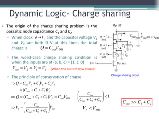
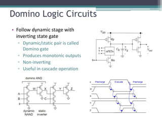
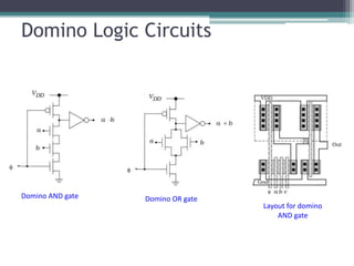
SlideShare a Scribd company logo
Combinational Logic
VLSI Circuit Design
Outline
• Pass Transistors
• Transmission Gates
• Pseudo nMOS Logic
• Tri-state Logic
• Dynamic Logic
• Domino Logic
Pass Transistors & Transmission Gates
• Transmission gate is non-restoring – noise on A passes to Y
Device Transmission of
‘1’
Transmission of
‘0’
nMOS poor good
pMOS good poor
A S S’ Vout
VSS 1 0 VSS (strong) due to nMOS
VDD 1 0 VDD (strong) due to pMOS
VSS 0 1 Z
VDD 0 1 Z
Pass Transistors & Transmission Gates
• nMOS pass transistor
▫ Vin=VDD
▫ VG=VDD
▫ Vout  VDD – Vtn
▫ Not VDD – degraded 1
• pMOS pass transistor
▫ Vin=VSS
▫ VG=VSS
▫ Vout  |Vtp|
▫ Not VSS – degraded 0
Pass Transistors & Transmission Gates
• 2 input MUX
• XOR
A B Y
0
0
1
1
0
1
0
1
0
1
1
0
4 transistors
(2 to invert S)
6 transistors
A=0, Y=B
A=1, Y=B’
Y=AS’+BS
S=0, Y=A
S=1, Y=B
Pass Transistors & Transmission Gates
• AND
• OR
A B Y
0
0
1
1
0
1
0
1
0
0
0
1
A B Y
0
0
1
1
0
1
0
1
0
1
1
1
A=0, Y=A
A=1, Y=B
A=0, Y=B
A=1, Y=A
Pseudo NMOS Logic (Ratioed logic)
• Single PMOS in pull-up network – gate
connected to VSS
• PMOS always in ON state
• Less transistors than CMOS, smaller area
• For N inputs, only requires (N+1) MOS
• NMOS logic array acts as a large switch
between the output f and ground
• However, since the PMOS is always biased
on, VOL can never achieve the ideal value of
0 V – static power dissipation
• A simple inverter using pseudo-NMOS is
shown: Figure 2
Fig 2 Pseudo-nMOS inverter
Fig 1 General structure of a
pseudo-nMOS logic gate
Pseudo NMOS Logic (Ratioed logic)
• The design of nMOS array of pseudo-nMOS is the same as in
standard CMOS
▫ Smaller simpler layouts, and interconnect is much simpler
▫ Sizes need to be adjusted to ensure proper electrical
coupling to the next stage
▫ Resize in physical design – PMOS having ¼ strength
compared to NMOS (1/2 the effective width)
(a) NOR2 (b) NAND2 (c) Layout
Tri-state Logic (0,1,Z)
• A tri-state circuit produces the usual 0 and 1 voltages, but also
has a third high impedance Z (or Hi-Z)
▫ Useful for isolating circuits from common bus lines
▫ In Hi-Z case, the output capacitance can hold a voltage
even though no hardwire connection exists
(a) Symbol and operation (b) Tristate Inverter (c) Tri-state layout
Tri-state Logic
• A non-inverting circuit (a buffer) can be obtained by adding a
regular static inverter to the input
(a) EN = 0, f = Z
Output isolated from both
power supply and ground
(a) EN = 1, f = Data
Normal operation
Dynamic Logic Circuits
• A dynamic logic gate uses clocking and charge
storage properties of MOSFETs to implement
logic operations
▫ Provide a synchronized data flow
▫ Result is valid only for a short period of time
▫ Less transistors, and may be faster than static
cascades
• Based on the circuit in Figure 3
▫ The clock drives a complementary pair of
transistors Mn and Mp
▫ Precharge phase , pMOS is ON, Vout high
▫ Evaluation phase , pMOS is OFF1
0

Figure 3 Basic dynamic logic gateC
Dynamic Logic Circuits
Dynamic Inverter
Dynamic NOR
Dynamic Logic Circuits
• During evaluation, dynamic gates
require monotonically rising inputs
▫ Start LOW, remain LOW
▫ Start LOW, rise HIGH
▫ Start HIGH, remain HIGH
▫ Cannot start HIGH and fall LOW
Fig 4 Dynamic logic gate example
Dynamic Logic Circuits
• Monotonicity problems
• Dynamic gates produce monotonically falling outputs during
evaluation
• Illegal for one dynamic gate to drive another
Dynamic Logic- Charge sharing
• The origin of the charge sharing problem is the
parasitic node capacitance C1 and C2
▫ When clock , and the capacitor voltage V1
and V2 are both 0 V at this time, the total
charge is
▫ The worst-case charge sharing condition is
when the inputs are at (a, b, c) = (1, 1, 0)
▫ The principle of conservation of charge
1
Charge sharing circuit
DDoutVCQ 
fout VVVV  12 (When the current flow ceases)
fout
fffout
VCCC
VCVCVCQ
)( 21
21


DD
out
out
f V
CCC
C
V 







21
1
21






 CCC
C
out
out
DDf VV 
21 CCCout 
DDoutfout VCVCCCQ  )( 21
Domino Logic Circuits
• Follow dynamic stage with
inverting state gate
▫ Dynamic/static pair is called
Domino gate
▫ Produces monotonic outputs
▫ Non-inverting
▫ Useful in cascade operation
Domino Logic Circuits
Layout for domino
AND gate
Domino AND gate Domino OR gate

More Related Content

What's hot

Short Channel Effect In MOSFET
Short Channel Effect In MOSFETShort Channel Effect In MOSFET
Short Channel Effect In MOSFET
Sudhanshu Srivastava
 
CMOS logic circuits
CMOS logic circuitsCMOS logic circuits
CMOS logic circuits
Mahesh_Naidu
 
Synchronization
SynchronizationSynchronization
CMOS Logic
CMOS LogicCMOS Logic
CMOS Topic 5 -_cmos_inverter
CMOS Topic 5 -_cmos_inverterCMOS Topic 5 -_cmos_inverter
CMOS Topic 5 -_cmos_inverter
Ikhwan_Fakrudin
 
MOS transistor 13
MOS transistor 13MOS transistor 13
MOS transistor 13
HIMANSHU DIWAKAR
 
Rc delay modelling in vlsi
Rc delay modelling in vlsiRc delay modelling in vlsi
Rc delay modelling in vlsi
Dr. Vishal Sharma
 
CMOS VLSI design
CMOS VLSI designCMOS VLSI design
CMOS VLSI designRajan Kumar
 
Pass Transistor Logic
Pass Transistor LogicPass Transistor Logic
Pass Transistor Logic
Sudhanshu Janwadkar
 
VLSI Testing Techniques
VLSI Testing TechniquesVLSI Testing Techniques
VLSI Testing Techniques
A B Shinde
 
8251 USART
8251 USART8251 USART
8251 USART
ShivamSood22
 
Vlsi design mosfet
Vlsi design mosfetVlsi design mosfet
Vlsi design mosfetvennila12
 
Microcontroller 8051 and its interfacing
Microcontroller 8051 and its interfacingMicrocontroller 8051 and its interfacing
Microcontroller 8051 and its interfacing
Ankur Mahajan
 
Mosfet
MosfetMosfet
Mosfet
sarunkutti
 
Pipelining approach
Pipelining approachPipelining approach
Pipelining approach
GopinathD17
 
S parameters
S parametersS parameters
S parameters
Amit Rastogi
 
Threshold Voltage & Channel Length Modulation
Threshold Voltage & Channel Length ModulationThreshold Voltage & Channel Length Modulation
Threshold Voltage & Channel Length Modulation
Bulbul Brahma
 
Data types in verilog
Data types in verilogData types in verilog
Data types in verilog
Nallapati Anindra
 

What's hot (20)

Short Channel Effect In MOSFET
Short Channel Effect In MOSFETShort Channel Effect In MOSFET
Short Channel Effect In MOSFET
 
CMOS logic circuits
CMOS logic circuitsCMOS logic circuits
CMOS logic circuits
 
Synchronization
SynchronizationSynchronization
Synchronization
 
CMOS Logic
CMOS LogicCMOS Logic
CMOS Logic
 
CMOS Topic 5 -_cmos_inverter
CMOS Topic 5 -_cmos_inverterCMOS Topic 5 -_cmos_inverter
CMOS Topic 5 -_cmos_inverter
 
MOS transistor 13
MOS transistor 13MOS transistor 13
MOS transistor 13
 
Rc delay modelling in vlsi
Rc delay modelling in vlsiRc delay modelling in vlsi
Rc delay modelling in vlsi
 
CMOS VLSI design
CMOS VLSI designCMOS VLSI design
CMOS VLSI design
 
Pass Transistor Logic
Pass Transistor LogicPass Transistor Logic
Pass Transistor Logic
 
VLSI Testing Techniques
VLSI Testing TechniquesVLSI Testing Techniques
VLSI Testing Techniques
 
8251 USART
8251 USART8251 USART
8251 USART
 
Vlsi design mosfet
Vlsi design mosfetVlsi design mosfet
Vlsi design mosfet
 
n-MOS Fabrication Process
n-MOS Fabrication Processn-MOS Fabrication Process
n-MOS Fabrication Process
 
Microcontroller 8051 and its interfacing
Microcontroller 8051 and its interfacingMicrocontroller 8051 and its interfacing
Microcontroller 8051 and its interfacing
 
Mosfet
MosfetMosfet
Mosfet
 
Pipelining approach
Pipelining approachPipelining approach
Pipelining approach
 
S parameters
S parametersS parameters
S parameters
 
Booth Multiplier
Booth MultiplierBooth Multiplier
Booth Multiplier
 
Threshold Voltage & Channel Length Modulation
Threshold Voltage & Channel Length ModulationThreshold Voltage & Channel Length Modulation
Threshold Voltage & Channel Length Modulation
 
Data types in verilog
Data types in verilogData types in verilog
Data types in verilog
 

Similar to Combinational Logic

circuit families in vlsi.pptx
circuit families in vlsi.pptxcircuit families in vlsi.pptx
circuit families in vlsi.pptx
anitha862251
 
Unit no. 5 cmos logic design
Unit no. 5 cmos logic designUnit no. 5 cmos logic design
Unit no. 5 cmos logic design
swagatkarve
 
CMOS Combinational_Logic_Circuits.pdf
CMOS Combinational_Logic_Circuits.pdfCMOS Combinational_Logic_Circuits.pdf
CMOS Combinational_Logic_Circuits.pdf
SouravRoyElectronics
 
cmoshssd-220105164535.pptx
cmoshssd-220105164535.pptxcmoshssd-220105164535.pptx
cmoshssd-220105164535.pptx
KethavathVenkatesh3
 
CMOS
CMOS CMOS
2. Unit1-CMOS PTL TGL Logic.pdf
2. Unit1-CMOS PTL TGL Logic.pdf2. Unit1-CMOS PTL TGL Logic.pdf
2. Unit1-CMOS PTL TGL Logic.pdf
theanmolchawla19
 
Operational Amplifiers I
Operational Amplifiers IOperational Amplifiers I
Operational Amplifiers I
ali_craigslist
 
vlsi 2 unit.pdfvlsi unit 2 important notes for ece department
vlsi 2 unit.pdfvlsi unit 2 important notes for ece departmentvlsi 2 unit.pdfvlsi unit 2 important notes for ece department
vlsi 2 unit.pdfvlsi unit 2 important notes for ece department
nitcse
 
Lec3 Intro to Computer Engineering by Hsien-Hsin Sean Lee Georgia Tech -- CMO...
Lec3 Intro to Computer Engineering by Hsien-Hsin Sean Lee Georgia Tech -- CMO...Lec3 Intro to Computer Engineering by Hsien-Hsin Sean Lee Georgia Tech -- CMO...
Lec3 Intro to Computer Engineering by Hsien-Hsin Sean Lee Georgia Tech -- CMO...
Hsien-Hsin Sean Lee, Ph.D.
 
CMOS Topic 6 -_designing_combinational_logic_circuits
CMOS Topic 6 -_designing_combinational_logic_circuitsCMOS Topic 6 -_designing_combinational_logic_circuits
CMOS Topic 6 -_designing_combinational_logic_circuits
Ikhwan_Fakrudin
 
Module-2.pptx
Module-2.pptxModule-2.pptx
Module-2.pptx
BEVARAVASUDEVAAP1813
 
presentation on high-performance_dynamic_cmos_circuit
presentation on high-performance_dynamic_cmos_circuitpresentation on high-performance_dynamic_cmos_circuit
presentation on high-performance_dynamic_cmos_circuit
JayminSojitra
 
Hardware combinational
Hardware combinationalHardware combinational
Hardware combinationalDefri Tan
 
VLSI_MOS.pptx
VLSI_MOS.pptxVLSI_MOS.pptx
VLSI_MOS.pptx
VijayRaoKumbhare1
 
VLSI D PPT.pdf
VLSI D PPT.pdfVLSI D PPT.pdf
VLSI D PPT.pdf
AMohan12
 
Ad vlsi pass-transistor logic_yalagoud_patil
Ad vlsi pass-transistor logic_yalagoud_patilAd vlsi pass-transistor logic_yalagoud_patil
Ad vlsi pass-transistor logic_yalagoud_patil
Yalagoud Patil
 
Vlsi gate level design
Vlsi gate level designVlsi gate level design
Vlsi gate level design
CHENCHU CHANDU PRASANTH NADELLA
 
unit4.pdf
unit4.pdfunit4.pdf
unit4.pdf
Arvind72556
 
UNIT - 6.pdf
UNIT - 6.pdfUNIT - 6.pdf
UNIT - 6.pdf
bt2O1O5134KaranGupta
 

Similar to Combinational Logic (20)

circuit families in vlsi.pptx
circuit families in vlsi.pptxcircuit families in vlsi.pptx
circuit families in vlsi.pptx
 
Unit no. 5 cmos logic design
Unit no. 5 cmos logic designUnit no. 5 cmos logic design
Unit no. 5 cmos logic design
 
CMOS Combinational_Logic_Circuits.pdf
CMOS Combinational_Logic_Circuits.pdfCMOS Combinational_Logic_Circuits.pdf
CMOS Combinational_Logic_Circuits.pdf
 
cmoshssd-220105164535.pptx
cmoshssd-220105164535.pptxcmoshssd-220105164535.pptx
cmoshssd-220105164535.pptx
 
CMOS
CMOS CMOS
CMOS
 
2. Unit1-CMOS PTL TGL Logic.pdf
2. Unit1-CMOS PTL TGL Logic.pdf2. Unit1-CMOS PTL TGL Logic.pdf
2. Unit1-CMOS PTL TGL Logic.pdf
 
Operational Amplifiers I
Operational Amplifiers IOperational Amplifiers I
Operational Amplifiers I
 
vlsi 2 unit.pdfvlsi unit 2 important notes for ece department
vlsi 2 unit.pdfvlsi unit 2 important notes for ece departmentvlsi 2 unit.pdfvlsi unit 2 important notes for ece department
vlsi 2 unit.pdfvlsi unit 2 important notes for ece department
 
Lec3 Intro to Computer Engineering by Hsien-Hsin Sean Lee Georgia Tech -- CMO...
Lec3 Intro to Computer Engineering by Hsien-Hsin Sean Lee Georgia Tech -- CMO...Lec3 Intro to Computer Engineering by Hsien-Hsin Sean Lee Georgia Tech -- CMO...
Lec3 Intro to Computer Engineering by Hsien-Hsin Sean Lee Georgia Tech -- CMO...
 
CMOS Topic 6 -_designing_combinational_logic_circuits
CMOS Topic 6 -_designing_combinational_logic_circuitsCMOS Topic 6 -_designing_combinational_logic_circuits
CMOS Topic 6 -_designing_combinational_logic_circuits
 
Module-2.pptx
Module-2.pptxModule-2.pptx
Module-2.pptx
 
presentation on high-performance_dynamic_cmos_circuit
presentation on high-performance_dynamic_cmos_circuitpresentation on high-performance_dynamic_cmos_circuit
presentation on high-performance_dynamic_cmos_circuit
 
Chapter 10
Chapter 10Chapter 10
Chapter 10
 
Hardware combinational
Hardware combinationalHardware combinational
Hardware combinational
 
VLSI_MOS.pptx
VLSI_MOS.pptxVLSI_MOS.pptx
VLSI_MOS.pptx
 
VLSI D PPT.pdf
VLSI D PPT.pdfVLSI D PPT.pdf
VLSI D PPT.pdf
 
Ad vlsi pass-transistor logic_yalagoud_patil
Ad vlsi pass-transistor logic_yalagoud_patilAd vlsi pass-transistor logic_yalagoud_patil
Ad vlsi pass-transistor logic_yalagoud_patil
 
Vlsi gate level design
Vlsi gate level designVlsi gate level design
Vlsi gate level design
 
unit4.pdf
unit4.pdfunit4.pdf
unit4.pdf
 
UNIT - 6.pdf
UNIT - 6.pdfUNIT - 6.pdf
UNIT - 6.pdf
 

More from Sirat Mahmood

Vlsi circuit design
Vlsi circuit designVlsi circuit design
Vlsi circuit design
Sirat Mahmood
 
Vlsi circuit design 2
Vlsi circuit design  2Vlsi circuit design  2
Vlsi circuit design 2
Sirat Mahmood
 
Video and sound
Video and soundVideo and sound
Video and sound
Sirat Mahmood
 
Transforming data into information
Transforming data into informationTransforming data into information
Transforming data into information
Sirat Mahmood
 
The basics of information systems
The basics of information systemsThe basics of information systems
The basics of information systems
Sirat Mahmood
 
Synchronous motor
Synchronous motorSynchronous motor
Synchronous motor
Sirat Mahmood
 
Symmetrical components
Symmetrical componentsSymmetrical components
Symmetrical components
Sirat Mahmood
 
Single phase induction motor
Single phase induction motorSingle phase induction motor
Single phase induction motor
Sirat Mahmood
 
Semiconductor diodes1
Semiconductor diodes1Semiconductor diodes1
Semiconductor diodes1
Sirat Mahmood
 
Semiconductor diodes
Semiconductor diodesSemiconductor diodes
Semiconductor diodes
Sirat Mahmood
 
Nuclear power station
Nuclear power stationNuclear power station
Nuclear power station
Sirat Mahmood
 
Network basics
Network basicsNetwork basics
Network basics
Sirat Mahmood
 
Mosfet
MosfetMosfet
Modern cpus
Modern cpusModern cpus
Modern cpus
Sirat Mahmood
 
Introducing computer systems
Introducing computer systemsIntroducing computer systems
Introducing computer systems
Sirat Mahmood
 
Infrared & Thermal Testing
 Infrared & Thermal Testing Infrared & Thermal Testing
Infrared & Thermal Testing
Sirat Mahmood
 
Engineering drawing
Engineering drawingEngineering drawing
Engineering drawing
Sirat Mahmood
 
Station Performance and Operation Characteristics
Station Performance and Operation Characteristics Station Performance and Operation Characteristics
Station Performance and Operation Characteristics
Sirat Mahmood
 
Defects in Materials
Defects in MaterialsDefects in Materials
Defects in Materials
Sirat Mahmood
 
Condition Monitoring Technology
Condition Monitoring Technology Condition Monitoring Technology
Condition Monitoring Technology
Sirat Mahmood
 

More from Sirat Mahmood (20)

Vlsi circuit design
Vlsi circuit designVlsi circuit design
Vlsi circuit design
 
Vlsi circuit design 2
Vlsi circuit design  2Vlsi circuit design  2
Vlsi circuit design 2
 
Video and sound
Video and soundVideo and sound
Video and sound
 
Transforming data into information
Transforming data into informationTransforming data into information
Transforming data into information
 
The basics of information systems
The basics of information systemsThe basics of information systems
The basics of information systems
 
Synchronous motor
Synchronous motorSynchronous motor
Synchronous motor
 
Symmetrical components
Symmetrical componentsSymmetrical components
Symmetrical components
 
Single phase induction motor
Single phase induction motorSingle phase induction motor
Single phase induction motor
 
Semiconductor diodes1
Semiconductor diodes1Semiconductor diodes1
Semiconductor diodes1
 
Semiconductor diodes
Semiconductor diodesSemiconductor diodes
Semiconductor diodes
 
Nuclear power station
Nuclear power stationNuclear power station
Nuclear power station
 
Network basics
Network basicsNetwork basics
Network basics
 
Mosfet
MosfetMosfet
Mosfet
 
Modern cpus
Modern cpusModern cpus
Modern cpus
 
Introducing computer systems
Introducing computer systemsIntroducing computer systems
Introducing computer systems
 
Infrared & Thermal Testing
 Infrared & Thermal Testing Infrared & Thermal Testing
Infrared & Thermal Testing
 
Engineering drawing
Engineering drawingEngineering drawing
Engineering drawing
 
Station Performance and Operation Characteristics
Station Performance and Operation Characteristics Station Performance and Operation Characteristics
Station Performance and Operation Characteristics
 
Defects in Materials
Defects in MaterialsDefects in Materials
Defects in Materials
 
Condition Monitoring Technology
Condition Monitoring Technology Condition Monitoring Technology
Condition Monitoring Technology
 

Recently uploaded

road safety engineering r s e unit 3.pdf
road safety engineering  r s e unit 3.pdfroad safety engineering  r s e unit 3.pdf
road safety engineering r s e unit 3.pdf
VENKATESHvenky89705
 
Final project report on grocery store management system..pdf
Final project report on grocery store management system..pdfFinal project report on grocery store management system..pdf
Final project report on grocery store management system..pdf
Kamal Acharya
 
Investor-Presentation-Q1FY2024 investor presentation document.pptx
Investor-Presentation-Q1FY2024 investor presentation document.pptxInvestor-Presentation-Q1FY2024 investor presentation document.pptx
Investor-Presentation-Q1FY2024 investor presentation document.pptx
AmarGB2
 
CME397 Surface Engineering- Professional Elective
CME397 Surface Engineering- Professional ElectiveCME397 Surface Engineering- Professional Elective
CME397 Surface Engineering- Professional Elective
karthi keyan
 
weather web application report.pdf
weather web application report.pdfweather web application report.pdf
weather web application report.pdf
Pratik Pawar
 
AKS UNIVERSITY Satna Final Year Project By OM Hardaha.pdf
AKS UNIVERSITY Satna Final Year Project By OM Hardaha.pdfAKS UNIVERSITY Satna Final Year Project By OM Hardaha.pdf
AKS UNIVERSITY Satna Final Year Project By OM Hardaha.pdf
SamSarthak3
 
Hierarchical Digital Twin of a Naval Power System
Hierarchical Digital Twin of a Naval Power SystemHierarchical Digital Twin of a Naval Power System
Hierarchical Digital Twin of a Naval Power System
Kerry Sado
 
14 Template Contractual Notice - EOT Application
14 Template Contractual Notice - EOT Application14 Template Contractual Notice - EOT Application
14 Template Contractual Notice - EOT Application
SyedAbiiAzazi1
 
English lab ppt no titlespecENG PPTt.pdf
English lab ppt no titlespecENG PPTt.pdfEnglish lab ppt no titlespecENG PPTt.pdf
English lab ppt no titlespecENG PPTt.pdf
BrazilAccount1
 
Standard Reomte Control Interface - Neometrix
Standard Reomte Control Interface - NeometrixStandard Reomte Control Interface - Neometrix
Standard Reomte Control Interface - Neometrix
Neometrix_Engineering_Pvt_Ltd
 
一比一原版(IIT毕业证)伊利诺伊理工大学毕业证成绩单专业办理
一比一原版(IIT毕业证)伊利诺伊理工大学毕业证成绩单专业办理一比一原版(IIT毕业证)伊利诺伊理工大学毕业证成绩单专业办理
一比一原版(IIT毕业证)伊利诺伊理工大学毕业证成绩单专业办理
zwunae
 
Nuclear Power Economics and Structuring 2024
Nuclear Power Economics and Structuring 2024Nuclear Power Economics and Structuring 2024
Nuclear Power Economics and Structuring 2024
Massimo Talia
 
AP LAB PPT.pdf ap lab ppt no title specific
AP LAB PPT.pdf ap lab ppt no title specificAP LAB PPT.pdf ap lab ppt no title specific
AP LAB PPT.pdf ap lab ppt no title specific
BrazilAccount1
 
space technology lecture notes on satellite
space technology lecture notes on satellitespace technology lecture notes on satellite
space technology lecture notes on satellite
ongomchris
 
Gen AI Study Jams _ For the GDSC Leads in India.pdf
Gen AI Study Jams _ For the GDSC Leads in India.pdfGen AI Study Jams _ For the GDSC Leads in India.pdf
Gen AI Study Jams _ For the GDSC Leads in India.pdf
gdsczhcet
 
NUMERICAL SIMULATIONS OF HEAT AND MASS TRANSFER IN CONDENSING HEAT EXCHANGERS...
NUMERICAL SIMULATIONS OF HEAT AND MASS TRANSFER IN CONDENSING HEAT EXCHANGERS...NUMERICAL SIMULATIONS OF HEAT AND MASS TRANSFER IN CONDENSING HEAT EXCHANGERS...
NUMERICAL SIMULATIONS OF HEAT AND MASS TRANSFER IN CONDENSING HEAT EXCHANGERS...
ssuser7dcef0
 
在线办理(ANU毕业证书)澳洲国立大学毕业证录取通知书一模一样
在线办理(ANU毕业证书)澳洲国立大学毕业证录取通知书一模一样在线办理(ANU毕业证书)澳洲国立大学毕业证录取通知书一模一样
在线办理(ANU毕业证书)澳洲国立大学毕业证录取通知书一模一样
obonagu
 
Sachpazis:Terzaghi Bearing Capacity Estimation in simple terms with Calculati...
Sachpazis:Terzaghi Bearing Capacity Estimation in simple terms with Calculati...Sachpazis:Terzaghi Bearing Capacity Estimation in simple terms with Calculati...
Sachpazis:Terzaghi Bearing Capacity Estimation in simple terms with Calculati...
Dr.Costas Sachpazis
 
Planning Of Procurement o different goods and services
Planning Of Procurement o different goods and servicesPlanning Of Procurement o different goods and services
Planning Of Procurement o different goods and services
JoytuBarua2
 
Immunizing Image Classifiers Against Localized Adversary Attacks
Immunizing Image Classifiers Against Localized Adversary AttacksImmunizing Image Classifiers Against Localized Adversary Attacks
Immunizing Image Classifiers Against Localized Adversary Attacks
gerogepatton
 

Recently uploaded (20)

road safety engineering r s e unit 3.pdf
road safety engineering  r s e unit 3.pdfroad safety engineering  r s e unit 3.pdf
road safety engineering r s e unit 3.pdf
 
Final project report on grocery store management system..pdf
Final project report on grocery store management system..pdfFinal project report on grocery store management system..pdf
Final project report on grocery store management system..pdf
 
Investor-Presentation-Q1FY2024 investor presentation document.pptx
Investor-Presentation-Q1FY2024 investor presentation document.pptxInvestor-Presentation-Q1FY2024 investor presentation document.pptx
Investor-Presentation-Q1FY2024 investor presentation document.pptx
 
CME397 Surface Engineering- Professional Elective
CME397 Surface Engineering- Professional ElectiveCME397 Surface Engineering- Professional Elective
CME397 Surface Engineering- Professional Elective
 
weather web application report.pdf
weather web application report.pdfweather web application report.pdf
weather web application report.pdf
 
AKS UNIVERSITY Satna Final Year Project By OM Hardaha.pdf
AKS UNIVERSITY Satna Final Year Project By OM Hardaha.pdfAKS UNIVERSITY Satna Final Year Project By OM Hardaha.pdf
AKS UNIVERSITY Satna Final Year Project By OM Hardaha.pdf
 
Hierarchical Digital Twin of a Naval Power System
Hierarchical Digital Twin of a Naval Power SystemHierarchical Digital Twin of a Naval Power System
Hierarchical Digital Twin of a Naval Power System
 
14 Template Contractual Notice - EOT Application
14 Template Contractual Notice - EOT Application14 Template Contractual Notice - EOT Application
14 Template Contractual Notice - EOT Application
 
English lab ppt no titlespecENG PPTt.pdf
English lab ppt no titlespecENG PPTt.pdfEnglish lab ppt no titlespecENG PPTt.pdf
English lab ppt no titlespecENG PPTt.pdf
 
Standard Reomte Control Interface - Neometrix
Standard Reomte Control Interface - NeometrixStandard Reomte Control Interface - Neometrix
Standard Reomte Control Interface - Neometrix
 
一比一原版(IIT毕业证)伊利诺伊理工大学毕业证成绩单专业办理
一比一原版(IIT毕业证)伊利诺伊理工大学毕业证成绩单专业办理一比一原版(IIT毕业证)伊利诺伊理工大学毕业证成绩单专业办理
一比一原版(IIT毕业证)伊利诺伊理工大学毕业证成绩单专业办理
 
Nuclear Power Economics and Structuring 2024
Nuclear Power Economics and Structuring 2024Nuclear Power Economics and Structuring 2024
Nuclear Power Economics and Structuring 2024
 
AP LAB PPT.pdf ap lab ppt no title specific
AP LAB PPT.pdf ap lab ppt no title specificAP LAB PPT.pdf ap lab ppt no title specific
AP LAB PPT.pdf ap lab ppt no title specific
 
space technology lecture notes on satellite
space technology lecture notes on satellitespace technology lecture notes on satellite
space technology lecture notes on satellite
 
Gen AI Study Jams _ For the GDSC Leads in India.pdf
Gen AI Study Jams _ For the GDSC Leads in India.pdfGen AI Study Jams _ For the GDSC Leads in India.pdf
Gen AI Study Jams _ For the GDSC Leads in India.pdf
 
NUMERICAL SIMULATIONS OF HEAT AND MASS TRANSFER IN CONDENSING HEAT EXCHANGERS...
NUMERICAL SIMULATIONS OF HEAT AND MASS TRANSFER IN CONDENSING HEAT EXCHANGERS...NUMERICAL SIMULATIONS OF HEAT AND MASS TRANSFER IN CONDENSING HEAT EXCHANGERS...
NUMERICAL SIMULATIONS OF HEAT AND MASS TRANSFER IN CONDENSING HEAT EXCHANGERS...
 
在线办理(ANU毕业证书)澳洲国立大学毕业证录取通知书一模一样
在线办理(ANU毕业证书)澳洲国立大学毕业证录取通知书一模一样在线办理(ANU毕业证书)澳洲国立大学毕业证录取通知书一模一样
在线办理(ANU毕业证书)澳洲国立大学毕业证录取通知书一模一样
 
Sachpazis:Terzaghi Bearing Capacity Estimation in simple terms with Calculati...
Sachpazis:Terzaghi Bearing Capacity Estimation in simple terms with Calculati...Sachpazis:Terzaghi Bearing Capacity Estimation in simple terms with Calculati...
Sachpazis:Terzaghi Bearing Capacity Estimation in simple terms with Calculati...
 
Planning Of Procurement o different goods and services
Planning Of Procurement o different goods and servicesPlanning Of Procurement o different goods and services
Planning Of Procurement o different goods and services
 
Immunizing Image Classifiers Against Localized Adversary Attacks
Immunizing Image Classifiers Against Localized Adversary AttacksImmunizing Image Classifiers Against Localized Adversary Attacks
Immunizing Image Classifiers Against Localized Adversary Attacks
 

Combinational Logic

  • 2. Outline • Pass Transistors • Transmission Gates • Pseudo nMOS Logic • Tri-state Logic • Dynamic Logic • Domino Logic
  • 3. Pass Transistors & Transmission Gates • Transmission gate is non-restoring – noise on A passes to Y Device Transmission of ‘1’ Transmission of ‘0’ nMOS poor good pMOS good poor A S S’ Vout VSS 1 0 VSS (strong) due to nMOS VDD 1 0 VDD (strong) due to pMOS VSS 0 1 Z VDD 0 1 Z
  • 4. Pass Transistors & Transmission Gates • nMOS pass transistor ▫ Vin=VDD ▫ VG=VDD ▫ Vout  VDD – Vtn ▫ Not VDD – degraded 1 • pMOS pass transistor ▫ Vin=VSS ▫ VG=VSS ▫ Vout  |Vtp| ▫ Not VSS – degraded 0
  • 5. Pass Transistors & Transmission Gates • 2 input MUX • XOR A B Y 0 0 1 1 0 1 0 1 0 1 1 0 4 transistors (2 to invert S) 6 transistors A=0, Y=B A=1, Y=B’ Y=AS’+BS S=0, Y=A S=1, Y=B
  • 6. Pass Transistors & Transmission Gates • AND • OR A B Y 0 0 1 1 0 1 0 1 0 0 0 1 A B Y 0 0 1 1 0 1 0 1 0 1 1 1 A=0, Y=A A=1, Y=B A=0, Y=B A=1, Y=A
  • 7. Pseudo NMOS Logic (Ratioed logic) • Single PMOS in pull-up network – gate connected to VSS • PMOS always in ON state • Less transistors than CMOS, smaller area • For N inputs, only requires (N+1) MOS • NMOS logic array acts as a large switch between the output f and ground • However, since the PMOS is always biased on, VOL can never achieve the ideal value of 0 V – static power dissipation • A simple inverter using pseudo-NMOS is shown: Figure 2 Fig 2 Pseudo-nMOS inverter Fig 1 General structure of a pseudo-nMOS logic gate
  • 8. Pseudo NMOS Logic (Ratioed logic) • The design of nMOS array of pseudo-nMOS is the same as in standard CMOS ▫ Smaller simpler layouts, and interconnect is much simpler ▫ Sizes need to be adjusted to ensure proper electrical coupling to the next stage ▫ Resize in physical design – PMOS having ¼ strength compared to NMOS (1/2 the effective width) (a) NOR2 (b) NAND2 (c) Layout
  • 9. Tri-state Logic (0,1,Z) • A tri-state circuit produces the usual 0 and 1 voltages, but also has a third high impedance Z (or Hi-Z) ▫ Useful for isolating circuits from common bus lines ▫ In Hi-Z case, the output capacitance can hold a voltage even though no hardwire connection exists (a) Symbol and operation (b) Tristate Inverter (c) Tri-state layout
  • 10. Tri-state Logic • A non-inverting circuit (a buffer) can be obtained by adding a regular static inverter to the input (a) EN = 0, f = Z Output isolated from both power supply and ground (a) EN = 1, f = Data Normal operation
  • 11. Dynamic Logic Circuits • A dynamic logic gate uses clocking and charge storage properties of MOSFETs to implement logic operations ▫ Provide a synchronized data flow ▫ Result is valid only for a short period of time ▫ Less transistors, and may be faster than static cascades • Based on the circuit in Figure 3 ▫ The clock drives a complementary pair of transistors Mn and Mp ▫ Precharge phase , pMOS is ON, Vout high ▫ Evaluation phase , pMOS is OFF1 0  Figure 3 Basic dynamic logic gateC
  • 12. Dynamic Logic Circuits Dynamic Inverter Dynamic NOR
  • 13. Dynamic Logic Circuits • During evaluation, dynamic gates require monotonically rising inputs ▫ Start LOW, remain LOW ▫ Start LOW, rise HIGH ▫ Start HIGH, remain HIGH ▫ Cannot start HIGH and fall LOW Fig 4 Dynamic logic gate example
  • 14. Dynamic Logic Circuits • Monotonicity problems • Dynamic gates produce monotonically falling outputs during evaluation • Illegal for one dynamic gate to drive another
  • 15. Dynamic Logic- Charge sharing • The origin of the charge sharing problem is the parasitic node capacitance C1 and C2 ▫ When clock , and the capacitor voltage V1 and V2 are both 0 V at this time, the total charge is ▫ The worst-case charge sharing condition is when the inputs are at (a, b, c) = (1, 1, 0) ▫ The principle of conservation of charge 1 Charge sharing circuit DDoutVCQ  fout VVVV  12 (When the current flow ceases) fout fffout VCCC VCVCVCQ )( 21 21   DD out out f V CCC C V         21 1 21        CCC C out out DDf VV  21 CCCout  DDoutfout VCVCCCQ  )( 21
  • 16. Domino Logic Circuits • Follow dynamic stage with inverting state gate ▫ Dynamic/static pair is called Domino gate ▫ Produces monotonic outputs ▫ Non-inverting ▫ Useful in cascade operation
  • 17. Domino Logic Circuits Layout for domino AND gate Domino AND gate Domino OR gate