SlideShare a Scribd company logo
SEQUENTIAL CIRCUITS I
i1
in
o1
om
Combinational
Circuit
I1
Ik
O1
Ok
State of circuit = content of k memory cells.
One bit (0 or 1) per cell → 2k possible states
Actual state is I1, . . . , Ik
Next state is O1, . . . , Ok
oi = f(i1, . . . , in, I1, . . . , Ik), 1 ≤ i ≤ m
Oj = f(i1, . . . , in, I1, . . . , Ik), 1 ≤ j ≤ k
A sequential circuit is in a stable state when Ij = Oj for
j = 1, . . . , k
1
Asynchronous Sequential Circuits
Responds to a change in one of the inputs
Input signals change one at a time and only when the
circuit is in a stable state
Memory elements = Latches: Two-state circuit
that stores one bit
SR latch: 2 inputs (S)et, (R)eset, and 2 outputs Q, Q̄
Its equations are:
Q = R + p = R̄p̄
P = S + q = S̄q̄
where p, q are the actual states and Q, P are the next
states (with P = Q̄)
2
Stable States of SR Latch
To find the stable states
• Obtain truth table of SR latch according to Q =
f(q, p, R, S) = R̄p̄
P = f(q, p, R, S) = S̄q̄
• Build a K-map with values of Q,P as entries
• Circle entries where Q,P = q,p
q p R S Q P
0 0 0 0 1 1
0 0 0 1 1 0
0 0 1 0 0 1
0 0 1 1 0 0
0 1 0 0 0 1
0 1 0 1 0 0
0 1 1 0 0 1
0 1 1 1 0 0
1 0 0 0 1 0
1 0 0 1 1 0
1 0 1 0 0 0
1 0 1 1 0 0
1 1 0 0 0 0
1 1 0 1 0 0
1 1 1 0 0 0
1 1 1 1 0 0
7→
00 01 11 10
00 11 10 00 01
01 01 00 00 01
11 00 00 00 00
10 10 10 00 00
3
Functionality of SR Latch
(continued)
S,R = 1,1 7→ stable state Q,Q̄ = 0,0 → Q = Q̄
→ undefined state. We must avoid inputs
S,R = 1,1 simultaneously
Q,Q̄ = 0,0 7→ indeterminate next state when S,R
becomes 0,0 simultaneously.
00 01 11 10
00 11 10 00 01
01 01 00 00 01
11 00 00 00 00
10 10 10 00 00
S,R = 1,0 7→ set state Q,Q̄ = 1,0
S,R = 0,1 7→ reset state Q,Q̄ = 0,1
S,R = 0,0 7→ next state = actual state of Q,Q̄
4
Functionality of SR Latch
(continued)
S,R = 0,0 S,R = 0,1
00 01 11 10
00 11 10 00 01
01 01 00 00 01
11 00 00 00 00
10 10 10 00 00
00 01 11 10
00 11 10 00 01
01 01 00 00 01
11 00 00 00 00
10 10 10 00 00
S,R = 1,0 S,R = 1,1
00 01 11 10
00 11 10 00 01
01 01 00 00 01
11 00 00 00 00
10 10 10 00 00
00 01 11 10
00 11 10 00 01
01 01 00 00 01
11 00 00 00 00
10 10 10 00 00
Therefore the truth table of SR latch is
5
SR Latch
(equivalent representation)
S
R
Q
q
Its equation is Q = SR̄ + qR̄
Truth table and transition table below
q R S Q
0 0 0 0
0 0 1 1
0 1 0 0
0 1 1 0
1 0 0 1
1 0 1 1
1 1 0 0
1 1 1 0
7→
00 01 11 10
0 0 1 X 0
0 1 1 X 0
⇒ if SR = 0 (S,R 6= 1,1) then
minimal → Q = S + R̄q
6
S̄R̄ Latch
Uses NAND gates
⇓
When S̄R̄ = 0, that is S,R 6= 0,0 then its
equation is
Q = S̄ + Rq
7
Synchronous Sequential Circuits
Responds to a clock pulse
State transitions occurs only at fixed time intervals dic-
tated by the clock pulses.
Time is discrete: the next state can be described at
time t + 1 with respect to the actual state at time t
More complex design but more reliable than asynchronous
circuits.
Memory elements = Flip-flops: Two-state circuit that
stores one bit
8
SR Flip-Flop
S
C
R
Q
Q’
→
Qt S R Qt+1
0 0 0 0
0 0 1 0
0 1 0 1
0 1 1 ?
1 0 0 1
1 0 1 0
1 1 0 1
1 1 1 ?
Working conditions: SR = 0. Pulse triggered flip-flop
Characteristic equation: (after simplification)
Qt+1 = S + R̄Qt
Characteristic table
S R Qt+1 Operation
0 0 Qt No change
0 1 0 Reset
1 0 1 Set
1 1 ? Undefined
Excitation table
Qt Qt+1 S R
0 0 0 X
0 1 1 0
1 0 0 1
1 1 X 0
9
D Flip-Flop
C
Q
Q’
D
→
Qt D Qt+1
0 0 0
0 1 1
1 0 0
1 1 1
Working conditions: No undefined state. Edge
triggered flip-flop
Characteristic equation: (after simplification)
Qt+1 = D
Characteristic table
D Qt+1 Operation
0 0 Reset
1 1 Set
Excitation table
Qt Qt+1 D
0 0 0
0 1 1
1 0 0
1 1 1
10
JK Flip-Flop
K
C
J
Q
Q’
→
Qt J K Qt+1
0 0 0 0
0 0 1 0
0 1 0 1
0 1 1 1
1 0 0 1
1 0 1 0
1 1 0 1
1 1 1 0
Working conditions: No undefined state. Pulse or edge
triggered flip-flop
Characteristic equation: (after simplification)
Qt+1 = JQ̄ + K̄Q
Characteristic table
J K Qt+1 Operation
0 0 Qt No change
0 1 0 Reset
1 0 1 Set
1 1 Q̄t Complement
Excitation table
Qt Qt+1 J K
0 0 0 X
0 1 1 X
1 0 X 1
1 1 X 0
11
T Flip-Flop
Q
Q’
C
T →
Qt T Qt+1
0 0 0
0 1 1
1 0 1
1 1 0
Working conditions: No undefined state. Pulse or edge
triggered flip-flop
Characteristic equation: (after simplification)
Qt+1 = TQ̄ + T̄Q
Characteristic table
T Qt+1 Operation
0 Qt Reset
1 Q̄t Set
Excitation table
Qt Qt+1 T
0 0 0
0 1 1
1 0 1
1 1 0
12
Standard Graphics Symbols for
Latches and Flip-Flops
13
Synchronous Sequential Circuit Analysis
Given a synchronous sequential circuit, example
We can express its behavior in three ways: by
1. Circuit output functions and flip-flops input
functions
2. Circuit output functions and state equations
3. State table and state diagram
14
Synchronous Sequential Circuit Analysis
(Circuit output and flip-flops input functions)
Question: What are the values of Y , DA and DB ?
Use the information contained in the combinational cir-
cuit to obtain the circuit’s outputs and the flip-flops’
inputs. That is
• Y = X̄(At + Bt)
• DA = X(At + Bt)
• DB = XĀt
Thus we can represent the states changes and the out-
puts. However, this representation is quite useless;
we still do not know what the circuit truly does (par-
ticularly when we do not know the types of flip-flops
used). The following two representations are better.
15
Synchronous Sequential Circuit Analysis
(Circuit output functions and state equations)
Question: Values of Y , At+1 and Bt+1 ?
For circuit’s output functions: use the information con-
tained in the combinational circuit. That is
• Y = X̄(At + Bt)
For flip-flops’ state equations: either
• Make a truth table and minimize to obtain the
state equations. Or,
• Substitute the flip-flops’ input functions into the
flip-flops’ characteristic equations to obtain the
state equations
The characteristic equation of D flip-flop is
Qt+1 = D, therefore
• At+1 = DA = X(At + Bt)
• Bt+1 = DB = XĀt
16
Synchronous Sequential Circuit Analysis
(State table and state diagram)
Question: What are the ouputs and next states given
the inputs and current states?
State table: Enumerates the functional relationships be-
tween inputs, outputs, and states flip-flops states of
a sequential circuit
State diagram: Graphical representation of a state ta-
ble
For each possible (actual) state of the circuit and for
each possible combination of values of input vari-
ables:
1. Use the flip-flops’ input functions and their char-
acteristic tables to determine the next state of the
circuit (A,B in example)
2. Use the circuit’s output functions to determine
the output values (Y in example)
17
Synchronous Sequential Circuit Analysis
(State table and state diagram)
(continued)
State Table
Present state Next state Output
X = 0 X = 1 X = 0 X = 1
A B A B A B Y Y
0 0 0 0 0 1 0 0
0 1 0 0 1 1 1 0
1 0 0 0 1 0 1 0
1 1 0 0 1 0 1 0
State Diagram
18
Synchronous Sequential Circuit Design
1. Obtain state table from circuit specification (state
diagram, state equations or timing diagram)
2. If necessary, assign binary codes to each state of
state table
3. Determine the number and type of flip-flops needed
and assign a letter to each
4. From the state table, derive the circuit excitation
and output tables
5. Using K-maps, derive the circuit output functions
and the flip-flops input functions
6. Draw the synchronous sequential logic circuit
19
Synchronous Sequential Circuit Design
(Example)
Given the
State diagram
or the
State equations
Y = AtBt + X
At+1 = AtB̄t + BtX̄
Bt+1 = AtBtX̄ + Ātx + B̄tX
of a synchronous sequential circuit specification
Then . . .
. . . use the following design method . . .
20
Synchronous Sequential Circuit Design
(continued)
Step 1:
Present state Next state Output
X = 0 X = 1 X = 0 X = 1
A B A B A B Y Y
0 0 0 0 0 1 0 0
0 1 1 0 0 1 0 1
1 0 1 0 1 1 0 1
1 1 1 1 0 0 1 1
Step 2: Not necessary in our example
Step 3:
Type of flip-flop is usually given. If not, then select
cheapest: in general JK flip-flop
Number of flip-flops depends on number of states
and the encoding used. In our case we need 2 flip-
flops since there are 4 states (2 = log2 4), each
coded by two variables. The flip-flops are:
JAKA flip-flop and JBKB flip-flop and
21
Synchronous Sequential Circuit Design
(continued)
Step 4: Reorganize the state table in the following way
Inputs of CC Inputs of FF
Ps Input Ns Output Excitations
AB X AB Y JA KA JB KB
00 0 00 0 0 X 0 X
00 1 01 1 0 X 1 X
01 0 10 0 1 X X 1
01 1 01 1 0 X X 0
10 0 10 0 X 0 0 X
10 1 11 1 X 0 1 X
11 0 11 1 X 0 X 0
11 1 00 1 X 1 X 1
⇑
Excitation table
Qt Qt+1 J K
0 0 0 X
0 1 1 X
1 0 X 1
1 1 X 0
Excitation table: what are the values of J and K needed
to go from Qt to Qt+1?
22
Synchronous Sequential Circuit Design
(continued)
Step 5: Simplify the by K-maps the circuit’s output Y ,
and the flip-flops’ inputs JA, KA, JB and KB. After
simplification, we obtain:
• Y = AB + X
• JA = BX̄
• KA = BX
• JB = X
• KB = ĀX̄ + AX = A ¯ X
23
Synchronous Sequential Circuit Design
(continued)
Step 6:
Use the standard graphics symbols for flip-flops
Clearly identify the inputs and outputs of the flip-flops,
the clock input, as well as the external inputs and
outputs of the circuit
Try to minimize crossings (difficult problem)
Clearly show the intersections
24
Synchronous Sequential Circuit Design
(continued)
Designing With Unused States: If a state is not used
(state 11 below), then put an X for the flip-flops’
inputs and the circuit’s output. The final expressions
will be much simpler
The table below shows only the part of the excitation
table (obtained in step 4) that deals with the state 11
Inputs of CC Inputs of FF
Ps Input Ns Output Excitations
AB X AB Y JA KA JB KB
00 0
00 1
01 0
01 1
10 0
10 1
11 0 XX X X X X X
11 1 XX X X X X X
25

More Related Content

What's hot

Designing State Machine
Designing State MachineDesigning State Machine
Designing State Machine
Abhilash Nair
 
Asynchronous Sequential Circuit-Unit 4 ppt
Asynchronous Sequential Circuit-Unit 4 pptAsynchronous Sequential Circuit-Unit 4 ppt
Asynchronous Sequential Circuit-Unit 4 ppt
SIVALAKSHMIPANNEERSE
 
Chapter 3
Chapter 3Chapter 3
Chapter 3
EasyStudy3
 
Fsm sequence detector
Fsm sequence detector Fsm sequence detector
Fsm sequence detector
lpvasam
 
Moore Mealy Machine Conversion
Moore Mealy Machine Conversion Moore Mealy Machine Conversion
Moore Mealy Machine Conversion
Aiman Hafeez
 
Feedback Sequential Circuits
Feedback Sequential CircuitsFeedback Sequential Circuits
Feedback Sequential Circuits
Abhilash Nair
 
Kalman
KalmanKalman
Analysis of state machines & Conversion of models
Analysis of state machines & Conversion of modelsAnalysis of state machines & Conversion of models
Analysis of state machines & Conversion of models
Abhilash Nair
 
mealy and moore machines
mealy and moore machinesmealy and moore machines
mealy and moore machines
Unsa Shakir
 
Flip flops
Flip flopsFlip flops
Control systems
Control systemsControl systems
Control systems
Rajat Garg
 
Computer design and architecture with simple cpu
Computer design and architecture with simple cpuComputer design and architecture with simple cpu
Computer design and architecture with simple cpu
Naohiko Shimizu
 
Synchronous Logic Circuit Revision Q
Synchronous Logic Circuit Revision QSynchronous Logic Circuit Revision Q
Synchronous Logic Circuit Revision Q
ml4ml4
 
Discrete control
Discrete controlDiscrete control
Discrete control
cairo university
 
Discrete control2
Discrete control2Discrete control2
Discrete control2
cairo university
 
Pole placement by er. sanyam s. saini (me reg)
Pole  placement by er. sanyam s. saini (me reg)Pole  placement by er. sanyam s. saini (me reg)
Pole placement by er. sanyam s. saini (me reg)Sanyam Singh
 
Pole Placement in Digital Control
Pole Placement in Digital ControlPole Placement in Digital Control
Pole Placement in Digital Control
Mahesh Vadhavaniya profmjv
 
Race around and master slave flip flop
Race around and master slave flip flopRace around and master slave flip flop
Race around and master slave flip flop
Shubham Singh
 

What's hot (20)

Designing State Machine
Designing State MachineDesigning State Machine
Designing State Machine
 
Asynchronous Sequential Circuit-Unit 4 ppt
Asynchronous Sequential Circuit-Unit 4 pptAsynchronous Sequential Circuit-Unit 4 ppt
Asynchronous Sequential Circuit-Unit 4 ppt
 
Chapter 3
Chapter 3Chapter 3
Chapter 3
 
Fsm sequence detector
Fsm sequence detector Fsm sequence detector
Fsm sequence detector
 
Moore Mealy Machine Conversion
Moore Mealy Machine Conversion Moore Mealy Machine Conversion
Moore Mealy Machine Conversion
 
Feedback Sequential Circuits
Feedback Sequential CircuitsFeedback Sequential Circuits
Feedback Sequential Circuits
 
Kalman
KalmanKalman
Kalman
 
Analysis of state machines & Conversion of models
Analysis of state machines & Conversion of modelsAnalysis of state machines & Conversion of models
Analysis of state machines & Conversion of models
 
mealy and moore machines
mealy and moore machinesmealy and moore machines
mealy and moore machines
 
Flip flops
Flip flopsFlip flops
Flip flops
 
Control systems
Control systemsControl systems
Control systems
 
Computer design and architecture with simple cpu
Computer design and architecture with simple cpuComputer design and architecture with simple cpu
Computer design and architecture with simple cpu
 
Synchronous Logic Circuit Revision Q
Synchronous Logic Circuit Revision QSynchronous Logic Circuit Revision Q
Synchronous Logic Circuit Revision Q
 
Discrete control
Discrete controlDiscrete control
Discrete control
 
Lect21 Engin112
Lect21 Engin112Lect21 Engin112
Lect21 Engin112
 
Discrete control2
Discrete control2Discrete control2
Discrete control2
 
Pole placement by er. sanyam s. saini (me reg)
Pole  placement by er. sanyam s. saini (me reg)Pole  placement by er. sanyam s. saini (me reg)
Pole placement by er. sanyam s. saini (me reg)
 
Unit i
Unit iUnit i
Unit i
 
Pole Placement in Digital Control
Pole Placement in Digital ControlPole Placement in Digital Control
Pole Placement in Digital Control
 
Race around and master slave flip flop
Race around and master slave flip flopRace around and master slave flip flop
Race around and master slave flip flop
 

Similar to Lec9

Sequential Circuit
Sequential CircuitSequential Circuit
Sequential Circuit
Heman Pathak
 
Sequential circuit latchs and Flip-Flops.
Sequential circuit latchs and Flip-Flops.Sequential circuit latchs and Flip-Flops.
Sequential circuit latchs and Flip-Flops.
msa29cse
 
UNIT - III.pptx
UNIT - III.pptxUNIT - III.pptx
UNIT - III.pptx
amudhak10
 
Sequential logic circuit
Sequential logic circuitSequential logic circuit
Sequential logic circuit
AswiniT3
 
Sequential Circuitsdddddddddddddddddsssssssssss-ppt.pptx
Sequential Circuitsdddddddddddddddddsssssssssss-ppt.pptxSequential Circuitsdddddddddddddddddsssssssssss-ppt.pptx
Sequential Circuitsdddddddddddddddddsssssssssss-ppt.pptx
AhmedAlAfandi5
 
Sequential Circuits-ppt_2.pdf
Sequential Circuits-ppt_2.pdfSequential Circuits-ppt_2.pdf
Sequential Circuits-ppt_2.pdf
imadshaheen2
 
Flip flops
Flip flopsFlip flops
Flip flops
Shashi Lata
 
best slides latches.pdf
best slides latches.pdfbest slides latches.pdf
best slides latches.pdf
AreebaShoukat4
 
SEQUENTIAL CIRCUITS -Module 5 (1).pptx
SEQUENTIAL CIRCUITS -Module 5 (1).pptxSEQUENTIAL CIRCUITS -Module 5 (1).pptx
SEQUENTIAL CIRCUITS -Module 5 (1).pptx
ThanmayiKumar
 
Lec16 Intro to Computer Engineering by Hsien-Hsin Sean Lee Georgia Tech -- Fi...
Lec16 Intro to Computer Engineering by Hsien-Hsin Sean Lee Georgia Tech -- Fi...Lec16 Intro to Computer Engineering by Hsien-Hsin Sean Lee Georgia Tech -- Fi...
Lec16 Intro to Computer Engineering by Hsien-Hsin Sean Lee Georgia Tech -- Fi...
Hsien-Hsin Sean Lee, Ph.D.
 
Sequentialcircuits
SequentialcircuitsSequentialcircuits
Sequentialcircuits
Raghu Vamsi
 
B sc cs i bo-de u-iv sequential circuit
B sc cs i bo-de u-iv sequential circuitB sc cs i bo-de u-iv sequential circuit
B sc cs i bo-de u-iv sequential circuit
Rai University
 
unit3.ppt
unit3.pptunit3.ppt
unit3.ppt
priyadarsini47
 
Sequential circuits
Sequential circuitsSequential circuits
Sequential circuits
DrSonali Vyas
 
Sequential circuits in Digital Electronics
Sequential circuits in Digital ElectronicsSequential circuits in Digital Electronics
Sequential circuits in Digital Electronics
Vinoth Loganathan
 
Flip flops, counters & registers
Flip flops, counters & registersFlip flops, counters & registers
Flip flops, counters & registers
Dharit Unadkat
 
5.8 Integrated circuits
5.8 Integrated circuits5.8 Integrated circuits
5.8 Integrated circuitslpapadop
 
Sequential circuits
Sequential circuitsSequential circuits
Sequential circuits
Paresh Parmar
 
Chapter 6: Sequential Logic
Chapter 6: Sequential LogicChapter 6: Sequential Logic
Chapter 6: Sequential Logic
Er. Nawaraj Bhandari
 

Similar to Lec9 (20)

Sequential Circuit
Sequential CircuitSequential Circuit
Sequential Circuit
 
lec7.ppt
lec7.pptlec7.ppt
lec7.ppt
 
Sequential circuit latchs and Flip-Flops.
Sequential circuit latchs and Flip-Flops.Sequential circuit latchs and Flip-Flops.
Sequential circuit latchs and Flip-Flops.
 
UNIT - III.pptx
UNIT - III.pptxUNIT - III.pptx
UNIT - III.pptx
 
Sequential logic circuit
Sequential logic circuitSequential logic circuit
Sequential logic circuit
 
Sequential Circuitsdddddddddddddddddsssssssssss-ppt.pptx
Sequential Circuitsdddddddddddddddddsssssssssss-ppt.pptxSequential Circuitsdddddddddddddddddsssssssssss-ppt.pptx
Sequential Circuitsdddddddddddddddddsssssssssss-ppt.pptx
 
Sequential Circuits-ppt_2.pdf
Sequential Circuits-ppt_2.pdfSequential Circuits-ppt_2.pdf
Sequential Circuits-ppt_2.pdf
 
Flip flops
Flip flopsFlip flops
Flip flops
 
best slides latches.pdf
best slides latches.pdfbest slides latches.pdf
best slides latches.pdf
 
SEQUENTIAL CIRCUITS -Module 5 (1).pptx
SEQUENTIAL CIRCUITS -Module 5 (1).pptxSEQUENTIAL CIRCUITS -Module 5 (1).pptx
SEQUENTIAL CIRCUITS -Module 5 (1).pptx
 
Lec16 Intro to Computer Engineering by Hsien-Hsin Sean Lee Georgia Tech -- Fi...
Lec16 Intro to Computer Engineering by Hsien-Hsin Sean Lee Georgia Tech -- Fi...Lec16 Intro to Computer Engineering by Hsien-Hsin Sean Lee Georgia Tech -- Fi...
Lec16 Intro to Computer Engineering by Hsien-Hsin Sean Lee Georgia Tech -- Fi...
 
Sequentialcircuits
SequentialcircuitsSequentialcircuits
Sequentialcircuits
 
B sc cs i bo-de u-iv sequential circuit
B sc cs i bo-de u-iv sequential circuitB sc cs i bo-de u-iv sequential circuit
B sc cs i bo-de u-iv sequential circuit
 
unit3.ppt
unit3.pptunit3.ppt
unit3.ppt
 
Sequential circuits
Sequential circuitsSequential circuits
Sequential circuits
 
Sequential circuits in Digital Electronics
Sequential circuits in Digital ElectronicsSequential circuits in Digital Electronics
Sequential circuits in Digital Electronics
 
Flip flops, counters & registers
Flip flops, counters & registersFlip flops, counters & registers
Flip flops, counters & registers
 
5.8 Integrated circuits
5.8 Integrated circuits5.8 Integrated circuits
5.8 Integrated circuits
 
Sequential circuits
Sequential circuitsSequential circuits
Sequential circuits
 
Chapter 6: Sequential Logic
Chapter 6: Sequential LogicChapter 6: Sequential Logic
Chapter 6: Sequential Logic
 

More from SouravRoyElectronics

lect501.ppt
lect501.pptlect501.ppt
CMOS Combinational_Logic_Circuits.pdf
CMOS Combinational_Logic_Circuits.pdfCMOS Combinational_Logic_Circuits.pdf
CMOS Combinational_Logic_Circuits.pdf
SouravRoyElectronics
 
VIVADO PPT.pptx
VIVADO PPT.pptxVIVADO PPT.pptx
VIVADO PPT.pptx
SouravRoyElectronics
 
lecture25_fpga-conclude.ppt
lecture25_fpga-conclude.pptlecture25_fpga-conclude.ppt
lecture25_fpga-conclude.ppt
SouravRoyElectronics
 
lect14.ppt
lect14.pptlect14.ppt
MOSFET.ppt
MOSFET.pptMOSFET.ppt

More from SouravRoyElectronics (7)

Unit-4_ESE.pdf
Unit-4_ESE.pdfUnit-4_ESE.pdf
Unit-4_ESE.pdf
 
lect501.ppt
lect501.pptlect501.ppt
lect501.ppt
 
CMOS Combinational_Logic_Circuits.pdf
CMOS Combinational_Logic_Circuits.pdfCMOS Combinational_Logic_Circuits.pdf
CMOS Combinational_Logic_Circuits.pdf
 
VIVADO PPT.pptx
VIVADO PPT.pptxVIVADO PPT.pptx
VIVADO PPT.pptx
 
lecture25_fpga-conclude.ppt
lecture25_fpga-conclude.pptlecture25_fpga-conclude.ppt
lecture25_fpga-conclude.ppt
 
lect14.ppt
lect14.pptlect14.ppt
lect14.ppt
 
MOSFET.ppt
MOSFET.pptMOSFET.ppt
MOSFET.ppt
 

Recently uploaded

在线办理(ANU毕业证书)澳洲国立大学毕业证录取通知书一模一样
在线办理(ANU毕业证书)澳洲国立大学毕业证录取通知书一模一样在线办理(ANU毕业证书)澳洲国立大学毕业证录取通知书一模一样
在线办理(ANU毕业证书)澳洲国立大学毕业证录取通知书一模一样
obonagu
 
Water Industry Process Automation and Control Monthly - May 2024.pdf
Water Industry Process Automation and Control Monthly - May 2024.pdfWater Industry Process Automation and Control Monthly - May 2024.pdf
Water Industry Process Automation and Control Monthly - May 2024.pdf
Water Industry Process Automation & Control
 
Design and Analysis of Algorithms-DP,Backtracking,Graphs,B&B
Design and Analysis of Algorithms-DP,Backtracking,Graphs,B&BDesign and Analysis of Algorithms-DP,Backtracking,Graphs,B&B
Design and Analysis of Algorithms-DP,Backtracking,Graphs,B&B
Sreedhar Chowdam
 
power quality voltage fluctuation UNIT - I.pptx
power quality voltage fluctuation UNIT - I.pptxpower quality voltage fluctuation UNIT - I.pptx
power quality voltage fluctuation UNIT - I.pptx
ViniHema
 
Student information management system project report ii.pdf
Student information management system project report ii.pdfStudent information management system project report ii.pdf
Student information management system project report ii.pdf
Kamal Acharya
 
ASME IX(9) 2007 Full Version .pdf
ASME IX(9)  2007 Full Version       .pdfASME IX(9)  2007 Full Version       .pdf
ASME IX(9) 2007 Full Version .pdf
AhmedHussein950959
 
COLLEGE BUS MANAGEMENT SYSTEM PROJECT REPORT.pdf
COLLEGE BUS MANAGEMENT SYSTEM PROJECT REPORT.pdfCOLLEGE BUS MANAGEMENT SYSTEM PROJECT REPORT.pdf
COLLEGE BUS MANAGEMENT SYSTEM PROJECT REPORT.pdf
Kamal Acharya
 
Courier management system project report.pdf
Courier management system project report.pdfCourier management system project report.pdf
Courier management system project report.pdf
Kamal Acharya
 
CME397 Surface Engineering- Professional Elective
CME397 Surface Engineering- Professional ElectiveCME397 Surface Engineering- Professional Elective
CME397 Surface Engineering- Professional Elective
karthi keyan
 
AKS UNIVERSITY Satna Final Year Project By OM Hardaha.pdf
AKS UNIVERSITY Satna Final Year Project By OM Hardaha.pdfAKS UNIVERSITY Satna Final Year Project By OM Hardaha.pdf
AKS UNIVERSITY Satna Final Year Project By OM Hardaha.pdf
SamSarthak3
 
Architectural Portfolio Sean Lockwood
Architectural Portfolio Sean LockwoodArchitectural Portfolio Sean Lockwood
Architectural Portfolio Sean Lockwood
seandesed
 
CFD Simulation of By-pass Flow in a HRSG module by R&R Consult.pptx
CFD Simulation of By-pass Flow in a HRSG module by R&R Consult.pptxCFD Simulation of By-pass Flow in a HRSG module by R&R Consult.pptx
CFD Simulation of By-pass Flow in a HRSG module by R&R Consult.pptx
R&R Consult
 
Halogenation process of chemical process industries
Halogenation process of chemical process industriesHalogenation process of chemical process industries
Halogenation process of chemical process industries
MuhammadTufail242431
 
Top 10 Oil and Gas Projects in Saudi Arabia 2024.pdf
Top 10 Oil and Gas Projects in Saudi Arabia 2024.pdfTop 10 Oil and Gas Projects in Saudi Arabia 2024.pdf
Top 10 Oil and Gas Projects in Saudi Arabia 2024.pdf
Teleport Manpower Consultant
 
Cosmetic shop management system project report.pdf
Cosmetic shop management system project report.pdfCosmetic shop management system project report.pdf
Cosmetic shop management system project report.pdf
Kamal Acharya
 
Railway Signalling Principles Edition 3.pdf
Railway Signalling Principles Edition 3.pdfRailway Signalling Principles Edition 3.pdf
Railway Signalling Principles Edition 3.pdf
TeeVichai
 
block diagram and signal flow graph representation
block diagram and signal flow graph representationblock diagram and signal flow graph representation
block diagram and signal flow graph representation
Divya Somashekar
 
J.Yang, ICLR 2024, MLILAB, KAIST AI.pdf
J.Yang,  ICLR 2024, MLILAB, KAIST AI.pdfJ.Yang,  ICLR 2024, MLILAB, KAIST AI.pdf
J.Yang, ICLR 2024, MLILAB, KAIST AI.pdf
MLILAB
 
The role of big data in decision making.
The role of big data in decision making.The role of big data in decision making.
The role of big data in decision making.
ankuprajapati0525
 
Event Management System Vb Net Project Report.pdf
Event Management System Vb Net  Project Report.pdfEvent Management System Vb Net  Project Report.pdf
Event Management System Vb Net Project Report.pdf
Kamal Acharya
 

Recently uploaded (20)

在线办理(ANU毕业证书)澳洲国立大学毕业证录取通知书一模一样
在线办理(ANU毕业证书)澳洲国立大学毕业证录取通知书一模一样在线办理(ANU毕业证书)澳洲国立大学毕业证录取通知书一模一样
在线办理(ANU毕业证书)澳洲国立大学毕业证录取通知书一模一样
 
Water Industry Process Automation and Control Monthly - May 2024.pdf
Water Industry Process Automation and Control Monthly - May 2024.pdfWater Industry Process Automation and Control Monthly - May 2024.pdf
Water Industry Process Automation and Control Monthly - May 2024.pdf
 
Design and Analysis of Algorithms-DP,Backtracking,Graphs,B&B
Design and Analysis of Algorithms-DP,Backtracking,Graphs,B&BDesign and Analysis of Algorithms-DP,Backtracking,Graphs,B&B
Design and Analysis of Algorithms-DP,Backtracking,Graphs,B&B
 
power quality voltage fluctuation UNIT - I.pptx
power quality voltage fluctuation UNIT - I.pptxpower quality voltage fluctuation UNIT - I.pptx
power quality voltage fluctuation UNIT - I.pptx
 
Student information management system project report ii.pdf
Student information management system project report ii.pdfStudent information management system project report ii.pdf
Student information management system project report ii.pdf
 
ASME IX(9) 2007 Full Version .pdf
ASME IX(9)  2007 Full Version       .pdfASME IX(9)  2007 Full Version       .pdf
ASME IX(9) 2007 Full Version .pdf
 
COLLEGE BUS MANAGEMENT SYSTEM PROJECT REPORT.pdf
COLLEGE BUS MANAGEMENT SYSTEM PROJECT REPORT.pdfCOLLEGE BUS MANAGEMENT SYSTEM PROJECT REPORT.pdf
COLLEGE BUS MANAGEMENT SYSTEM PROJECT REPORT.pdf
 
Courier management system project report.pdf
Courier management system project report.pdfCourier management system project report.pdf
Courier management system project report.pdf
 
CME397 Surface Engineering- Professional Elective
CME397 Surface Engineering- Professional ElectiveCME397 Surface Engineering- Professional Elective
CME397 Surface Engineering- Professional Elective
 
AKS UNIVERSITY Satna Final Year Project By OM Hardaha.pdf
AKS UNIVERSITY Satna Final Year Project By OM Hardaha.pdfAKS UNIVERSITY Satna Final Year Project By OM Hardaha.pdf
AKS UNIVERSITY Satna Final Year Project By OM Hardaha.pdf
 
Architectural Portfolio Sean Lockwood
Architectural Portfolio Sean LockwoodArchitectural Portfolio Sean Lockwood
Architectural Portfolio Sean Lockwood
 
CFD Simulation of By-pass Flow in a HRSG module by R&R Consult.pptx
CFD Simulation of By-pass Flow in a HRSG module by R&R Consult.pptxCFD Simulation of By-pass Flow in a HRSG module by R&R Consult.pptx
CFD Simulation of By-pass Flow in a HRSG module by R&R Consult.pptx
 
Halogenation process of chemical process industries
Halogenation process of chemical process industriesHalogenation process of chemical process industries
Halogenation process of chemical process industries
 
Top 10 Oil and Gas Projects in Saudi Arabia 2024.pdf
Top 10 Oil and Gas Projects in Saudi Arabia 2024.pdfTop 10 Oil and Gas Projects in Saudi Arabia 2024.pdf
Top 10 Oil and Gas Projects in Saudi Arabia 2024.pdf
 
Cosmetic shop management system project report.pdf
Cosmetic shop management system project report.pdfCosmetic shop management system project report.pdf
Cosmetic shop management system project report.pdf
 
Railway Signalling Principles Edition 3.pdf
Railway Signalling Principles Edition 3.pdfRailway Signalling Principles Edition 3.pdf
Railway Signalling Principles Edition 3.pdf
 
block diagram and signal flow graph representation
block diagram and signal flow graph representationblock diagram and signal flow graph representation
block diagram and signal flow graph representation
 
J.Yang, ICLR 2024, MLILAB, KAIST AI.pdf
J.Yang,  ICLR 2024, MLILAB, KAIST AI.pdfJ.Yang,  ICLR 2024, MLILAB, KAIST AI.pdf
J.Yang, ICLR 2024, MLILAB, KAIST AI.pdf
 
The role of big data in decision making.
The role of big data in decision making.The role of big data in decision making.
The role of big data in decision making.
 
Event Management System Vb Net Project Report.pdf
Event Management System Vb Net  Project Report.pdfEvent Management System Vb Net  Project Report.pdf
Event Management System Vb Net Project Report.pdf
 

Lec9

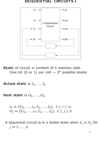
  • 1. SEQUENTIAL CIRCUITS I i1 in o1 om Combinational Circuit I1 Ik O1 Ok State of circuit = content of k memory cells. One bit (0 or 1) per cell → 2k possible states Actual state is I1, . . . , Ik Next state is O1, . . . , Ok oi = f(i1, . . . , in, I1, . . . , Ik), 1 ≤ i ≤ m Oj = f(i1, . . . , in, I1, . . . , Ik), 1 ≤ j ≤ k A sequential circuit is in a stable state when Ij = Oj for j = 1, . . . , k 1
  • 2. Asynchronous Sequential Circuits Responds to a change in one of the inputs Input signals change one at a time and only when the circuit is in a stable state Memory elements = Latches: Two-state circuit that stores one bit SR latch: 2 inputs (S)et, (R)eset, and 2 outputs Q, Q̄ Its equations are: Q = R + p = R̄p̄ P = S + q = S̄q̄ where p, q are the actual states and Q, P are the next states (with P = Q̄) 2
  • 3. Stable States of SR Latch To find the stable states • Obtain truth table of SR latch according to Q = f(q, p, R, S) = R̄p̄ P = f(q, p, R, S) = S̄q̄ • Build a K-map with values of Q,P as entries • Circle entries where Q,P = q,p q p R S Q P 0 0 0 0 1 1 0 0 0 1 1 0 0 0 1 0 0 1 0 0 1 1 0 0 0 1 0 0 0 1 0 1 0 1 0 0 0 1 1 0 0 1 0 1 1 1 0 0 1 0 0 0 1 0 1 0 0 1 1 0 1 0 1 0 0 0 1 0 1 1 0 0 1 1 0 0 0 0 1 1 0 1 0 0 1 1 1 0 0 0 1 1 1 1 0 0 7→ 00 01 11 10 00 11 10 00 01 01 01 00 00 01 11 00 00 00 00 10 10 10 00 00 3
  • 4. Functionality of SR Latch (continued) S,R = 1,1 7→ stable state Q,Q̄ = 0,0 → Q = Q̄ → undefined state. We must avoid inputs S,R = 1,1 simultaneously Q,Q̄ = 0,0 7→ indeterminate next state when S,R becomes 0,0 simultaneously. 00 01 11 10 00 11 10 00 01 01 01 00 00 01 11 00 00 00 00 10 10 10 00 00 S,R = 1,0 7→ set state Q,Q̄ = 1,0 S,R = 0,1 7→ reset state Q,Q̄ = 0,1 S,R = 0,0 7→ next state = actual state of Q,Q̄ 4
  • 5. Functionality of SR Latch (continued) S,R = 0,0 S,R = 0,1 00 01 11 10 00 11 10 00 01 01 01 00 00 01 11 00 00 00 00 10 10 10 00 00 00 01 11 10 00 11 10 00 01 01 01 00 00 01 11 00 00 00 00 10 10 10 00 00 S,R = 1,0 S,R = 1,1 00 01 11 10 00 11 10 00 01 01 01 00 00 01 11 00 00 00 00 10 10 10 00 00 00 01 11 10 00 11 10 00 01 01 01 00 00 01 11 00 00 00 00 10 10 10 00 00 Therefore the truth table of SR latch is 5
  • 6. SR Latch (equivalent representation) S R Q q Its equation is Q = SR̄ + qR̄ Truth table and transition table below q R S Q 0 0 0 0 0 0 1 1 0 1 0 0 0 1 1 0 1 0 0 1 1 0 1 1 1 1 0 0 1 1 1 0 7→ 00 01 11 10 0 0 1 X 0 0 1 1 X 0 ⇒ if SR = 0 (S,R 6= 1,1) then minimal → Q = S + R̄q 6
  • 7. S̄R̄ Latch Uses NAND gates ⇓ When S̄R̄ = 0, that is S,R 6= 0,0 then its equation is Q = S̄ + Rq 7
  • 8. Synchronous Sequential Circuits Responds to a clock pulse State transitions occurs only at fixed time intervals dic- tated by the clock pulses. Time is discrete: the next state can be described at time t + 1 with respect to the actual state at time t More complex design but more reliable than asynchronous circuits. Memory elements = Flip-flops: Two-state circuit that stores one bit 8
  • 9. SR Flip-Flop S C R Q Q’ → Qt S R Qt+1 0 0 0 0 0 0 1 0 0 1 0 1 0 1 1 ? 1 0 0 1 1 0 1 0 1 1 0 1 1 1 1 ? Working conditions: SR = 0. Pulse triggered flip-flop Characteristic equation: (after simplification) Qt+1 = S + R̄Qt Characteristic table S R Qt+1 Operation 0 0 Qt No change 0 1 0 Reset 1 0 1 Set 1 1 ? Undefined Excitation table Qt Qt+1 S R 0 0 0 X 0 1 1 0 1 0 0 1 1 1 X 0 9
  • 10. D Flip-Flop C Q Q’ D → Qt D Qt+1 0 0 0 0 1 1 1 0 0 1 1 1 Working conditions: No undefined state. Edge triggered flip-flop Characteristic equation: (after simplification) Qt+1 = D Characteristic table D Qt+1 Operation 0 0 Reset 1 1 Set Excitation table Qt Qt+1 D 0 0 0 0 1 1 1 0 0 1 1 1 10
  • 11. JK Flip-Flop K C J Q Q’ → Qt J K Qt+1 0 0 0 0 0 0 1 0 0 1 0 1 0 1 1 1 1 0 0 1 1 0 1 0 1 1 0 1 1 1 1 0 Working conditions: No undefined state. Pulse or edge triggered flip-flop Characteristic equation: (after simplification) Qt+1 = JQ̄ + K̄Q Characteristic table J K Qt+1 Operation 0 0 Qt No change 0 1 0 Reset 1 0 1 Set 1 1 Q̄t Complement Excitation table Qt Qt+1 J K 0 0 0 X 0 1 1 X 1 0 X 1 1 1 X 0 11
  • 12. T Flip-Flop Q Q’ C T → Qt T Qt+1 0 0 0 0 1 1 1 0 1 1 1 0 Working conditions: No undefined state. Pulse or edge triggered flip-flop Characteristic equation: (after simplification) Qt+1 = TQ̄ + T̄Q Characteristic table T Qt+1 Operation 0 Qt Reset 1 Q̄t Set Excitation table Qt Qt+1 T 0 0 0 0 1 1 1 0 1 1 1 0 12
  • 13. Standard Graphics Symbols for Latches and Flip-Flops 13
  • 14. Synchronous Sequential Circuit Analysis Given a synchronous sequential circuit, example We can express its behavior in three ways: by 1. Circuit output functions and flip-flops input functions 2. Circuit output functions and state equations 3. State table and state diagram 14
  • 15. Synchronous Sequential Circuit Analysis (Circuit output and flip-flops input functions) Question: What are the values of Y , DA and DB ? Use the information contained in the combinational cir- cuit to obtain the circuit’s outputs and the flip-flops’ inputs. That is • Y = X̄(At + Bt) • DA = X(At + Bt) • DB = XĀt Thus we can represent the states changes and the out- puts. However, this representation is quite useless; we still do not know what the circuit truly does (par- ticularly when we do not know the types of flip-flops used). The following two representations are better. 15
  • 16. Synchronous Sequential Circuit Analysis (Circuit output functions and state equations) Question: Values of Y , At+1 and Bt+1 ? For circuit’s output functions: use the information con- tained in the combinational circuit. That is • Y = X̄(At + Bt) For flip-flops’ state equations: either • Make a truth table and minimize to obtain the state equations. Or, • Substitute the flip-flops’ input functions into the flip-flops’ characteristic equations to obtain the state equations The characteristic equation of D flip-flop is Qt+1 = D, therefore • At+1 = DA = X(At + Bt) • Bt+1 = DB = XĀt 16
  • 17. Synchronous Sequential Circuit Analysis (State table and state diagram) Question: What are the ouputs and next states given the inputs and current states? State table: Enumerates the functional relationships be- tween inputs, outputs, and states flip-flops states of a sequential circuit State diagram: Graphical representation of a state ta- ble For each possible (actual) state of the circuit and for each possible combination of values of input vari- ables: 1. Use the flip-flops’ input functions and their char- acteristic tables to determine the next state of the circuit (A,B in example) 2. Use the circuit’s output functions to determine the output values (Y in example) 17
  • 18. Synchronous Sequential Circuit Analysis (State table and state diagram) (continued) State Table Present state Next state Output X = 0 X = 1 X = 0 X = 1 A B A B A B Y Y 0 0 0 0 0 1 0 0 0 1 0 0 1 1 1 0 1 0 0 0 1 0 1 0 1 1 0 0 1 0 1 0 State Diagram 18
  • 19. Synchronous Sequential Circuit Design 1. Obtain state table from circuit specification (state diagram, state equations or timing diagram) 2. If necessary, assign binary codes to each state of state table 3. Determine the number and type of flip-flops needed and assign a letter to each 4. From the state table, derive the circuit excitation and output tables 5. Using K-maps, derive the circuit output functions and the flip-flops input functions 6. Draw the synchronous sequential logic circuit 19
  • 20. Synchronous Sequential Circuit Design (Example) Given the State diagram or the State equations Y = AtBt + X At+1 = AtB̄t + BtX̄ Bt+1 = AtBtX̄ + Ātx + B̄tX of a synchronous sequential circuit specification Then . . . . . . use the following design method . . . 20
  • 21. Synchronous Sequential Circuit Design (continued) Step 1: Present state Next state Output X = 0 X = 1 X = 0 X = 1 A B A B A B Y Y 0 0 0 0 0 1 0 0 0 1 1 0 0 1 0 1 1 0 1 0 1 1 0 1 1 1 1 1 0 0 1 1 Step 2: Not necessary in our example Step 3: Type of flip-flop is usually given. If not, then select cheapest: in general JK flip-flop Number of flip-flops depends on number of states and the encoding used. In our case we need 2 flip- flops since there are 4 states (2 = log2 4), each coded by two variables. The flip-flops are: JAKA flip-flop and JBKB flip-flop and 21
  • 22. Synchronous Sequential Circuit Design (continued) Step 4: Reorganize the state table in the following way Inputs of CC Inputs of FF Ps Input Ns Output Excitations AB X AB Y JA KA JB KB 00 0 00 0 0 X 0 X 00 1 01 1 0 X 1 X 01 0 10 0 1 X X 1 01 1 01 1 0 X X 0 10 0 10 0 X 0 0 X 10 1 11 1 X 0 1 X 11 0 11 1 X 0 X 0 11 1 00 1 X 1 X 1 ⇑ Excitation table Qt Qt+1 J K 0 0 0 X 0 1 1 X 1 0 X 1 1 1 X 0 Excitation table: what are the values of J and K needed to go from Qt to Qt+1? 22
  • 23. Synchronous Sequential Circuit Design (continued) Step 5: Simplify the by K-maps the circuit’s output Y , and the flip-flops’ inputs JA, KA, JB and KB. After simplification, we obtain: • Y = AB + X • JA = BX̄ • KA = BX • JB = X • KB = ĀX̄ + AX = A ¯ X 23
  • 24. Synchronous Sequential Circuit Design (continued) Step 6: Use the standard graphics symbols for flip-flops Clearly identify the inputs and outputs of the flip-flops, the clock input, as well as the external inputs and outputs of the circuit Try to minimize crossings (difficult problem) Clearly show the intersections 24
  • 25. Synchronous Sequential Circuit Design (continued) Designing With Unused States: If a state is not used (state 11 below), then put an X for the flip-flops’ inputs and the circuit’s output. The final expressions will be much simpler The table below shows only the part of the excitation table (obtained in step 4) that deals with the state 11 Inputs of CC Inputs of FF Ps Input Ns Output Excitations AB X AB Y JA KA JB KB 00 0 00 1 01 0 01 1 10 0 10 1 11 0 XX X X X X X 11 1 XX X X X X X 25