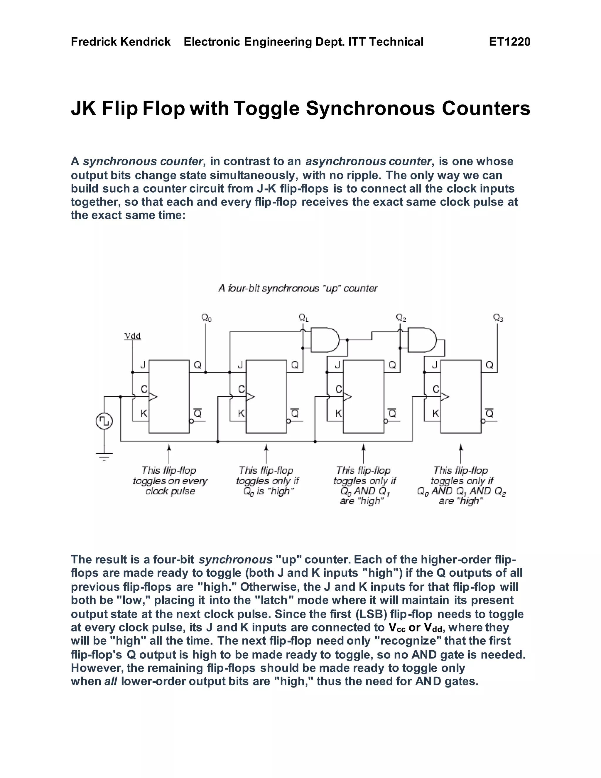
This document discusses the design and operation of a 4-bit synchronous up/down counter using JK flip-flops. It explains that in a synchronous counter, all output bits change state simultaneously in response to a clock signal. The circuit connects all flip-flop clock inputs together. For an up counter, the J and K inputs of each flip-flop are configured to toggle the flip-flop when the outputs of all previous flip-flops are high. For a down counter, the circuit recognizes bit patterns where preceding bits are low before a toggle by using the Q' outputs of each flip-flop. The least significant bit toggles on every clock cycle while more significant bits toggle less frequently in a divide
Flip Flop | Counters & Registers | Computer Fundamental and OrganizationSmit Luvani
Agenda :
Sequential Circuit
R-S/S-R Flip Flop
Active low state
Active High State
Clocked State
J-K Flip Flop
Master Slave Flip Flop
T Flip Flop
D-Flip Flop
Counters :
What is Counter?
Ripple Counter
Synchronous Counter
Binary Ripple Counter
Register
Shift Register
Shift Registers – Serial In Serial Out
Shift Registers – Serial In Parallel Out
Shift Registers – Parallel In Serial Out
Shift Registers – Parallel In Parallel Out
The following presentation is a part of the level 4 module -- Digital Logic and Signal Principles. This resources is a part of the 2009/2010 Engineering (foundation degree, BEng and HN) courses from University of Wales Newport (course codes H101, H691, H620, HH37 and 001H). This resource is a part of the core modules for the full time 1st year undergraduate programme.
The BEng & Foundation Degrees and HNC/D in Engineering are designed to meet the needs of employers by placing the emphasis on the theoretical, practical and vocational aspects of engineering within the workplace and beyond. Engineering is becoming more high profile, and therefore more in demand as a skill set, in today’s high-tech world. This course has been designed to provide you with knowledge, skills and practical experience encountered in everyday engineering environments.
ppt on flip flops
contents :
Made by : Dhanesh RK Nair
WHAT IS FLIP FLOP?
In digital circuits, the flip-flop, is a kind of bistable multivibrator.
It is a Sequential Circuits / an electronic circuit which has two stable states and thereby is capable of serving as one bit of memory , bit 1 or bit 0.
TYPES OF FLIP FLOPS:
1. SR Flip Flop
2. Clocked SR Flip Flop
3. JK Flip Flop
4. JK Flip Flop With Preset And Clear
5. T Flip Flop
6. D Flip Flop
USES OF FLIP FLOPS:
For Memory circuits
For Logic Control Devices
For Counter Devices
For Register Devices
SR FLIP FLOP
The most basic Flip Flop is called SR Flip Flop.
The basic RS flip flop is an asynchronous device.
In asynchronous device, the outputs is immediately changed anytime one or more of the inputs change just as in combinational logic circuits.
It does not operate in step with a clock or timing.
CLOCKED SR FLIP FLOP
Additional clock input is added to change the SR flipflop from an element used in asynchronous sequential circuits to one, which can be used in synchronous circuits.
The clocked SR flip flop logic symbol that is triggered by the PGT
Its means that the flip flop can change the output states only when clock signal makes a transition from LOW to HIGH.
JK FLIP FLOP
Another types of Flip flop is JK flip flop.
It differs from the RS flip flops when J=K=1 condition is not indeterminate but it is defined to give a very useful changeover (toggle) action.
Toggle means that Q and Q(compliment) will switch to their opposite states.
The JK Flip flop has clock input Cp and two control inputs J and K.
Operation of Jk Flip Flop is completely described by truth table
T FLIP FLOP
The T flip flop has only the Toggle and Hold Operation.
If Toggle mode operation. The output will toggle from 1 to 0 or vice versa.
D FLIP FLOP
Also Known as Data Flip flop
Can be constructed from RS Flip Flop or JK Flip flop by addition of an inverter.
Inverter is connected so that the R input is always the inverse of S (or J input is always complementary of K).
The D flip flop will act as a storage element for a single binary digit (Bit).
THANKS....!!!!
SOME MORE CONTENTS :
In electronics, a flip-flop or latch is a circuit that has two stable states and can be used to store state information. A flip-flop is a bistable multivibrator. The circuit can be made to change state by signals applied to one or more control inputs and will have one or two outputs. It is the basic storage element in sequential logic. Flip-flops and latches are fundamental building blocks of digital electronics systems used in computers, communications, and many other types of systems.
Flip-flops and latches are used as data storage elements. A flip-flop stores a single bit (binary digit) of data; one of its two states represents a "one" and the other represents a "zero". Such data storage can be used for storage of state, and such a circuit is described as sequential logic.
THANKS!!!!!!!!!!!
The document explains about the concepts of sequential circuits in Digital electronics.
This will be helpful for the beginners in VLSI and electronics students.
Introduction to Bipolar Junction Transistors (BJTs)Mugisha Oma.docxmariuse18nolet
Introduction to Bipolar Junction Transistors (BJTs)
Mugisha Omary
Introduction to Bipolar Junction Transistors (BJTs)
Laboratory Report for EENG 3306
College of Engineering and Computer Science
Department of Electrical Engineering
University of Texas at Tyler
Houston, TX
December 8, 2014
Mugisha Omary
Group Members
Hamza Ahmad
Shamir Mohammed
I. Project description
The purpose of this lab is to take measurement of the common-emitter characteristics (collector current IC vs collector-to-emitter voltage VCE of small-signal NPN and PNP bipolar transistors and also simulate IC vs VCE characteristics of 2N4401 and 2N3906 transistors.
A BJT is a semiconductor device that uses a small current to control a larger current. This property makes it essentially a current amplifier. In this lab the student will build a simple test circuit to evaluate a transistor’s current and voltage relationships and then use this data to determine the transistors DC value and plot the collector characteristic curve.
II. Theoretical background
A BJT is a three terminal two – junction semiconductor device in which the
conduction is due to both the charge carrier. Hence it is a bipolar device and it
amplifier the sine waveform as they are transferred from input to output. BJT is
classified into two types – NPN or PNP. A NPN transistor consists of two N
types in between which a layer of P is sandwiched. The transistor consists of
three terminal emitter, collector and base. The emitter layer is the source of the
charge carriers and it is heartily doped with a moderate cross sectional area.
The collector collects the charge carries and hence moderate doping and large
cross sectional area. The base region acts a path for the movement of the
charge carriers. In order to reduce the recombination of holes and electrons the
base region is lightly doped and is of hollow cross sectional area. Normally the
transistor operates with the EB junction forward biased. In transistor, the current is same in both junctions, which indicates that there is a transfer of resistance between the two junctions. One to this fact the transistor is known as transfer resistance of transistor.
The symbol of an NPN BJT. The symbol is "not pointing in."
The symbol of a PNP BJT. The symbol "points inproudly."
When a transistor’s base current (IB) is set to a certain value and left unchanged while the collector current is swept through a range of values and IC and VCE are recorded and then graphed, a collector characteristic curve is produced for that particular IB. If IB is now changed, and again the collector current is swept through a range of values, and IC and VCE are plotted, another collector characteristic curve for this different IB value is produced. Repeating this process for several IB values results in a family of curves referred to as the transistors collector characteristic curves. Figure 2 shows the characteristics for a notional transistor.
Figure 1. Transistor.
Latches
– Flip-Flops - SR, JK, D and T
– Master Slave Flip Flops
• Shift Registers
– SISO, SIPO, PISO, PIPO and Universal
• Binary Counters
– Synchronous and asynchronous up/down counters
– mod - N counter
– Counters for random sequence
– Johnson counter and Ring counter
1. Fredrick Kendrick Electronic Engineering Dept. ITT Technical ET1220
JK Flip Flop with Toggle Synchronous Counters
A synchronous counter, in contrast to an asynchronous counter, is one whose
output bits change state simultaneously, with no ripple. The only way we can
build such a counter circuit from J-K flip-flops is to connect all the clock inputs
together, so that each and every flip-flop receives the exact same clock pulse at
the exact same time:
The result is a four-bit synchronous "up" counter. Each of the higher-order flip-
flops are made ready to toggle (both J and K inputs "high") if the Q outputs of all
previous flip-flops are "high." Otherwise, the J and K inputs for that flip-flop will
both be "low," placing it into the "latch" mode where it will maintain its present
output state at the next clock pulse. Since the first (LSB) flip-flop needs to toggle
at every clock pulse, its J and K inputs are connected to Vcc or Vdd, where they
will be "high" all the time. The next flip-flop need only "recognize" that the first
flip-flop's Q output is high to be made ready to toggle, so no AND gate is needed.
However, the remaining flip-flops should be made ready to toggle only
when all lower-order output bits are "high," thus the need for AND gates.
2. Fredrick Kendrick Electronic Engineering Dept. ITT Technical ET1220
To make a synchronous "down" counter, we need to build the circuit to recognize
the appropriate bit patterns predicting each toggle state while counting down. Not
surprisingly, when we examine the four-bit binary count sequence, we see that all
preceding bits are "low" prior to a toggle (following the sequence from bottom to
top):
Since each J-K flip-flop comes equipped with a Q' output as well as a Q output,
we can use the Q' outputs to enable the toggle mode on each succeeding flip-
flop, being that each Q' will be "high" every time that the respective Q is "low:"
Note how the least significant bit (LSB) toggles between 0 and 1 for every step in
the count sequence, while each succeeding bit toggles at one-half the frequency
of the one before it. The most significant bit
(MSB) only toggles once during the entire sixteen-step count sequence: at the
transition between 7 (0111) and 8 (1000).
If we wanted to design a digital circuit to "count" in four-bit binary, all we would
have to do is design a series of frequency divider circuits, each circuit dividing
the frequency of a square-wave pulse by a factor of 2:
3. Fredrick Kendrick Electronic Engineering Dept. ITT Technical ET1220
The NOTES were taken from Don Heller’s Class on 2/13th & 20th/2015. Research
was put into the understanding of this system from your board work. “Thank You
for taking the time to show detail.”