Sequential Circuits
CombinationalCircuits: A circuit whose output, at any instant of time are dependent
upon the input present at that time.
Half Adder, Full Adder
Sequential Circuits: A circuit whose output depends not only on the present inputs
but also on the past history of inputs.
Flipflop
3.
Difference between Combinationaland
Sequential circuits
Combinational Circuits Sequential Circuits
In combinational circuits the output variables at any
instance of time are dependent only on the present
input variables.
In sequential circuits, the output variables at any
instance of time are dependent not only on the
present input variables but also on the present state
i.e. on the past history of the system
Memory unit is not required in combinational circuits Memory unit is required to store the past history of
the input variables in sequential circuits
Combinational circuits are faster because the delay
between the input and the output is due to
propagation delay of gates only.
Sequential circuits are slower than combinational
circuits
Combinational circuits are easy to design Sequential circuits are comparatively harder to design
Examples: Parallel adders, subtractors, encoders,
decoders, code convertors, parity bit generator, etc.
Examples: Counters, shift registers, serial adders,
sequence generators, logic function generators,
memory elements, etc.
4.
Types of SequentialCircuits
Synchronous Sequential Circuit: is a system whose behavior can be defined
from the knowledge of its signals at discrete instant of time.
Asynchronous Sequential Circuit: is a system whose behavior depends upon
the order in which its input signals change and can be affected at any instant
of time.
Clocked Sequential Circuit: Synchronous Sequential Circuits that use clock
pulses in the inputs of memory elements are called Clocked Sequential
Circuit.
5.
Difference between Synchronousand
Asynchronous Sequential circuits
Synchronous Sequential circuits Asynchronous Sequential circuits
In synchronous circuits memory elements are clocked
FFs.
In Asynchronous circuits memory elements are either
unclocked FFs or time delay elements
In Synchronous circuits the change in input signals can
affect memory elements upon activation of clock
signal
In Asynchronous circuits change in input signal can
affect memory elements at any instance of time
The Maximum operating speed of the clock depends
on time delay involved
Because of the absence of the clock asynchronous
circuits can operate faster than synchronous circuits
Easy to design More difficult to design
6.
Latches
Latches aredigital circuits that store a single bit of information and hold its
value until it is updated by new input signals.
They are used in digital systems as temporary storage elements to store
binary information.
Latches can be implemented using various digital logic gates, such as
AND, OR, NOT, NAND, and NOR gates.
7.
Latches
Latches arewidely used in digital systems for various applications,
including data storage, control circuits, and flip-flop circuits.
Used in combination with other digital circuits to implement sequential
circuits, such as state machines and memory elements.
There are two types of latches: S-R (Set-Reset) Latches and D (Data)
Latches, and they are widely used in digital systems for various
applications.
8.
S-R (Set-Reset) Latch
S-R (Set-Reset) Latches: S-R latches are the simplest form of latches and
are implemented using two inputs: S (Set) and R (Reset).
The S input sets the output to 1, while the R input resets the output to 0.
When both S and R are at 1, the latch is said to be in an “undefined” state.
Also known as preset and clear states. The SR latch forms the basic
building blocks of all other types of flip-flops.
SR Latch is a circuit with:
I. 2 cross-coupled NOR gate or 2 cross-coupled NAND gate.
II. 2 input S for SET and R for RESET.
III. 2 output Q, Q’.
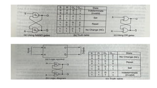
The SR Latchusing NAND gate
Case-1: S’=R’=1 (S=R=0) –
If Q = 1, Q and R’ inputs for 2nd NAND gate are both 1.
If Q = 0, Q and R’ inputs for 2nd NAND gate are 0 and 1 respectively.
12.
The SR Latchusing NAND gate
Case-2: S’=0, R’=1 (S=1, R=0) –
As S’=0, the output of 1st NAND gate, Q = 1(SET state). In 2nd NAND
gate, as Q and R’ inputs are 1, Q’=0.
13.
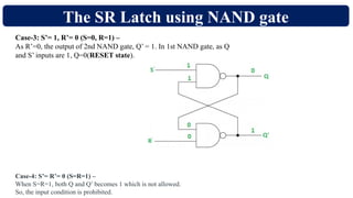
The SR Latchusing NAND gate
Case-3: S’= 1, R’= 0 (S=0, R=1) –
As R’=0, the output of 2nd NAND gate, Q’ = 1. In 1st NAND gate, as Q
and S’ inputs are 1, Q=0(RESET state).
Case-4: S’= R’= 0 (S=R=1) –
When S=R=1, both Q and Q’ becomes 1 which is not allowed.
So, the input condition is prohibited.
14.
The SR Latchusing NAND gate
S R Q
0 0 1 1 Undefined
0 1 1 0 Set
1 0 0 1 Reset
1 1 0 1
Store/
Memory
1 0
16.
The SR Latchusing NOR gate
S R Q
1 1 0 0 Undefined
1 0 1 0 Set
0 1 0 1 Reset
0 0 0 1
Store/
Memory
1 0
17.
Gated SR Latch
A Gated SR latch (clocked SR Latch) is a SR latch with enable input which
works when enable is 1 and retain the previous state when enable is 0.
18.
D (Data) Latch
D latches are also known as transparent latches and are implemented using two inputs: D (Data)
and a clock signal.
The output of the latch follows the input at the D terminal as long as the clock signal is high.
When the clock signal goes low, the output of the latch is stored and held until the next rising
edge of the clock.
19.
Gated D (Data)Latch
The Gated D Latch is another special type of gated latch having two inputs, i.e., DATA and
ENABLE. When the enable input set to 1, the input is the same as the Data input. Otherwise,
there is no change in output.
Enable D Q(n) Q(n+1) STATE
1 0 x 0 RESET
1 1 x 1 SET
0 x x Q(n)
No
Change
20.
Advantages of Latches
Easy to Implement: Latches are simple digital circuits that can be easily implemented
using basic digital logic gates.
Low Power Consumption: Latches consume less power compared to other sequential
circuits such as flip-flops.
High Speed: Latches can operate at high speeds, making them suitable for use in high-
speed digital systems.
Low Cost: Latches are inexpensive to manufacture and can be used in low-cost digital
systems.
Versatility: Latches can be used for various applications, such as data storage, control
circuits, and flip-flop circuits.
21.
Disadvantages of Latches
No Clock: Latches do not have a clock signal to synchronize their operations, making their
behavior unpredictable.
Unstable State: Latches can sometimes enter into an unstable state when both inputs are at
1. This can result in unexpected behavior in the digital system.
Complex Timing: The timing of latches can be complex and difficult to specify, making
them less suitable for real-time control applications.
22.
Flip Flop
Acircuit that has two stable states is treated as a flip flop.
These stable states are used to store binary data that can be changed by applying varying
inputs.
The flip flops are the fundamental building blocks of the digital system.
Flip flops and latches are examples of data storage elements.
In the sequential logical circuit, the flip flop is the basic storage element.
The latches and flip flops are the basic storage elements but different in working.
SR Flip Flop
SRflip-flop operates with only positive clock transitions or negative clock transitions.
Whereas, SR latch operates with enable signal.
Characteristics Equation for SR Flip Flop: QN+1 = QNR’ + S
25.
D Flip-Flop
D flip-flopoperates with only positive clock transitions or negative clock transitions.
Whereas, D latch operates with enable signal. That means, the output of D flip-flop is
insensitive to the changes in the input, D except for active transition of the clock signal.
Characteristics Equation for D Flip Flop: Qt+1 = D
D flip-flop is always equal to data input, D for every positive transition of the clock
signal. Hence, D flip-flops can be used in registers, shift registers and some of the
counters.
26.
JK Flip-Flop
JK flip-flopis the modified version of SR flip-flop. It operates with only positive clock
transitions or negative clock transitions.
Characteristics Equation for JK Flip Flop: QN+1 = JQN’ + K’ QN
27.
T Flip-Flop
T flip-flopis the simplified version of JK flip-flop. It is obtained by connecting the same
input ‘T’ to both inputs of JK flip-flop. It operates with only positive clock transitions or
negative clock transitions.
Characteristics Equation for JK Flip Flop: QN+1 = TQN’ + T’ QN = T ⊕ QN
Similarly, we can implement these flip-flops by using NOR gates.
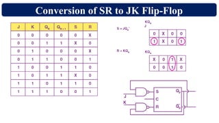
Converting Flip-Flops
The stepsthat one must use to convert one given flip-flop to another one. Let us assume
that we have the required flip-flops that are to be constructed using the sub-flip-flops:
1. Drawing of the truth of the required flip-flop.
2. Writing of the corresponding outputs of those sub-flip-flops that are to be used from
the given excitation table.
3. Drawing of the K-Maps using the required inputs of the flip-flops and then obtaining
the excitation functions for the inputs of the sub-flip-flops.
4. Construction of the logic diagram in accordance with the functions that we have
obtained.
Applications of Flip-Flops
Parallel data storage
Serial data storage
Transfer of data
Serial to parallel conversion
Parallel to serial conversion
Frequency dividers
Counters
What is anEdge-Triggered Flip-Flop?
The type of digital circuit which is capable of storing 1-bit of information and responds
only when a specific edge of the clock pulse occurs is known as an edge-triggered flip-
flop.
The output state of the edge-triggered flip flop updates only when a specific edge of the
clock pulse occurs, i.e. the clock pulse goes from either low to high or high to low states.
This flip flop does not respond to a continuous clock pulse.
Edge-triggered flip-flop are used in several digital circuits where the output of the flip flop
should be updated when the clock pulse changes its state from 0 to 1 or 1 to 0
0
1 1
0
Rising
edge
Falling
edge
High
Low
38.
Positive Edge-Triggered Flip-Flop
The type of edge-triggered flip-flop whose output changes its state only on the rising edge
(edge that goes from low to high) of the clock pulse is called a positive edge-triggered flip-
flop.
The positive edge triggered flip flop is also called a rising edge-triggered flip-flop.
D Q
Q’
˃ CLK
In a positive edge triggered flip flop, the inputs are accepted and stored only when the
clock pulse goes from low (0) to high (1), i.e. on the rising edge of the clock pulse.
This stored value is then available on the outputs
39.
Negative Edge-Triggered Flip-Flop
The type of edge-triggered flip flop whose output changes its state only on the falling edge
(edge that goes from high to low) of the clock pulse is called a negative edge-triggered
flip-flop.
The negative edge triggered flip flop is also known as a falling edge-triggered flip-flop.
D Q
Q’
˃ CLK
In the case of negative edge triggered flip flop, the flip-flop captures and stores the inputs
only when the clock pulse goes from high to low, i.e. on falling edge of the clock pulse.
40.
Edge-Triggered D Flip-Flop
•CP = 0 => S & R = 1 => STEADY
STATE OUTPUT
• D = 0 & CP = 1 => S = 1, R = 0 => Q = 0
• D = 1 & CP = 1 => S = 0, R = 1 => Q = 1
41.
Edge-Triggered JK Flip-Flop
In figure logic diagram of a positive edge
triggered JK flip-flop along with its timing
diagram has been denoted.
Two data inputs J and K are also visible besides
clock input.
A short time constant circuit along CLK input has
been demonstrated, which converts quadrate-type
clock pulse into narrow spikes, as has been
depicted in the diagram.
It is obvious from the logic diagram that Q output
has been connected or feedback with bottom
NAND gate whereas Q output connected with top
NAND gate (that’s JK flip-flop is a double
feedback circuit).
This circuit is a positive edged-triggered circuit
owing to a double inversion via NAND gates. In
other words, inputs are enabled (or operate) only
on the rising edge of the clock.
42.
Edge-Triggered SR Flip-Flop
To adjust the clocked RS latch for edge triggering, we must actually combine two identical clocked latch
circuits, but have them operate on opposite halves of the clock signal.
The edge-triggered SR NAND flip-flop is shown below.
43.
Advantages of Edge-TriggeredFlip-Flop
Edge triggered flip flops have an improved timing behavior as compared to the level
triggered flip flops. This is because, the edge triggered flip flop responds only on the
transition of clock pulse.
It reduces the possibility of glitches that cause errors in the system.
It consumes relative low power than the level-triggered flip flops.
It has relatively less complex circuit design.
It can be easily integrated in the form of digital ICs.
Useful in digital systems having very high clock speed.
44.
Master-Slave JK FlipFlop
For J-K flip-flop, if J=K=1, and if CLK=1 for a long period of time, then Q output will
toggle as long as CLK is high, which makes the output of the flip-flop unstable or
uncertain.
This problem is called race around condition in J-K flip-flop.
This problem can be avoided by ensuring that the clock input is at logic “1” only for a
very short time.
This introduced the concept of Master Slave JK flip flop.
45.
Master-Slave JK FlipFlop
Master Slave JK flip flop – The Master-Slave Flip-Flop is basically a combination of
two JK flip-flops connected together in a series configuration. Out of these, one acts as
the “master” and the other as a “slave”.
The output from the master flip flop is connected to the two inputs of the slave flip
flop whose output is fed back to inputs of the master flip flop. In addition to these two
flip-flops, the circuit also includes an inverter.
The inverter is connected to clock pulse in such a way that the inverted clock pulse is
given to the slave flip-flop. In other words if CP=0 for a master flip-flop, then CP=1
for a slave flip-flop and if CP=1 for master flip flop then it becomes 0 for slave flip
flop.
Master-Slave JK FlipFlop
1. When the clock pulse goes to 1, the slave is isolated; J and K inputs may affect the
state of the system. The slave flip-flop is isolated until the CP goes to 0. When the CP
goes back to 0, information is passed from the master flip-flop to the slave and output
is obtained.
2. Firstly the master flip flop is positive level triggered and the slave flip flop is negative
level triggered, so the master responds before the slave.
3. If J=0 and K=1, the high Q’ output of the master goes to the K input of the slave and
the clock forces the slave to reset, thus the slave copies the master.
4. If J=1 and K=0, the high Q output of the master goes to the J input of the slave and the
Negative transition of the clock sets the slave, copying the master.
5. If J=1 and K=1, it toggles on the positive transition of the clock and thus the slave
toggles on the negative transition of the clock.
6. If J=0 and K=0, the flip flop is disabled and Q remains unchanged.
Master-Slave JK FlipFlop
1. When the Clock pulse is high the output of master is high and remains high till the
clock is low because the state is stored.
2. Now the output of master becomes low when the clock pulse becomes high again and
remains low until the clock becomes high again.
3. Thus toggling takes place for a clock cycle.
4. When the clock pulse is high, the master is operational but not the slave thus the
output of the slave remains low till the clock remains high.
5. When the clock is low, the slave becomes operational and remains high until the clock
again becomes low.
6. Toggling takes place during the whole process since the output is changing once in a
cycle.
Advantages of Master-SlaveFlip Flop
We can operate master-slave flip flops on level-triggered or edge-triggered clock pulse.
We can use it in various ways.
A sequential circuit with a level-triggered flip flop is challenging to design, but edge
triggered flip flop is easy to design.
Most importantly, we can eliminate the Race around condition using the master-slave
flip flop configuration.


![Unit 2[1] . technology with the informationpptx](https://cdn.slidesharecdn.com/ss_thumbnails/unit21-250302040241-815cd69e-thumbnail.jpg?width=640&height=640&fit=bounds)


